 | –≠–ª–µ–∫—Ç—Ä–æ–Ω–Ω—ã–π –∫–æ–º–ø–æ–Ω–µ–Ω—Ç: SC4518 | –°–∫–∞—á–∞—Ç—å:  PDF PDF  ZIP ZIP |
POWER MANAGEMENT
1
www.semtech.com
SC4518
600kHz, 1.5A Step-Down
Switching Regulator
Description
Features
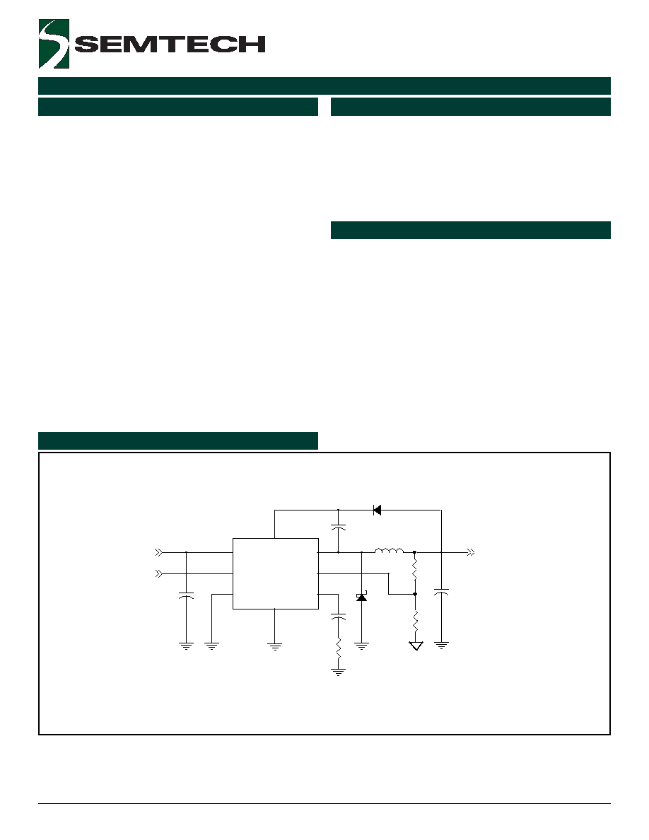
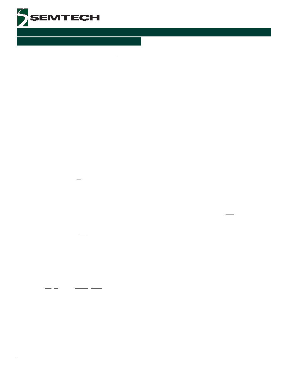
Typical Application Circuit
Applications
Revision: October 6, 2004
The SC4518 is a current mode switching regulator with
an integrated switch, operating at 600kHz with separate
sync & enable functions. The integrated switch allows
for cost effective low power solutions (peak switch current
1.5 amps). The sync function allows customers to
synchronize to a faster clock in order to avoid frequency
beating in noise sensitive applications. High frequency
of operation allows for very small passive components.
Current mode operation allows for fast dynamic response
& instantaneous duty cycle adjustment as the input varies
(ideal for CPE applications where the input is a wall plug
power).
The low shutdown current makes it ideal for portable
applications where battery life is important.
The SC4518 is a 600kHz switching regulator
synchronizable to a faster frequency from 750kHz to
1.2MHz.
Integrated 1.5 Amp switch
600kHz frequency of operation
Current mode controller
Synchronizable to higher frequency up to 1.2MHz
6µA low shutdown current
SO-8 EDP package
XDSL modems
CPE equipment
DC-DC point of load applications
Portable equipment
C1
VOUT
D2
D1
R3
C2
L1
Enable
BST
1
IN
2
SW
3
GND
4
EN
5
FB
6
COMP
7
SYNC
8
VIN
C4
C3
SC4518
R1
R2
2
2004 Semtech Corp.
www.semtech.com
POWER MANAGEMENT
SC4518
r
e
t
e
m
a
r
a
P
l
o
b
m
y
S
s
t
i
m
i
L
s
t
i
n
U
e
g
a
tl
o
V
y
l
p
p
u
S
t
u
p
n
I
V
N
I
6
1
+
o
t
3
.
0
-
V
V
e
v
o
b
A
n
i
P
t
s
o
o
B
W
S
V
(
T
S
B
V
-
W
S
)
6
1
V
e
g
a
tl
o
V
n
i
P
t
s
o
o
B
V
T
S
B
2
3
+
o
t
3
.
0
-
V
e
g
a
tl
o
V
n
i
P
N
E
V
N
E
6
1
+
o
t
3
.
0
-
V
e
g
a
tl
o
V
n
i
P
B
F
V
B
F
6
+
o
t
3
.
0
-
V
t
n
e
r
r
u
C
n
i
P
B
F
I
B
F
1
A
m
t
n
e
r
r
u
C
n
i
P
C
N
Y
S
I
C
N
Y
S
1
A
m
t
n
e
i
b
m
A
o
t
n
o
it
c
n
u
J
e
c
n
a
d
e
p
m
I
l
a
m
r
e
h
T
)
1
(
A
J
5
.
6
3
W
/
C
∞
e
g
n
a
R
e
r
u
t
a
r
e
p
m
e
T
t
n
e
i
b
m
A
g
n
it
a
r
e
p
O
T
A
5
8
+
o
t
0
4
-
C
∞
g
n
it
a
r
e
p
O
e
g
n
a
R
e
r
u
t
a
r
e
p
m
e
T
n
o
it
c
n
u
J
T
J
0
5
1
+
o
t
0
4
-
C
∞
e
g
n
a
R
e
r
u
t
a
r
e
p
m
e
T
e
g
a
r
o
t
S
T
G
T
S
0
5
1
+
o
t
5
6
-
C
∞
c
e
s
0
1
)
g
n
ir
e
d
l
o
S
(
e
r
u
t
a
r
e
p
m
e
T
d
a
e
L
T
D
A
E
L
0
0
3
C
∞
)l
e
d
o
M
y
d
o
B
n
a
m
u
H
(
g
n
it
a
R
D
S
E
D
S
E
2
V
k
r
e
t
e
m
a
r
a
P
l
o
b
m
y
S
s
n
o
i
t
i
d
n
o
C
n
i
M
p
y
T
x
a
M
s
t
i
n
U
ti
m
i
L
t
n
e
r
r
u
C
h
c
ti
w
S
m
u
m
i
x
a
M
I
W
S
0
.
2
A
y
c
n
e
u
q
e
r
F
r
o
t
a
ll
i
c
s
O
f
C
S
O
0
5
5
5
2
6
0
5
7
z
H
k
p
o
r
D
e
g
a
tl
o
V
n
O
h
c
ti
w
S
V
)
W
S
(
D
I
W
S
A
5
.
1
=
0
3
3
V
m
V
N
I
t
u
o
k
c
o
L
e
g
a
tl
o
v
r
e
d
n
U
V
O
L
V
U
0
6
.
2
3
V
V
N
I
t
n
e
r
r
u
C
y
l
p
p
u
S
I
Q
V
B
F
V
=
)
M
O
N
(
T
U
O
%
7
1
+
0
.
1
5
A
m
t
n
e
r
r
u
C
y
b
d
n
a
t
S
I
)
F
F
O
(
Q
V
N
E
V
,
V
0
=
N
I
V
,
V
6
1
=
W
S
V
0
=
5
5
4
A
µ
Electrical Characteristics
Note: (1) Minimum pad size.
Unless specified: V
IN
= 12V, V
COMP
= 0.8V, V
BST
= V
IN
+ 5V, EN = tied to V
IN
, SYNC = 0, SW = open.
T
A
= T
J
= -40∞C to 125∞C.
Absolute Maximum Ratings
Exceeding the specifications below may result in permanent damage to the device, or device malfunction. Operation outside of the parameters
specified in the Electrical Characteristics section is not implied.
3
2004 Semtech Corp.
www.semtech.com
POWER MANAGEMENT
SC4518
R
E
T
E
M
A
R
A
P
L
O
B
M
Y
S
S
N
O
I
T
I
D
N
O
C
N
I
M
P
Y
T
X
A
M
S
T
I
N
U
t
n
e
r
r
u
C
t
u
p
n
I
B
F
I
B
F
5
2
.
0
-
0
5
.
0
-
A
µ
e
g
a
tl
o
V
k
c
a
b
d
e
e
F
V
<
V
3
N
I
V
6
1
<
)
1
(
6
7
1
.
1
2
.
1
4
2
2
.
1
V
e
n
i
L
e
g
a
tl
o
V
k
c
a
b
d
e
e
F
n
o
it
a
l
u
g
e
R
3
+
V
/
V
m
V
o
t
B
F
P
M
O
C
n
i
a
G
e
g
a
tl
o
V
)
2
(
V
4
.
0
V
P
M
O
C
V
9
.
0
0
5
1
0
5
3
V
o
t
B
F
P
M
O
C
e
c
n
a
t
c
u
d
n
o
c
s
n
a
r
T
)
2
(
I
P
M
O
C
=
±
A
µ
0
1
0
0
5
0
5
8
0
0
3
1
o
h
M
µ
V
P
M
O
C
t
n
e
r
r
u
C
e
c
r
u
o
S
n
i
P
V
B
F
V
=
)
M
O
N
(
T
U
O
%
7
1
-
0
7
0
0
1
A
µ
V
P
M
O
C
t
n
e
r
r
u
C
k
n
i
S
n
i
P
V
B
F
V
=
)
M
O
N
(
T
U
O
%
7
1
+
0
7
0
0
1
A
µ
V
P
M
O
C
t
n
e
r
r
u
C
h
c
ti
w
S
o
t
n
i
P
e
c
n
a
t
c
u
d
n
o
c
s
n
a
r
T
5
.
2
V
/
A
V
P
M
O
C
m
u
m
i
x
a
M
n
i
P
d
l
o
h
s
e
r
h
T
g
n
i
h
c
ti
w
S
%
0
=
e
l
c
y
c
y
t
u
D
5
3
.
0
V
V
P
M
O
C
d
l
o
h
s
e
r
h
T
n
i
P
I
W
S
A
5
.
1
=
9
.
0
V
e
l
c
y
C
y
t
u
D
h
c
ti
w
S
m
u
m
i
x
a
M
V
P
M
O
C
I
,
V
2
.
1
=
W
S
A
m
0
0
4
=
5
8
5
9
%
e
g
a
tl
o
V
t
s
o
o
B
m
u
m
i
n
i
M
h
c
ti
w
S
e
v
o
b
A
I
W
S
C
∞
0
,
A
5
.
1
=
T
A
d
n
a
C
∞
5
2
1
I
W
S
T
,
A
3
.
1
=
A
C
∞
0
<
8
.
1
7
.
2
V
t
n
e
r
r
u
C
t
s
o
o
B
I
W
S
A
5
.
0
=
0
1
5
1
A
m
I
W
S
C
∞
0
,
A
5
.
1
=
T
A
d
n
a
C
∞
5
2
1
I
W
S
T
,
A
3
.
1
=
A
C
∞
0
<
0
3
5
4
Electrical Characteristics
(Cont.)
Unless specified: V
IN
= 12V, V
COMP
= 0.8V, V
BST
= V
IN
+ 5V, EN = tied to V
IN
, SYNC = 0, SW = open.
T
A
= T
J
= -40∞C to 125∞C.
4
2004 Semtech Corp.
www.semtech.com
POWER MANAGEMENT
SC4518
Marking Information
Electrical Characteristics
(Cont.)
R
E
T
E
M
A
R
A
P
L
O
B
M
Y
S
S
N
O
I
T
I
D
N
O
C
N
I
M
P
Y
T
X
A
M
S
T
I
N
U
e
g
a
tl
o
V
d
l
o
h
s
e
r
h
T
t
u
p
n
I
e
l
b
a
n
E
V
H
I
2
V
V
L
I
4
.
0
V
t
n
e
r
r
u
C
s
a
i
B
t
u
p
n
I
e
l
b
a
n
E
I
L
I
d
l
o
h
s
e
r
h
t
e
v
o
b
a
V
m
0
6
=
N
E
5
.
2
A
µ
I
H
I
d
l
o
h
s
e
r
h
t
w
o
l
e
b
V
m
0
0
1
=
N
E
5
5
1
A
µ
e
g
a
tl
o
V
d
l
o
h
s
e
r
h
T
C
N
Y
S
5
.
1
V
y
c
n
e
u
q
e
r
F
t
u
p
n
I
C
N
Y
S
)
3
(
0
0
7
0
0
2
1
z
H
k
e
c
n
a
t
s
i
s
e
R
n
i
P
C
N
Y
S
V
C
N
Y
S
V
5
.
0
=
0
2
k
Notes:
(1) The required minimum input voltage for a regulated output depends on the output voltage and load condition.
(2) Guaranteed by design.
(3) For SYNC applications, please contact factory.
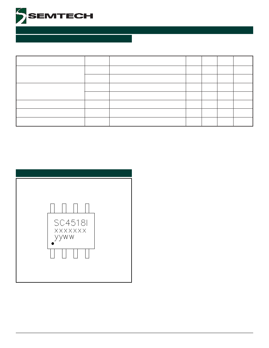
SC4518IES
TOP VIEW
yyww = Date Code (Example: 0012)
xxxx = Semtech Lot No. (Example: E901
xxxx 01-1)
Unless specified: V
IN
= 12V, V
COMP
= 0.8V, V
BST
= V
IN
+ 5V, EN = tied to V
IN
, SYNC = 0, SW = open.
T
A
= T
J
= -40∞C to 125∞C.
5
2004 Semtech Corp.
www.semtech.com
POWER MANAGEMENT
SC4518
Pin Configurations
Ordering Information
r
e
b
m
u
N
t
r
a
P
)
2
(
)
1
(
e
g
a
k
c
a
P
T
R
T
S
I
8
1
5
4
C
S
P
D
E
8
-
O
S
Notes:
(1) Only available in tape and reel packaging. A reel
contains 2500 devices.
(2) Lead free product. This product is fully WEEE and
RoHS compliant.
#
n
i
P
e
m
a
N
n
i
P
n
o
i
t
c
n
u
F
n
i
P
1
T
S
B
h
c
ti
w
s
s
i
h
t
r
o
f
e
g
a
tl
o
v
n
o
n
r
u
t
m
u
m
i
n
i
m
e
h
T
.
h
c
ti
w
s
N
P
N
l
a
n
r
e
t
n
i
e
h
t
o
t
r
e
w
o
p
s
e
d
i
v
o
r
p
n
i
p
s
i
h
T
.
V
7
.
2
s
i
2
N
I
g
n
ir
u
d
t
d
/i
d
h
g
i
h
s
e
e
s
n
i
p
s
i
h
T
.
y
r
ti
u
c
r
i
c
r
e
w
o
p
d
n
a
l
o
r
t
n
o
c
y
b
d
e
r
i
u
q
e
r
r
e
w
o
p
ll
a
s
r
e
v
il
e
d
N
I
n
i
P
s
a
e
s
o
l
c
s
a
n
i
p
s
i
h
t
o
t
d
e
h
c
a
tt
a
e
b
d
l
u
o
h
s
r
o
ti
c
a
p
a
c
g
n
il
p
u
o
c
e
d
A
.
h
c
ti
w
s
e
h
t
f
o
s
n
o
it
c
a
g
n
i
h
c
ti
w
s
.
e
l
b
i
s
s
o
p
3
W
S
d
e
t
c
e
n
n
o
c
e
b
d
l
u
o
h
s
e
d
o
i
d
g
n
il
e
e
h
w
e
e
r
f
l
a
n
r
e
t
x
e
e
h
T
.
h
c
ti
w
s
l
a
n
r
e
t
n
i
e
h
t
f
o
r
e
tt
i
m
e
e
h
t
s
i
W
S
n
i
P
.
n
i
p
s
i
h
t
o
t
e
l
b
i
s
s
o
p
s
a
e
s
o
l
c
s
a
4
D
N
G
g
n
il
e
e
h
w
e
e
r
f
e
h
t
d
n
a
r
o
ti
c
a
p
a
c
g
n
il
p
u
o
c
e
d
e
h
T
.
n
i
p
s
i
h
t
o
t
t
c
e
p
s
e
r
h
ti
w
d
e
r
u
s
a
e
m
e
r
a
s
e
g
a
tl
o
v
ll
A
.
e
l
b
i
s
s
o
p
s
a
t
r
o
h
s
s
a
D
N
G
o
t
d
e
t
c
e
n
n
o
c
e
b
d
l
u
o
h
s
e
d
o
i
d
5
N
E
.
w
o
l
s
i
N
E
fi
ff
o
s
i
ti
d
n
a
,
h
g
i
h
s
i
N
E
fi
n
o
d
e
h
c
ti
w
s
s
i
r
o
t
a
l
u
g
e
r
e
h
T
.t
u
p
n
i
e
l
b
a
n
e
p
i
h
c
e
h
t
s
i
s
i
h
T
w
e
f
a
o
t
d
e
c
u
d
e
r
s
i
t
n
e
r
r
u
c
y
l
p
p
u
s
t
u
p
n
i
e
h
t
d
n
a
,
w
o
l
s
i
N
E
n
e
h
w
e
d
o
m
y
b
d
n
a
t
s
n
i
s
i
r
o
t
a
l
u
g
e
r
e
h
T
.
s
e
r
e
p
m
a
o
r
c
i
m
6
B
F
.
s
r
e
ll
o
r
t
n
o
c
t
u
p
t
u
o
e
l
b
a
t
s
u
j
d
a
r
o
f
t
u
p
n
i
k
c
a
b
d
e
e
F
7
P
M
O
C
A
.r
o
t
a
r
a
p
m
o
c
t
n
e
r
r
u
c
k
a
e
p
e
h
t
f
o
t
u
p
n
i
d
n
a
r
e
if
il
p
m
a
r
o
r
r
e
l
a
n
r
e
t
n
i
e
h
t
f
o
t
u
p
t
u
o
e
h
t
s
i
s
i
h
T
.
e
c
n
a
m
r
o
f
r
e
p
d
e
if
i
c
e
p
s
e
h
t
e
v
e
i
h
c
a
o
t
n
i
p
s
i
h
t
o
t
d
e
t
c
e
n
n
o
c
s
i
k
r
o
w
t
e
n
n
o
it
a
s
n
e
p
m
o
c
8
C
N
Y
S
e
s
l
u
p
l
a
n
r
e
t
x
e
n
a
o
t
r
o
t
a
ll
i
c
s
o
l
a
n
r
e
t
n
i
e
h
t
e
z
i
n
o
r
h
c
n
y
s
o
t
d
e
s
u
n
i
p
l
o
r
t
n
o
c
s
u
o
n
o
r
h
c
n
y
s
s
i
s
i
h
T
.
D
N
G
o
t
d
e
t
c
e
n
n
o
c
e
b
d
l
u
o
h
s
ti
,
d
e
s
u
t
o
n
n
e
h
W
.l
a
n
g
i
s
l
o
r
t
n
o
c
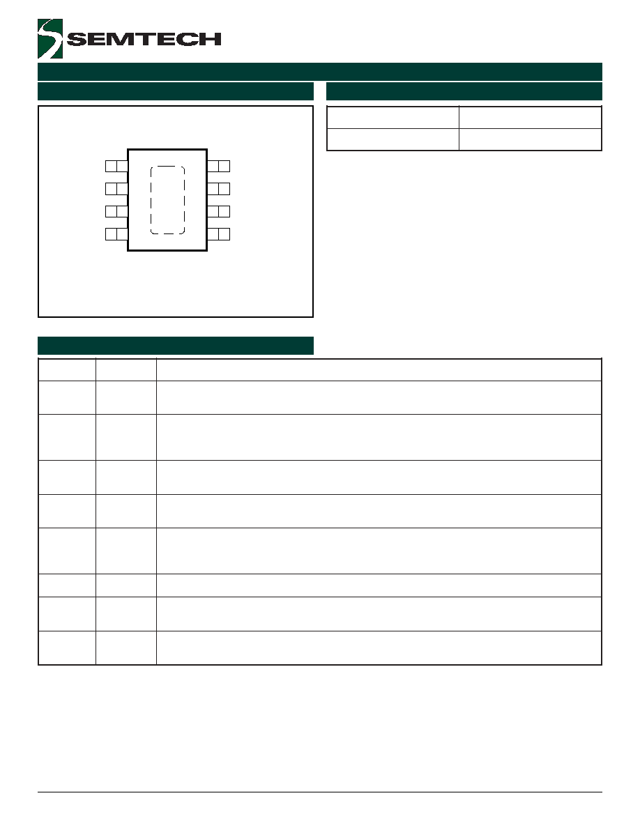
Pin Descriptions
1
2
3
4
SYNC
BST
TOP VIEW
(SO-8 EDP)
5
6
7
8
COMP
IN
FB
SW
EN
GND
6
2004 Semtech Corp.
www.semtech.com
POWER MANAGEMENT
SC4518
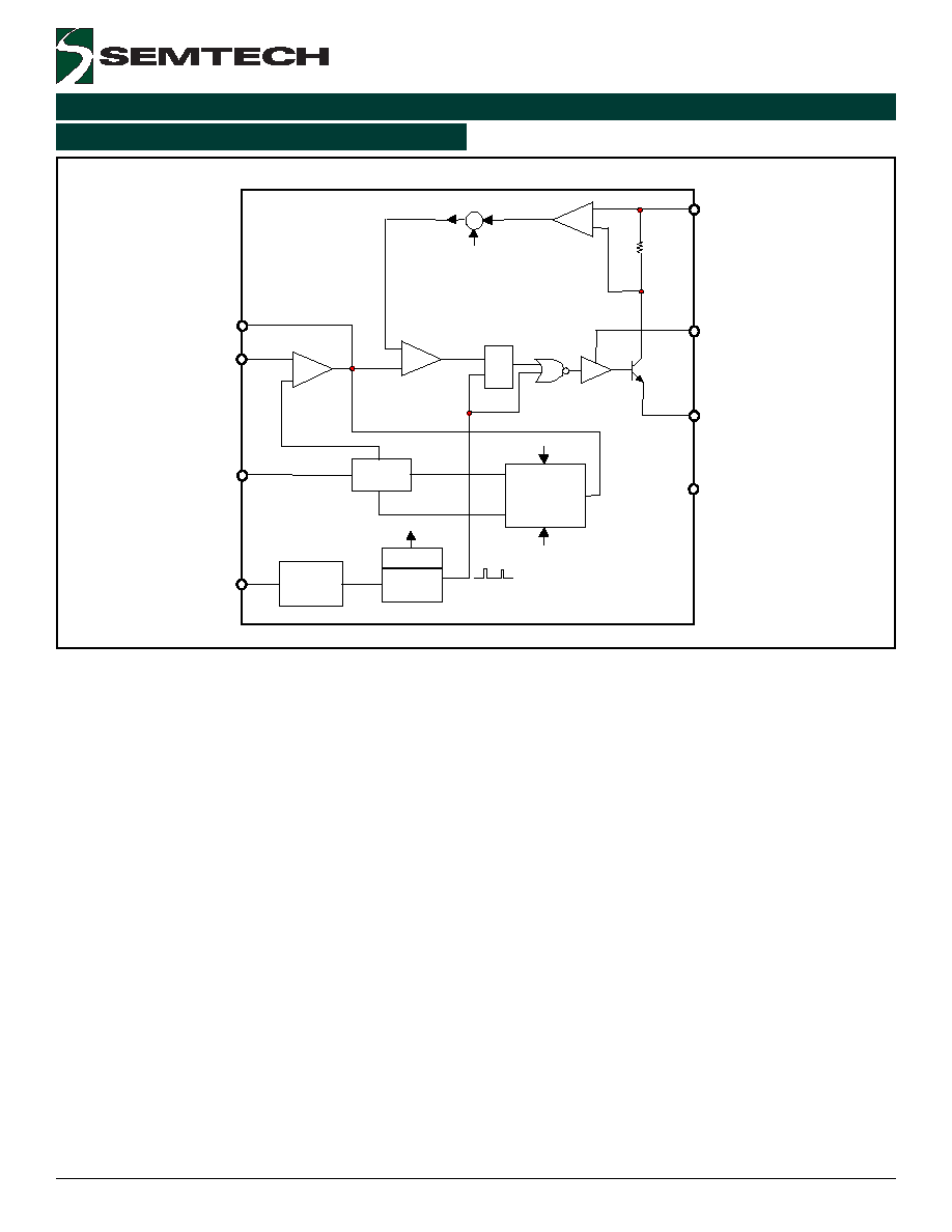
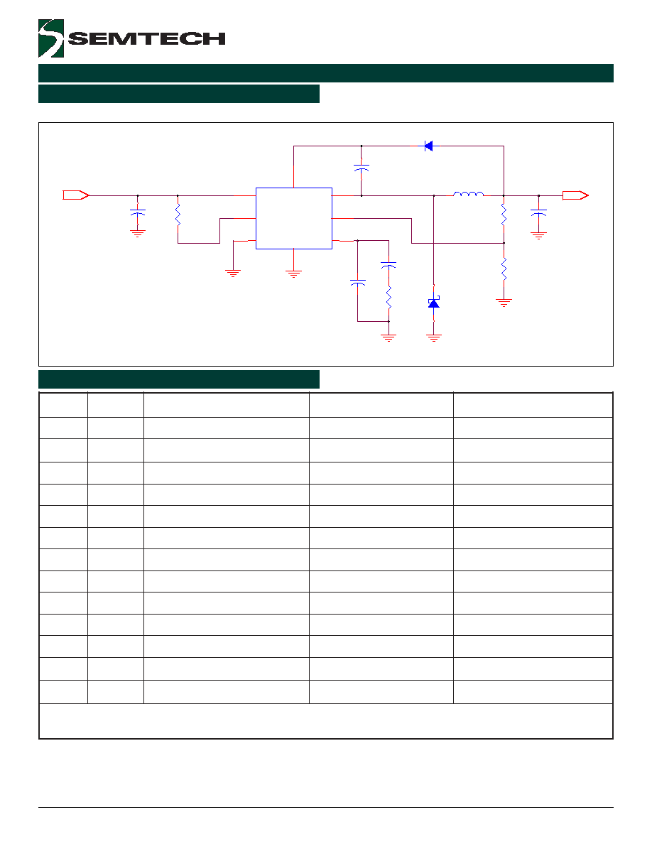
Block Diagram
FB
COMP
R
Q
S
PWM
-
+
POWER
IN
TRANSISTOR
SLOPE
+
+
+
ISEN
40m
SW
BST
OSCILLATOR
CLK
FREQUENCY
SLOPE COMP
SYNC
SLOPE
OL
FB
EN
REFERENCE
1V
UVLO
0.7V
EA
SOFT START
HICCUP
Is
Is
GND
FB
COMP
R
Q
S
PWM
-
+
POWER
IN
TRANSISTOR
SLOPE
+
+
+
ISEN
40m
SW
BST
OSCILLATOR
CLK
FREQUENCY
SLOPE COMP
SYNC
SLOPE
OL
FB
EN
REFERENCE
1V
UVLO
0.7V
EA
SOFT START
HICCUP
Is
Is
GND
7
2004 Semtech Corp.
www.semtech.com
POWER MANAGEMENT
SC4518
Application Information
General Overview
The SC4518 is a current mode buck converter regulator.
SC4518 has an internal fixed-frequency clock. The
SC4518 uses two feedback loops that control the duty
cycle of the internal power switch. The error amplifier
functions like the one of the voltage mode converter.
The current sense amplifier in the SC4518 monitors the
switch current during each cycle. If the output voltage is
lower than 68.75% of its nominal value along with an
over-current condition, a hiccup mode operation is
invoked to prevent excess power dissipation in the switch.
Setting the RS flip-flop from an oscillator pulse turns on
the switch. As the switch peak current reaches a level
preset by the inverting input of the comparator, the flip-
flop is reset and then the switch is turned off. The output
of the error amplifier works as a switch current reference.
This technique effectively removes one of the double
poles in the voltage mode system. With this, it is much
easier to compensate a current mode converter to have
better performance. A minimum 2.7V voltage is required
to saturate the switch when it is on to reduce its
conduction loss.
Enable
Pulling and holding the EN pin below 0.4V activates the
shut down mode of the SC4518 which reduces the input
supply current to less than 10
µ
A. During the shut down
mode, the switch is turned off. The SC4518 is turned on
if the EN pin is pulled high.
Oscillator
Its internal free running oscillator sets the PWM frequency
at 600kHz for the SC4518 without any external
components to program the frequency. An external clock
with a duty cycle from 20% to 80% connected to the
SYNC pin activates synchronous mode. The frequency
of the external clock can be from 750kHz to 1.2MHz.
UVLO
When the EN pin is pulled and held above 1.8V, the voltage
on Pin IN determines the operation of the SC4518. As
VIN increases during power up, the internal circuit senses
VIN and keeps the power transistor off until VIN reaches
2.6V.
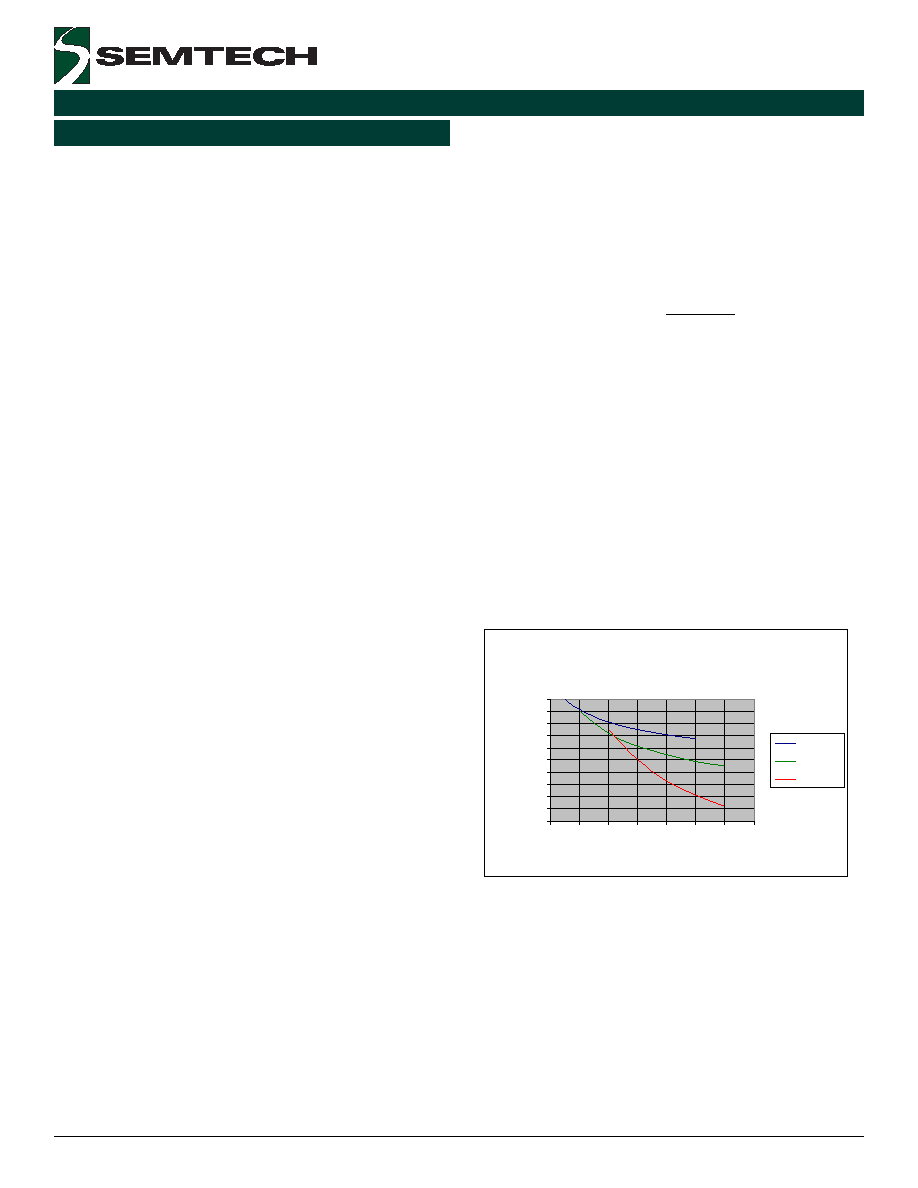
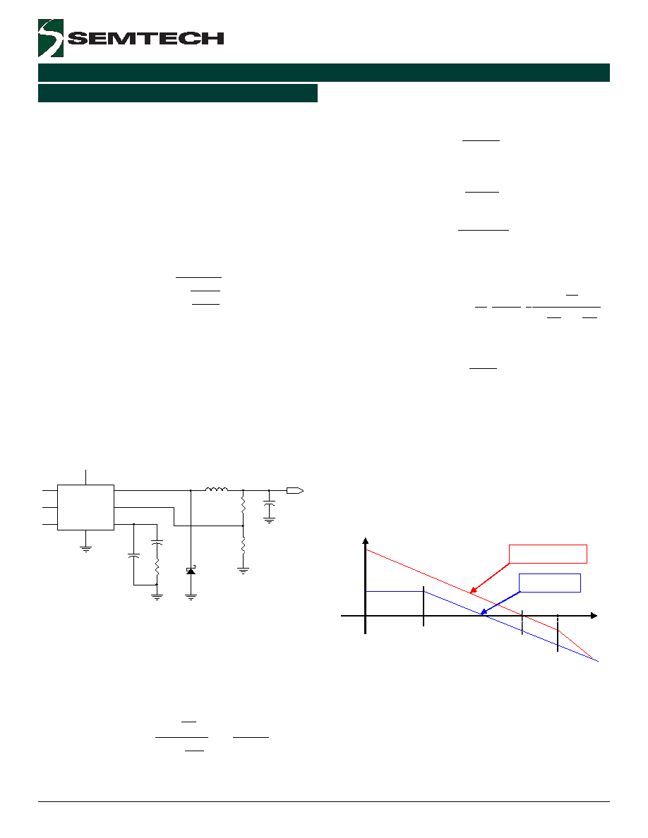
Load Current
The peak current I
PEAK
in the switch is internally limited.
For a specific application, the allowed load current I
OMAX
will change if the input voltage drifts away from the original
design as given for continuous current mode:
s
O
OMAX
f
L
2
)
D
1
(
V
2
I
-
-
=
Where:
fs = switching frequency,
Vo = output voltage and
D = duty ratio, V
O
/V
I
V
I
= input voltage.
Figure 1 shows the theoretical maximum load current
for the specific cases. In a real application, however, the
allowed maximum load current also depends on the layout
and the air cooling condition. Therefore, the maximum
load current may need to be degraded according to the
thermal situation of the application.
Maximum Load Current vs Input Voltage
L=10uH
1.700
1.720
1.740
1.760
1.780
1.800
1.820
1.840
1.860
1.880
1.900
4
6
8
10
12
14
16
18
Vi (V)
Io
m
a
x
(
A
)
Vo=2.5V
Vo=3.3V
Vo=5V
Figure 1. Theoretical maximum load current curves
Inductor Selection
The factors for selecting the inductor include its cost,
efficiency, size and EMI. For a typical SC4518 application,
the inductor selection is mainly based on its value,
saturation current and DC resistance. Increasing the
inductor value will decrease the ripple level of the output
voltage while the output transient response will be
8
2004 Semtech Corp.
www.semtech.com
POWER MANAGEMENT
SC4518
degraded. Low value inductors offer small size and fast
transient responses while they cause large ripple
currents, poor efficiencies and more output capacitance
to filter out the large ripple currents. The inductor should
be able to handle the peak current without saturating
and its copper resistance in the winding should be as low
as possible to minimize its resistive power loss. A good
trade-off among its size, loss and cost is to set the
inductor ripple current to be within 15% to 30% of the
maximum output current.
The inductor value can be determined according to its
operating point under its continuous mode and the
switching frequency as follows:
OMAX
s
I
O
I
O
I
I
f
V
)
V
V
(
V
L
-
=
Where:
fs = switching frequency,
I = ratio of the peak to peak inductor current to the
output load current and
V
O
= output voltage.
The peak to peak inductor current is:
OMAX
p
p
I
I
I
∑
=
-
2
I
I
I
p
p
OMAX
PEAK
-
+
=
After the required inductor value is selected, the proper
selection of the core material is based on the peak
inductor current and efficiency specifications. The core
must be able to handle the peak inductor current I
PEAK
without saturation and produce low core loss during the
high frequency operation.
The power loss for the inductor includes its core loss and
copper loss. If possible, the winding resistance should
be minimized to reduce inductor's copper loss. The core
must be able to handle the peak inductor current I
PEAK
without saturation and produce low core loss during the
high frequency operation. The power loss for the inductor
includes its core loss and copper loss. If possible, the
winding resistance should be minimized to reduce
inductor's copper loss. The core loss can be found in the
manufacturer's datasheet. The inductor's copper loss
can be estimated as follows:
Application Information (Cont.)
WINDING
LRMS
2
COPPER
R
I
P
=
Where:
I
LRMS
is the RMS current in the inductor. This current can
be calculated as follows:
2
OMAX
LRMS
I
3
1
1
I
I
+
=
Output Capacitor Selection
Basically there are two major factors to consider in
selecting the type and quantity of the output capacitors.
The first one is the required ESR (Equivalent Series
Resistance) which should be low enough to reduce the
output voltage deviation during load changes. The second
one is the required capacitance, which should be high
enough to hold up the output voltage. Before the SC4518
regulates the inductor current to a new value during a
load transient, the output capacitor delivers all the
additional current needed by the load. The ESR and ESL
of the output capacitor, the loop parasitic inductance
between the output capacitor and the load combined
with inductor ripple current are all major contributors to
the output voltage ripple. Surface mount ceramic
capacitors are recommended.
Input Capacitor Selection
The input capacitor selection is based on its ripple current
level, required capacitance and voltage rating. This
capacitor must be able to provide the ripple current by
the switching actions. For the continuous conduction
mode, the RMS value of the input capacitor current
I
CIN(RMS)
can be calculated from:
I
2
O
I
O
OMAX
)
RMS
(
CIN
V
)
V
V
(
V
I
I
-
=
This current gives the capacitor's power loss through its
R
CIN(ESR)
as follows:
)
ESR
(
CIN
)
RMS
(
CIN
2
CIN
R
I
P
∑
=
The input ripple voltage mainly depends on the input
capacitor's ESR and its capacitance for a given load, input
voltage and output voltage. Assuming that the input
current of the converter is constant, the required input
capacitance for a given voltage ripple can be calculated
by:
9
2004 Semtech Corp.
www.semtech.com
POWER MANAGEMENT
SC4518
)
R
I
V
(
fs
)
D
1
(
D
I
C
)
ESR
(
CIN
OMAX
I
OMAX
IN
-
-
=
Where:
V
I
= the given input voltage ripple.
Because the input capacitor is exposed to the large surge
current, attention is needed for the input capacitor. If
tantalum capacitors are used at the input side of the
converter, one needs to ensure that the RMS and surge
ratings are not exceeded. For generic tantalum
capacitors, it is suggested to derate their voltage ratings
at a ratio of about two to protect these input capacitors.
Boost Capacitor and its Supply Source Selection
The boost capacitor selection is based on its discharge
ripple voltage, worst case conduction time and boost
current. The worst case conduction time T
w
can be
estimated as follows:
max
s
W
D
f
1
T
=
Where:
f
s
= the switching frequency and
Dmax = maximum duty ratio, 0.9 for the SC4518.
The required minimum capacitance for the boost
capacitor will be:
W
D
B
boost
T
V
I
C
=
Where:
I
B
= the boost current and
V
D
= discharge ripple voltage.
With f
s
= 600kHz, V
D
= 0.5V and I
B
=0.045A, the required
minimum capacitance for the boost capacitor is:
nF
135
9
.
0
k
600
1
5
.
0
045
.
0
D
f
1
V
I
C
max
s
D
B
boost
=
=
=
The internal driver of the switch requires a minimum 2.7V
to fully turn on that switch to reduce its conduction loss.
If the output voltage is less than 2.7V, the boost capacitor
can be connected to either the input side or an
independent supply with a decoupling capacitor. But the
Pin BST should not see a voltage higher than its maximum
rating.
Freewheeling Diode Selection
This diode conducts during the switch's off-time. The diode
should have enough current capability for full load and
short circuit conditions without any thermal concerns.
Its maximum repetitive reverse block voltage has to be
higher than the input voltage of the SC4518. A low
forward conduction drop is also required to increase the
overall efficiency. The freewheeling diode should be
turned on and off fast with minimum reverse recovery
because the SC4518 is designed for high frequency
applications. SS13 Schottky rectifier is recommended
for certain applications. The average current of the diode,
I
D
_
AVG
can be calculated by:
)
D
1
(
I
I
max
O
AVG
_
D
-
=
Thermal Considerations
There are three major power dissipation sources for the
SC4518. The internal switch conduction loss, its switching
loss due to the high frequency switching actions and the
base drive boost circuit loss. These losses can be
estimated as:
)
V
(
D
I
500
10
V
I
10
25
.
11
D
R
I
P
boost
o
I
o
3
on
2
o
total
+
+
=
-
Where:
I
O
= load current;
R
ON
= on-equivalent resistance of the switch;
V
BOOST
= input voltage or output based on the boost circuit
connection.
The junction temperature of the SC4518 can be
further decided by:
total
JA
A
J
P
T
T
+
=
JA
is the thermal resistance from junction to ambient.
Its value is a function of the IC package, the application
layout and the air cooling system.
The freewheeling diode also contributes a significant
portion of the total converter loss. This loss should be
minimized to increase the converter efficiency by using
Schottky diodes with low forward drop (V
F
).
Application Information (Cont.)
10
2004 Semtech Corp.
www.semtech.com
POWER MANAGEMENT
SC4518
Application Information (Cont.)
)
D
1
(
I
V
P
o
F
diode
-
=
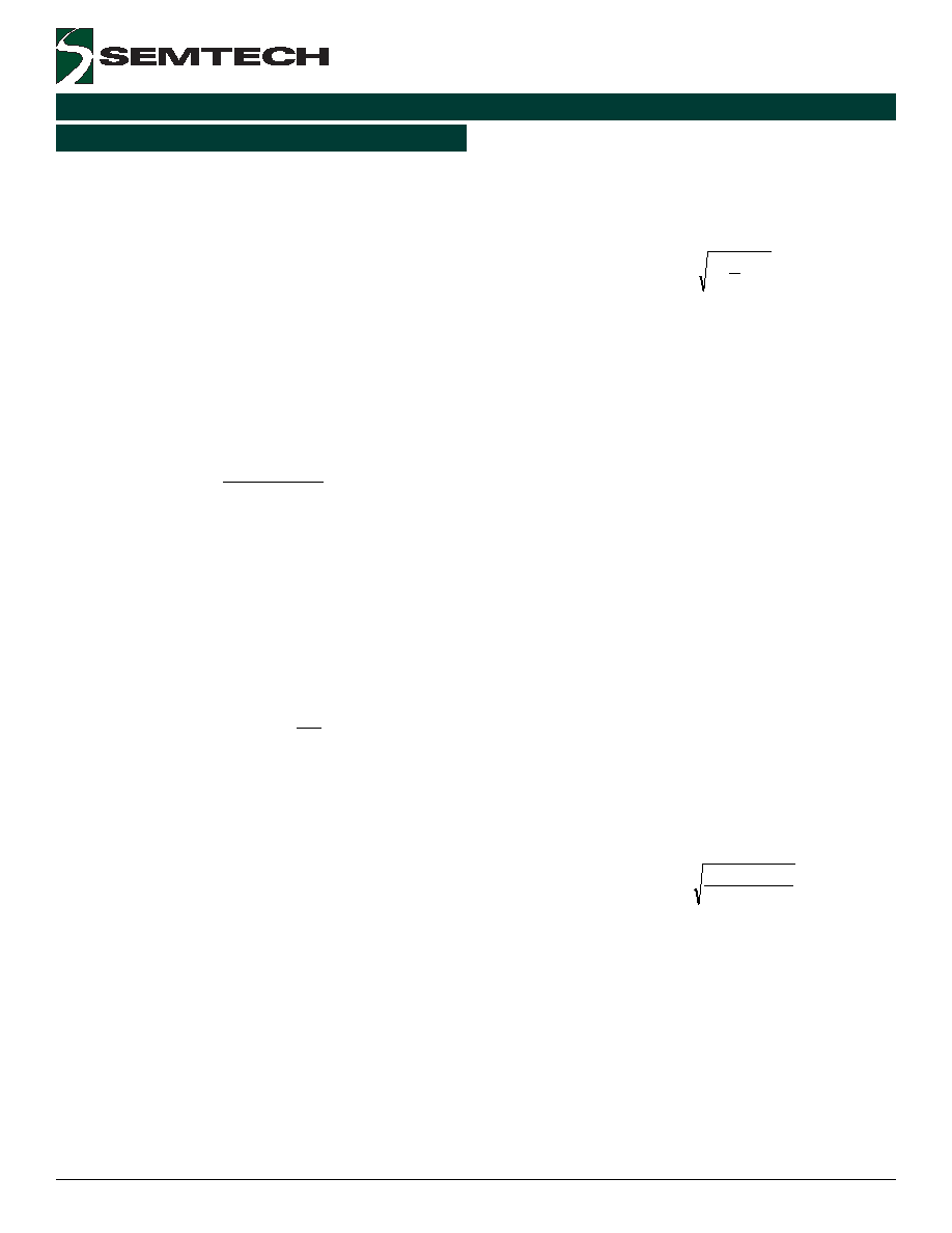
Loop Compensation Design
Assuming the power stage ESR (equivalent series
resistance) zero is an order of magnitude higher than
the closed loop bandwidth, which is typically one tenth of
the switching frequency, the power stage control to output
transfer function with the current loop closed (Ridley
model) for the SC4518 will be as follows:
C
R
1
s
1
R
5
.
2
)
s
(
G
L
L
VD
+
=
Where:
R
L
≠ Load and
C
≠ Output capacitor.
The goal of the compensation design is to shape the loop
to have a high DC gain, high bandwidth, enough phase
margin, and high attenuation for high frequency noises.
Figure 2 gives a typical compensation network which
offers 2 poles and 1 zero to the power stage:
BS
T
1
IN
2
SW
3
GN
D
4
EN
5
FB
6
COMP
7
SYNC
8
SC4518
R2
R1
R3
C4
C
D2
L1
C5
Vout
Figure 2.
Figure 2. Compensation network provides 2 poles and 1
zero.
The compensation network gives the following
characteristics:
2
1
2
m
2
P
Z
1
COMP
R
R
R
g
)
s
1
(
s
s
1
)
s
(
G
+
+
+
=
Where:
5
4
1
C
C
1
+
=
4
3
Z
C
R
1
=
5
4
3
5
4
2
P
C
C
R
C
C
+
=
The loop gain will be given by:
)
s
1
(
)
s
1
(
s
1
s
1
R
R
R
C
R
10
125
.
2
)
s
(
G
)
s
(
G
)
s
(
T
2
P
1
P
Z
2
1
2
4
L
3
VD
COMP
+
+
+
+
=
=
-
Where:
C
R
1
L
1
p
=
One integrator is added at origin to increase the DC gain.
Z
is used to cancel the power stage pole
P1
so that the
loop gain has ≠20dB/dec rate when it reaches 0dB line.
P2
is placed at half switching frequency to reject high
frequency switching noises. Figure 3 gives the asymptotic
diagrams of the power stage with current loop closed
and its loop gain.
C
P2
Z
p1
Loop gain T(s)
Power stage
Figure 3
Figure 3. Asymptotic diagrams of power stage with
current loop closed and its loop gain.

11
2004 Semtech Corp.
www.semtech.com
POWER MANAGEMENT
SC4518
The design guidelines for the SC4518 applications are
as following:
1. Set the loop gain crossover corner frequency
C
for given switching corner frequency
C
=
2
f
c
.
2. Place an integrator at the origin to increase DC and
low frequency gains.
3. Select
Z
such that it is placed at
P1
to obtain a
-20dB/dec rate to go across the 0dB line.
4. Place a high frequency compensator pole
P2
(
P2
=
f
s
) to get the maximum attenuation of
the switching ripple and high frequency noise with
the adequate phase lag at
C.
Layout Guidelines:
In order to achieve optimal electrical and thermal
performance for high frequency converters, special
attention must be paid to the PCB layouts. The goal of
layout optimization is to identify the high di/dt loops and
minimize them. The following guidelines should be used
to ensure proper operation of the converters.
1. A ground plane is suggested to minimize switching
noises and trace losses and maximize heat
transferring.
2. Start the PCB layout by placing the power components
first. Arrange the power circuit to achieve a clean
power flow route. Put all power connections on one
side of the PCB with wide copper filled areas if
possible.
3. The V
IN
bypass capacitor should be placed next to
the V
IN
and GND pins.
4. The trace connecting the feedback resistors to the
output should be short, direct and far away from any
noise sources such as switching node and switching
components.
5. Minimize the loop including input capacitor, the
SC4518 and freewheeling diode D
2
. This loop passes
high di/dt current. Make sure the trace width is wide
enough to reduce copper losses in this loop.
6. Maximize the trace width of the loop connecting the
inductor, freewheeling diode D
2
and the output
capacitor.
7. Connect the ground of the feedback divider and the
compensation components directly to the GND pin
of the SC4518 by using a separate ground trace.
Application Information (Cont.)
8. Connect Pin 4 to a large copper area to remove the
IC heat and increase the power capability of the
SC4518. A few feedthrough holes are required to
connect this large copper area to a ground plane to
further improve the thermal environment of the
SC4518. The traces attached to other pins should
be as wide as possible for the same purpose.
12
2004 Semtech Corp.
www.semtech.com
POWER MANAGEMENT
SC4518
Application Information (Cont.)
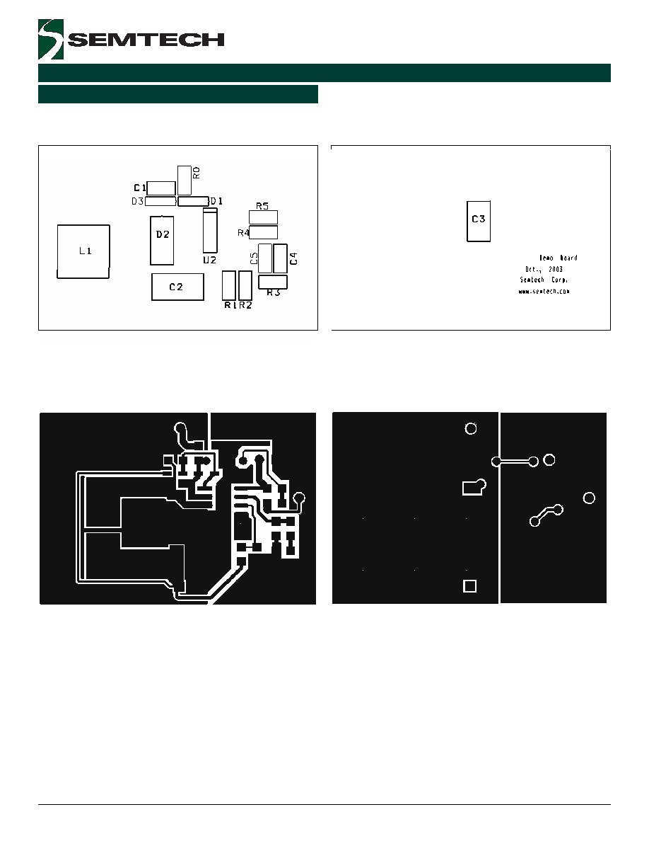
C1
0.22u
SC4518
BS
T
1
IN
2
SW
3
GN
D
4
EN
5
FB
6
COMP
7
SYNC
8
D3
R2
10k
R1
31.6k
R3
8.06k
C4
6.8n
C2
47u
D2
L1
10uH
R4
4.75k
C5
180p
V
I
=12V
V
o
=5V
C3
10u
C1
0.22u
SC4518
BS
T
1
IN
2
SW
3
GN
D
4
EN
5
FB
6
COMP
7
SYNC
8
D3
R2
10k
R1
31.6k
R3
8.06k
C4
6.8n
C2
47u
D2
L1
10uH
R4
4.75k
C5
180p
V
I
=12V
V
o
=5V
C3
10u
Design Example 1. 12V to 5V.
m
e
t
I
y
t
Q
e
c
n
e
r
e
f
e
R
e
u
l
a
V
r
e
r
u
t
c
a
f
u
n
a
M
/.
o
N
t
r
a
P
1
1
1
C
5
0
8
0
,
R
7
X
,
V
5
2
,
F
u
2
2
.
0
X
X
K
4
2
2
Y
5
0
8
0
J
V
:
N
/
P
y
a
h
s
i
V
2
1
2
C
0
1
2
1
,
V
3
.
6
,
F
u
7
4
a
t
a
r
u
M
3
1
3
C
0
1
2
1
,
V
5
2
,
F
u
0
1
c
i
n
o
s
a
n
a
P
4
1
4
C
5
0
8
0
,
V
5
2
,
F
n
8
.
6
y
a
h
s
i
V
5
1
5
C
5
0
8
0
,
V
0
5
,
F
p
0
8
1
y
a
h
s
i
V
6
1
3
D
3
2
3
-
D
O
S
,
S
W
8
4
1
4
N
1
7
1
2
D
3
2
S
S
3
2
S
S
:
N
/
P
d
li
h
c
r
i
a
F
8
1
1
L
H
u
0
1
0
0
1
-
4
7
R
D
:
N
/
P
r
e
p
o
o
C
9
1
1
R
5
0
8
0
,
%
1
,
k
6
.
1
3
E
N
O
Z
T
M
S
0
1
1
2
R
5
0
8
0
.
%
1
,
k
0
1
E
N
O
Z
T
M
S
1
1
1
3
R
5
0
8
0
,
k
6
0
.
8
E
N
O
Z
T
M
S
2
1
1
4
R
5
0
8
0
,
k
5
7
.
4
E
N
O
Z
T
M
S
3
1
1
1
U
8
1
5
4
C
S
T
R
T
S
E
I
8
1
5
4
C
S
:
N
/
P
h
c
e
t
m
e
S
.
e
g
a
k
c
a
p
3
0
6
0
h
ti
w
n
o
i
s
i
c
e
r
p
%
1
e
v
a
h
s
r
o
t
s
i
s
e
r
ll
a
,
d
e
if
i
c
e
p
s
s
s
e
l
n
U
%
0
2
-
/
+
e
r
a
s
r
o
ti
c
a
p
a
c
ll
a
d
n
a
%
1
-
/
+
e
r
a
s
r
o
t
s
i
s
e
R
Bill of Materials
13
2004 Semtech Corp.
www.semtech.com
POWER MANAGEMENT
SC4518
(COMPONENT - TOP)
Application Information (Cont.)
(PCB - TOP)
(PCB - BOTTOM)
(COMPONENT - BOTTOM)
8
8
SC4518
14
2004 Semtech Corp.
www.semtech.com
POWER MANAGEMENT
SC4518
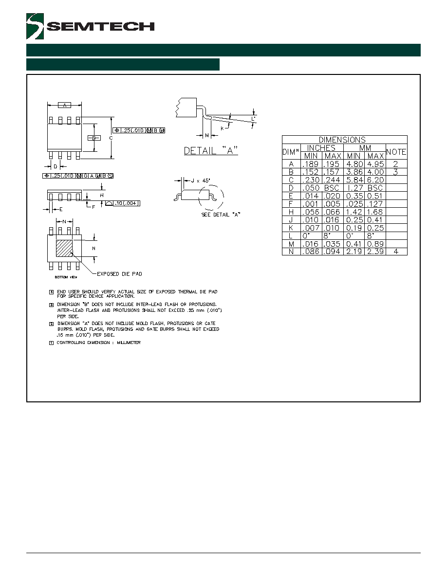
Outline Drawing - SOIC-8L EDP
15
2004 Semtech Corp.
www.semtech.com
POWER MANAGEMENT
SC4518
Contact Information
Semtech Corporation
Power Management Products Division
200 Flynn Road, Camarillo, CA 93012
Phone: (805)498-2111 FAX (805)498-3804
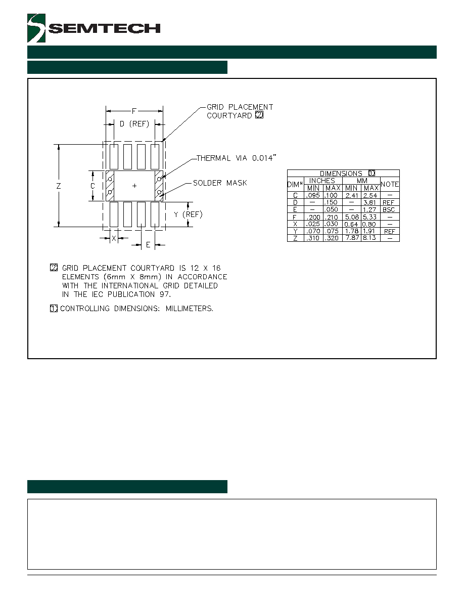
Land Pattern - SOIC-8L EDP