 | –≠–ª–µ–∫—Ç—Ä–æ–Ω–Ω—ã–π –∫–æ–º–ø–æ–Ω–µ–Ω—Ç: SC453 | –°–∫–∞—á–∞—Ç—å:  PDF PDF  ZIP ZIP |

www.semtech.com
1
POWER MANAGEMENT
Portable, VID Programmed Single
Phase Power Supply Controller
SC453
High speed hysteretic controller
Single phase operation
Selectable analog or VID controlled sleep setting
6 bit VID programmable output
Integrated drivers with soft high side turn-on
Programmable soft-start
Programmable boot voltage
Programmable sleep voltage with sleep mode
Under-voltage lock out on VCCA
Over-voltage protection on CORE
Current limit protection on CORE
Thermal protection
Power good fl ag with blanking during
V
CORE
changes
Automatic power save at light load
TSSOP-28 package
December 6, 2005
Description
Features
The SC453 IC is a single chip high-performance Hysteretic
PWM controller. With its integrated SmartDriverTM, it pow-
ers advanced graphics and core processors. It provides
sleep mode and boot voltage support. Automatic "power-
save" is present to prevent negative current flow in the
low-side FET during light loading conditions saving even
more power. The high side driver initially turns on with a
weak drive to reduce ringing, EMI, and capacitive turn-on
of the low side.
A 6-bit DAC, accurate to 0.85%, sets the output voltage
reference, and implements the 0.700V to 1.708V range
required by the processor. The hysteretic converter uses a
comparator without an error amplifier, and therefore pro-
vides the fastest possible transient response, while avoid-
ing the stability issues inherent to classical PWM control-
lers. The DAC is externally slew rate limited to minimize
transient currents and audible noise.
The SC453 operates from 5VDC and also features soft-
start, an open-drain PWRGD signal with power good blank-
ing, and an enable input. Programmable current limiting
shuts down the SC453 after 32 current limit pulses.
Low Power Notebook and Laptop Computers
Embedded Applications
Typical Application Circuit
Applications
Features
PowerStep IVTM and Smart DriverTM are trademarks
of Semtech Corporation.
SC453 Single Phase
Power Supply
Smart
Driver
PWM
Controller
VID Logic
and DAC
VID (5:0)
VIN
V
5
V
CCA
VCORE
0.700V-1.708V

2
© 2005 Semtech Corp.
www.semtech.com
POWER MANAGEMENT
SC453
1
2
R1
10
1
2
R1
2
332
1
2
C7
10
uF
1
2
C1
2
3
30p
F
1
2
C4
10
uF
1
2
R2
0
1
2
R1
0
DNP
1
2
3
4
5
6
L1
0.
5u
H
4
1
2
3
5
6
7
8
D
Q1
IRF
7
8
2
1
1
2
C6
1u
F
1
2
C1
4
4.
7u
F
1
2
C9
1u
F
1
2
+
C1
5
330
u
F
1
2
C2
10
u
F
1
2
C1
3
1n
F
4
1
2
3
5
6
7
8
D
Q2
IR
F
7
8
2
1
1
2
+
C1
8
330
u
F
HY
S
1
2
R4
33
.
2
K
1
2
R
8
1.
8K
+
V
CO
RE
VI
D
4
PG
_
D
E
L
VI
D
0
VI
D
5
PG
#
+
V
CO
RE
VI
D
3
VI
D
1
SL
P
EN
VI
D
2
BG
VI
D
3
VI
D
4
VI
D
5
VI
D
2
VC
C
A
CL
1
2
R1
3
DN
P
DA
C
B
OOT
V
+5
V
PG_
D
EL
DRN
+V
_
I
N
SLP
TG
PG#
BST
BS
T
_
L
DRN
1
TG
2
BST
3
SL
P
4
SL
PV
5
BOOT
V
6
PG#
7
HY
S
8
VI
D
5
9
VI
D
4
10
VI
D
3
11
VI
D
2
12
VI
D
1
13
VI
D
0
14
SS
15
PG
_D
EL
16
CO
RE
17
DA
C
18
GN
D
19
RE
FI
N
20
V
CCA
21
CL
RF
22
CM
P
23
CL
24
EN
25
PGN
D
26
BG
27
V5
28
U1
SC453
SS
CO
R
E
CM
P
VI
D
1
SLP
V
EN
VI
D
0
CS
H
CS
H
CS
H
CS
H
CL
RF
1
2
R3
54
.
9
K
1
2
R7
9
3
1
1
2
C1
0
1n
F
1
2
D2
MB
R
S
1
4
0
L
1
2
C2
2
330
p
F
1
2
C5
10u
F
1
2
R9
0.
00
1
4
1
2
3
5
6
7
8
D
Q4
IR
F
7
8
3
2
1
2
C2
3
1n
F
1
2
C2
1
15n
F
4
1
2
3
5
6
7
8
D
Q3
IR
F
7
8
3
2
1
2
R5
36
.
5
K
1
2
R1
1
0
1
2
C3
10
uF
1
2
+
C1
6
330
uF
1
2
+
C1
7
33
0uF
1
2
R
6
1.
8K
1
2
D1
MB
R
0
5
3
0
1
2
C1
1u
F
1
2
C1
1
27
0p
F
1
2
C8
1
0uF
Reference Design

3
© 2005 Semtech Corp.
www.semtech.com
POWER
MANAGEMENT
SC453
Absolute Maximum Ratings
Exceeding the specifi cations below may result in permanent damage to the device or device malfunction. Operation outside of the parameters specifi ed in the
Electrical Characteristics section is not implied.
Unless otherwise specifi ed: V
IN
= 15V, V
CCA
= 5V, and V5 = 5V.
(1) Calculated from package in still air, mounted to 3" x 4.5", 4 layer FR4 PCB.
(2) Tested according to JEDEC standard JESD22-A114-B.
Parameter
Symbol
Conditions
Min
Max
Units
Supply Voltages
V
CCA,
V
5
-0.3
7
V
Input and Output Voltages
VSLPV, V SLP, V VID [0.5], V DAC, V REFIN,
V CMP, V HYS, V CORE, V CL, V CLRF, V PG#,
V BOOTV, V SS, V GND, V BG, V CLSET
-0.3
V
CCA
+0.3
V
EN
V
EN
7
V
BST to PGND
Static
-0.3
36
V
BST to PGND
Transicent < 100ns
40
V
BST to DRN
-0.3
7
V
DRN to PGND
Static
-2
30
V
DRN to PGND
Transient < 100ns
-5
34
V
TG
T
STG
-2
BST
+0.3
V
PGND to AGND
-0.3
0.3
V
Thermal Resistance
Junction to Ambient
JA
TSSOP-28
70
∞C/W
Thermal Resistance
Junction to Case
JC
TSSOP-28
20
∞C/W
Lead Temperature
(Soldering) 10s
T
LEAD
TSSOP-28
TBD
∞C
Peak IR Refl ow
Temperature 10 - 40s
T
PKG
TSSOP-28
260
∞C
Parameter
Symbol
Conditions
Min
Typ
Max
Units
Supply (V
IN
, V
CCA
, V
5
)
V
IN
Supply
Voltage Range
V
IN
3.0
25
V
V
5
Supply
Voltage Range
V
5
4.3
5.0
6.0
V
V
CCA
Voltage Range
V
CCA
4.5
5.0
6.0
V
V
CCA
Quiescent Current
I
CCQ
EN is low
10
A
EN is high in UVLO
400
A
Absolute Maximum Ratings
Electrical Characteristics

4
© 2005 Semtech Corp.
www.semtech.com
POWER MANAGEMENT
SC453
Parameter
Symbol
Conditions
Min
Typ
Max
Units
V
CCA
Operating Current
I
CC
5
mA
Under-Voltage Lockout Circuits (V
CCA
, V
5
)
Threshold (V
CCA
falling)
V
HCCA
3.47
3.70
3.93
V
V
CCA
Hysteresis
V
HYST CCA
190
mV
Threshold (V
5
falling)
V
HV5
3.85
4.00
4.25
V
V
5
Hysteresis
V
HYST V5
210
mV
Fixed Over-Voltage Protection (CORE)
Threshold
(CORE Rising)
V
TH CORE
FIXED
1.95
2.00
2.05
V
Enable Input (EN)
Input High
V
iH (EN)
2
V
Input Low
V
iL
(EN)
0.8
V
V
CORE
Power Good Generator (PG_DEL, PG#)
Core Input Threshold
V
TH CORE
V
DAC
= 0.6 - 1.75V
Note: during
UVLO, the
output level of
this signal is
undefi ned
Upper Threshold
1.1*
V
DAC
1.15*
V
DAC
V
Lower Threshold
0.86*
V
DAC
0.9*
V
DAC
Hysteresis
1
%
PG# Output Voltage
V
PG#
Pulled up with
external 680
resistor to
V
PULL-UP
V
CORE
= V
DAC
0.4
V
Either V
CORE
< 0.88*V
DAC
,
or, V
CORE
> 1.12*V
DAC
0.95*
V
PULL-UP
EN is low or EN is high
but UVLO condition
0.95*
V
PULL-UP
PG_DEL
Output Voltage
V
PG_DEL
V
CORE
= V
DAC
pulled-up with external
680 resistor to V
PULL-UP
1.2V
0.95*
V
PULL-UP
V
Either V
CORE
< 0.88*V
DAC
,
or, V
CORE
> 1.12*V
DAC
0.4
EN is low or EN is high
but UVLO condition
0.8
PG_DEL Delay
(at start-up)
Measured from PG# assertion
1007
Clocks
Electrical Characteristics (Cont.)

5
© 2005 Semtech Corp.
www.semtech.com
POWER
MANAGEMENT
SC453
Parameter
Symbol
Conditions
Min
Typ
Max
Units
Soft-Start & DAC Slew (SS)
Soft-Start/DAC
Slew Current
Note:
SS cap is not discharged
until EN goes low or
UVLO cuts in. To enable
the converter, SS has to
drop below V
SS_EN
.
I
SS
Discharge (sink) Current
5
10
mA
Soft-Start transition 0 < T
A
< 85∞C,
- 40 < T
A
< 85∞ C
7.5
10.5
16
A
Sleep Exit, 0 < T
A
< 85∞C
204
256
310
Sleep Exit, -40 < T
A
< 85∞C
180
240
320
VID Transition, 0 < T
A
< 85∞C
102
128
155
VID Transition, -40 < T
A
< 85∞C
90
120
160
Soft-Start
Enable Threshold
V
SS_EN
40
100
mV
DAC (VID [5:0])
VID Input Threshold
V
iH_VID
0.55
V
V
iL_VID
0.45
DAC Output
Voltage Accuracy
V
DAC_ERR
0∞ < T
A
< 85∞C, VID [5:0] = 000000
"111111(1.708V" 0.812V)
-0.85
+0.85
%
-25∞C < T
A
< 85∞C, VID [5:0] = 000000
"111111 (1.708V" 0.700V)
-2.0
+2.0
%
Boot Voltage (BOOTV)
Input Voltage Offset
V
BOOTV
-
V
DAC
BOOTV = 1.2V
|±3|
%
BOOT Delay Time
(1)
TBOOT
10
35
s
Sleep (SLP, SLPV)
Input Voltage Offset
V
SLPV
-V
DAC
SLPV = 0.8V
|±3|
%
SLP Logic Threshold
V
iH_SLP
2
V
V
iL_SLP
0.8
CORE Comparator (CMP, REFIN, HYS)
Input Bias Current
I
REFIN
V
REFIN
= 1.3V
|±2|
A
Input Voltage Offset
V
CMP
-
V
REFIN
|±1.5|
|±3|
mV
Electrical Characteristics (Cont.)

6
© 2005 Semtech Corp.
www.semtech.com
POWER MANAGEMENT
SC453
Parameter
Symbol
Conditions
Min
Typ
Max
Units
CORE Comparator (CMP, REFIN, HYS) (Cont.)
Hysteresis Setting
Current SLP = low
I
CMP
R
HYS
= 17K
V
CMP
< V
REFIN
-110
-100
-90
A
V
CMP
> V
REFIN
90
100
110
R
HYS
= 170K
V
CMP
< V
REFIN
-7
-10
-13
V
CMP
> V
REFIN
7
10
13
Hysteresis Setting
Current SLP = high
I
SLP_
I
CMP
R
HYS
= 17K
V
CMP
< V
REFIN
-83
-73
-63
A
V
CMP
> V
REFIN
63
73
83
Current Limit Comparator (CL, CLRF, HYS)
Input Bias Current
I
CL
V
CL1, 2
= 1.3V
|±2|
A
Input Voltage Offset
V
CL
-
V
CLRF
|±3|
|±5|
mV
Current Limit Setting
Current SLP = low
I
CLRF
R
HYS
= 17K
V
CL
< V
CLRF
150
200
250
A
V
CL
> V
CLRF
250
300
350
R
HYS
= 170K
V
CL
< V
CLRF
15
20
25
V
CL
> V
CLRF
25
30
35
Current Limit Setting
Current SLP = high
I
SLP_CLRF
R
HYS
= 17K
V
CL
< V
CLRF
120
150
180
A
V
CL
> V
CLRF
195
230
265
Zero-Crossing (Powersave) Comparators (CL, CORE)
Offset
V
CL
-
V
CORE
|±5|
mV
High Side Driver (TG)
Peak Output Current
(1)
I
pkh
1.5
A
Output Resistance
R
SRC_TG
I = 100mA,
V
BST
-V
DRN
= 5V
V
DRN
< 1V
4.2
V
DRN
> 1V
1
4
R
SINK_TG
I = 100mA, V
BST
-V
DRN
= 5V
0.7
1.4
Rise Time
(1)
tr
TG
C
TG
= 3nF, V
BST
-V
DRN
= 5V
60
ns
Fall Time
(1)
tf
TG
C
TG
= 3nF, V
BST
-V
DRN
= 5V
36
ns
Electrical Characteristics (Cont.)

7
© 2005 Semtech Corp.
www.semtech.com
POWER
MANAGEMENT
SC453
Parameter
Symbol
Conditions
Min
Typ
Max
Units
High Side Driver (Cont.)
Propagation Delay TG
Going High
(1)
tpdh
TG
CMP crossing REFIN to 10%
point of TG, C
TG
= 3nF,
BG = 0V
45
ns
Propagation Delay TG
Going Low
(1)
tpdl
TG
CMP crossing REFIN to 90%
point of TG, C
TG
= 3nF
45
ns
Shoot-thru Protection
Delay Time
(1)
tspd
21
30
39
ns
Low Side Driver (BG)
Peak Output Current
(1)
I
pkl
3
A
Output Resistance
R
SRC_BG
I = 100mA, V5 = 5V
1.0
2.6
R
SINK_BG
0.5
1.2
Rise Time
(1)
tr
BG
C
BG
= 3nF, V5 = 5V
25
ns
Fall Time
(1)
tf
BG
C
TG
= 3nF, V = 5V
15
ns
Propagation Delay TG
Going High
(1)
tpdh
BG
CMP crossing REFIN to 10%
point of BG, C
BG
= 3nF, DRN = 0V
35
ns
Propagation Delay TG
Going Low
(1)
tpdl
BG
CMP crossing REFIN to 90%
point of TG, C
TG
= 3nF, DRN = 0V
35
ns
Notes:
1) Guaranteed by design.
Electrical Characteristics (Cont.)

8
© 2005 Semtech Corp.
www.semtech.com
POWER MANAGEMENT
SC453
Device
Package
Temp Range(T
J
)
SC453TSTRT
TSSOP-28
-40∞C to + 125∞C
Notes:
1. Only available in tape and reel packaging. A reel contains
2500 devices.
2. Lead-free package compliant with J-STD-020B. Qualifi ed
to support maximum IR refl ow temperature of 260∞C for 30
seconds.
3. This device is ESD sensitive. Use of standard ESD handling
precautions is required.
4. All parameters subject to change without notice.
5. Lead-free product. This product is fully WEEE and RoHS
compliant.
Pin#
Pin Name
Pin Function
1
DRN
This pin connects to the junction of the switching and synchronous MOSFETs.
2
TG
Output gate drive for the switching (high-side) MOSFET.
3
BST
Bootstrap pin. A capacitor is connected between BST and DRN pins to develop
the fl oating bootstrap voltage for the high-side MOSFET.
4
SLP
Sleep logic input signal.
5
SLPV
Connect this pin to V
CCA
to select "VID Sleep Mode". Otherwise, "SLPV Sleep Mode"
is selected and the voltage on this pin sets the DAC output during sleep.
6
BOOTV
The voltage on this pin sets the BOOT-Up voltage.
7
PG#
Start clock indicator - open drain output. Active low.
8
HYS
Core Comparator Hysteresis. Connect to ground thru an external resistor called R
HYS
.
Hysteresis current is established by an internal V
REF
voltage, 1.7V, divided by R
HYS
.
9
VID5
VID most signifi cant bit main controller voltage programming DAC input.
10
VID4
VID input.
Pin Confi guration
Ordering Information
Pin Descriptions
1
2
3
4
5
6
7
8
V5
DRN
TOP VIEW
(28 Pin TSSOP)
27
28
15
16
BG
TG
PGND
BST
EN
SLP
CL
SLPV
CMP
BOOTV
CLRF
PG#
VCCA
HYS
9
10
22
REFIN
VID5
GND
VID4
21
18
17
19
20
11
12
24
DAC
VID3
CORE
VID2
23
25
26
13
14
PG_DEL
VID1
SS
VID0
9
© 2005 Semtech Corp.
www.semtech.com
POWER
MANAGEMENT
SC453
Pin Confi guration
Pin Descriptions (Cont.)
Pin#
Pin Name
Pin Function
11
VID3
VID input.
12
VID2
VID input.
13
VID1
VID input.
14
VID0
VID least signifi cant bit main controller voltage programming DAC input.
15
SS
Soft-start. An external cap defi nes the soft-start ramp.
16
PG_DEL
Delayed power good - open drain output. When the Main Converter Output approaches
and stays within ± 14% of the VID_DAC setting, and the t
CPU_PWRGD
period has terminated.
This signal is pulled high by an external resistor.
17
CORE
Main CORE converter output feedback to the power good generator. A small RC fi lter
should be used to fi lter out any HF component to prevent faulty trip condition.
18
DAC
Main controller digital-to-analog output.
19
GND
Analog ground.
20
REFIN
Core Comparator reference input pin. Connect to DAC.
21
VCCA
5V supply for precision analog circuitry.
22
CLRF
Current limit reference input pin
23
CMP
Core Comparator input pin.
24
CL
Current limit input pin.
25
EN
Enable - active high. This is capable of accepting a 5.0V signal level.
26
PGND
Power ground. Connect to the synchronous FET power ground.
27
BG
Output drive for the synchronous (low-side) FET.
28
V5
5VDC supply for the driver. A capacitor should be connected from V5 to GND.

10
© 2005 Semtech Corp.
www.semtech.com
POWER MANAGEMENT
SC453
Block Diagram
`
`
VID/SLPV Sleep Mode Detect
SLPV
BOOTV
SLP
REFIN
PG_DEL
PG#
```

11
© 2005 Semtech Corp.
www.semtech.com
POWER
MANAGEMENT
SC453
Applications Information (Cont.)
SUPPLY, BIAS, UVLO, POWER GOOD GENERATOR
Supply
The chip is optimized to operate from a 5V ± 5% rail but
also designed to work up to 6V maximum supply voltage.
Under-Voltage Lock-Out Circuit
The Under-Voltage Lock-Out Circuit consists of compara-
tors which monitor the VCCA and V5 voltage levels. The
SC453 is in UVLO mode while either supply has not
ramped above the upper threshold or has dropped below
the lower threshold. During UVLO, the external FETs are
held off, tri-stating the output (DRN).
Over-Voltage Protection
If the CORE voltage is greater than +14% of the DAC (i.e.,
out of the power good window), the SC453 will latch off
and hold the low-side driver on permanently. Either the
power or EN must be recycled to clear the latch. The latch
is disabled during soft-start and VID/Sleep transitions.
For safety, the latch is enabled if the CORE voltage ex-
ceeds 2V even during VID/Sleep transitions.
Thermal Shutdown
The device will be disabled and latched off when the inter-
nal junction temperature reaches approximately 160∞C.
Either the power or EN must be recycled to clear the
latch.
Band Gap Reference
A ± 0.85% precision Band Gap reference acts as the in-
ternal reference voltage standard of the chip, which all
critical biasing voltages and currents are derived from.
All
references to VREF in the equations to follow will assume
VREF = 1.7V.
Precision DAC
This 6-bit digital-to-analog converter (DAC) serves as the
programmable reference source of the Core Comparator.
Programming is accomplished by logic voltage levels ap-
plied to the DAC inputs. The VID code vs. the DAC output
is shown in the following table. The accuracy of the VID
/DAC is maintained on the same level as the Band Gap
reference.
VID
V
DAC
VID
V
DAC
5
4
3
2
1
0
V
5
4
3
2
1
0
V
0
0
0
0
0
0
1.708
1
0
0
0
0
0
1.196
0
0
0
0
0
1
1.692
1
0
0
0
0
1
1.180
0
0
0
0
1
0
1.676
1
0
0
0
1
0
1.164
0
0
0
0
1
1
1.660
1
0
0
0
1
1
1.148
0
0
0
1
0
0
1.644
1
0
0
1
0
0
1.132
0
0
0
1
0
1
1.628
1
0
0
1
0
1
1.116
0
0
0
1
1
0
1.612
1
0
0
1
1
0
1.100
0
0
0
1
1
1
1.596
1
0
0
1
1
1
1.084
0
0
1
0
0
0
1.580
1
0
1
0
0
0
1.068
0
0
1
0
0
1
1.564
1
0
1
0
0
1
1.052
0
0
1
0
1
0
1.548
1
0
1
0
1
0
1.036
0
0
1
0
1
1
1.532
1
0
1
0
1
1
1.020
0
0
1
1
0
0
1.516
1
0
1
1
0
0
1.004
0
0
1
1
0
1
1.500
1
0
1
1
0
1
0.988
0
0
1
1
1
0
1.484
1
0
1
1
1
0
0.972
0
0
1
1
1
1
1.468
1
0
1
1
1
1
0.956
0
1
0
0
0
0
1.452
1
1
0
0
0
0
0.940
0
1
0
0
0
1
1.436
1
1
0
0
0
1
0.924
0
1
0
0
1
0
1.420
1
1
0
0
1
0
0.908
0
1
0
0
1
1
1.404
1
1
0
0
1
1
0.892
0
1
0
1
0
0
1.388
1
1
0
1
0
0
0.876
0
1
0
1
0
1
1.372
1
1
0
1
0
1
0.860
0
1
0
1
1
0
1.356
1
1
0
1
1
0
0.844
0
1
0
1
1
1
1.340
1
1
0
1
1
1
0.828
0
1
1
0
0
0
1.324
1
1
1
0
0
0
0.812
0
1
1
0
0
1
1.308
1
1
1
0
0
1
0.796
0
1
1
0
1
0
1.292
1
1
1
0
1
0
0.780
0
1
1
0
1
1
1.276
1
1
1
0
1
1
0.764
0
1
1
1
0
0
1.260
1
1
1
1
0
0
0.748
0
1
1
1
0
1
1.244
1
1
1
1
0
1
0.732
0
1
1
1
1
0
1.228
1
1
1
1
1
0
0.716
0
1
1
1
1
1
1.212
1
1
1
1
1
1
0.700

12
© 2005 Semtech Corp.
www.semtech.com
POWER MANAGEMENT
SC453
DAC Slew Control
The output of the DAC will slew at a rate defi ned by the
current in the SS pin and the capacitor applied externally
to the SS pin. The slew rate (charge current) applied de-
pends on which mode (soft-start, VID or sleep transition)
is in effect. The SS capacitor together with the DAC ca-
pacitor will determine the stability of the DAC, a 1nF ca-
pacitor is recommended for the DAC pin.
Blanking During VID Changes
On any VID change or Sleep change, the PG# and PG_
DEL signals are blanked for 62 switching cycles to prevent
glitching during the transition.
Sleep Function
In sleep mode, the DAC output is set by the voltage on
the SLPV pin when the SLP pin is held high. In "VID Sleep"
mode, the DAC output is set by the VID bits when SLP is
held high. During sleep, the hysteresis and current limit
hysteresis currents are reduced to 70% of their nominal
values.
SLPV/VID Sleep Mode
By default, the controller is in "SLPV controlled Sleep"
mode. In this mode, the voltage applied to the SLPV pin
appears at the DAC output when SLP is asserted.
By holding the SLPV pin at VCCA during start-up, "VID con-
trolled sleep" mode is engaged. In this mode, the DAC out-
put continues to be set by the VID inputs even when SLP
is asserted.
CORE CONVERTER CONTROLLER
Core Comparator
This is an ultra-fast hysteretic comparator with a typical
propagation delay of about 20ns at a 20mV overdrive.
Hysteresis is generated by the current set at the HYS pin
impressed upon an external resistor connected to the
CMP pin.
Current Limit Comparator
The Current Limit Comparator monitors the core converter
output current and turns off the high side FETs when the
current exceeds the upper current limit threshold, VHCL
and is re-enabled only if the phase current drops below
the lower current limit threshold, VLCL.
The current is
sensed by monitoring the voltage drop across the current
sense resistor, RCS connected in series with the core con-
verter inductor. VHCL and VLCL are fi xed by the current
set at the HYS pin impressed upon an external resistor
connected to the CLRF pin.
Current Limit Latch
If the CORE voltage goes lower than 14% below the VID
(i.e., out of the power good window), then sustained cur-
rent limiting (32 current limit pulses) will cause the part
to permanently latch off. The latch is inhibited during soft-
start.
Core Converter Soft-Start Timer
This block controls the start-up ramp time of the CORE
voltage up to the boot voltage. The primary purpose is to
reduce the initial in-rush current on the core input voltage
(battery) rail.
Cycle-by-Cycle Power-Save
A zero crossing comparator detects when the currents
through the external sense resistor reduces to zero. When
the current in the external sense resistor reaches zero,
the bottom FET is latched off. The latch is reset when the
controller decides to switch on the top FET. This prevents
excessive switching at light loads and hence saves switch-
ing power losses.
Applications Information (Cont.)

13
© 2005 Semtech Corp.
www.semtech.com
POWER
MANAGEMENT
SC453
Applications Information (Cont.)
PG# Output
This is an open-drain output and should be pulled up ex-
ternally. This signal is asserted (pulled low) by the SC453
whenever the core voltage is within ±14% of the VID
programmed value. If the chip is disabled or enabled in
UVLO, then PG# is de-asserted. During start-up PG# re-
mains de-asserted until the core voltage has reached the
defi ned boot voltage and remains there for the BOOT pe-
riod (10S minimum). This signal is forced low (asserted)
during VID and sleep transitions.
PG_DEL Output
This signal is delayed a minimum of 3mS from fi rst as-
sertion of the PG# signal. This is an open drain output
and should be pulled up externally. This signal is asserted
(open drain) by the SC453 whenever the core is within
±14% of the VID programmed value. If the chip is disabled
or enabled in UVLO, then PG_DEL is de-asserted. The sig-
nal is forced high (open drain) during VID and sleep transi-
tions.
Start-Up and Sequencing
On start-up, V
CORE
ramps to the boot voltage set by the
BOOTV pin irrespective of the status of the VID pins. After
a minimum of 10s, PG# asserts, and V
CORE
responds to
the VID inputs. The controller will then count 1007 switch-
ing cycles before asserting PG_DEL.
Summary of Fault Conditions
Driver Timing Diagram
CMP
BG
TG
CMPRF
tf
tpdl
tpdh tr
tpdl tf tspd
tr
TG
TG
TG
BG
BG
BG
BG
tpdh
TG
(4)
(4)
Note (4): subtract a typical value of 17ns for the core comparator delay since this parameter is specifi ed from a CMP edge.
Protection Mode
Latched?
When Active
Driver Status
SS Pin Status
Supply UVLO (VCCA, V5)
No
Always
All low
Low
32 Cycle Current Limit
Yes
SS has terminated and PGDEL is low
TG low
Sawtooth
114% V
CORE
OVP
Yes
SS has terminated and PGDEL is low
BG high
High
2.0V
CORE
OVP
Yes
Always
BG high
High
Thermal Shutdown
Yes
Always
BG, TG low
High
REFIN

14
© 2005 Semtech Corp.
www.semtech.com
POWER MANAGEMENT
SC453
Applications Information (Cont.)
DESIGN PROCEDURE
Step 1: Defi ne Constants
Maximum input voltage
Minimum input voltage
Maximum load current,
highest
output
voltage
Leakage current, highest
output
voltage
The highest V
CORE
voltage
The lowest V
CORE
voltage
SC453 Internal reference voltage
Output capacitance per cap
ESR per cap
Current sense resistor
Parasitic resistance from the
current sense resistor to the
processor
Voltage droop allowed for a low
current to high current transient
Voltage rise allowed for a high
current to low current transient
Desired maximum output ripple
Step 2: Output Inductor and Capacitor Selection
The SC453 has "passive" droop. The voltage at full load is
less than the DAC voltage by the voltage drop across the
current sense resistor and any PCB copper losses from
the sense resistor to the processor socket. The steady-
state voltage at full load is:
V
MAX_FL
V
MAX_NL
R
CS
R
CU
+
(
)
I
MAX_FL
-
:=
V
MAX_FL
1.182 V
=
Output capacitance and ESR values are a function of
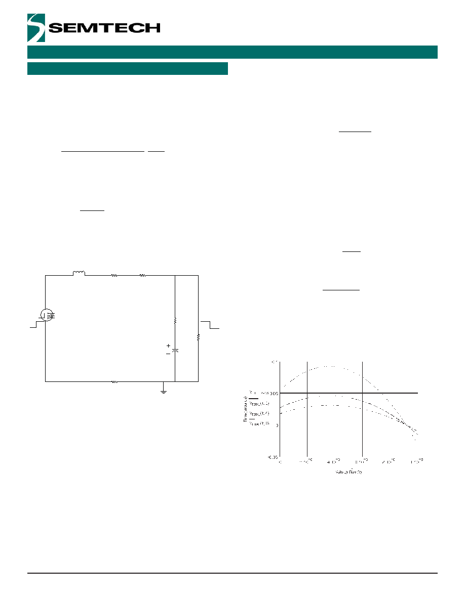
transient requirements and output inductor value. Figure
1 illustrates the response of a hysteretic converter to a
positive transient. In a hysteretic converter with passive
droop, like the SC453, two conditions determine if you
meet the positive transient requirements.
A.
ESR
V
POS_TRANS
I
MAX_FL
I
LKGMAX
-
(
)
B.
V
NEG_TRANS
deltaV C
OUT
( )
Figure 1 - Hysteretic Converter Response to a
Positive Transient
The fi rst condition is easy to see; if the ESR is too high, the
transient response will fail.
V
INMAX
20V
:=
V
INMIN
8V
:=
I
MAX_FL
20A
:=
I
LKGMAX
5A
:=
V
MAX_NL
1.212V
:=
V
MIN_NL
0.956 V
:=
V
REF
1.7V
:=
C
OUT
330
F
:=
R
ESR
6m
:=
R
CS
1m
:=
R
CU
0.5m
:=
V
POS_TRANS
50mV
:=
V
NEG_TRANS
50mV
:=
V
RIPPLE
20m V
:=

15
© 2005 Semtech Corp.
www.semtech.com
POWER
MANAGEMENT
SC453
In the second condition, because the hysteretic converter
responds in < 100ns, the capacitor does not droop very
far before the inductor current starts ramping up. (This is
not true of control schemes where time constants in the
error amplifi er cause delays.) Once the inductor current
starts to rise, the increasing V of the capacitor is offset
by reduced V from the ESR, so V is constant. If the V
due to the charge taken from the capacitor before the in-
ductor current reaches the load current (note the shaded
area on the graph) is less than VPOS_TRANS, then the
transient response passes.
Since the highest output voltage has the most severe re-
quirements, any other modes are satisfi ed by a design op-
timized for the highest output voltage.
C.
For the second condition, we need to know the inductor
value, which is a function of the highest desired switching
frequency. The maximum frequency occurs at the high-
est input voltage. As a reasonable compromise between
effi ciency and component size, a maximum switching fre-
quency of 350kHz is desired.
D.
E.
F.
Based on the following four factors: 1) minimum induc-
tance requirement; 2) device availability at the time we
designed the evaluation board; 3) low DCR ; 4) height and
package size consideration. Keep in mind, the choice you
make should be based upon the requirement of the con-
verter design, including minimum inductance, minimum
saturation current, effi ciency, foot area, maximum allow-
able height, and of course, device availability. In the cur-
rent demo board design,
G.
This value of inductance is required up to maximum load.
Inductors with a "swinging choke" characteristic, where
the zero current value of inductance is much less than the
full load current inductance can be used, as long as the
above restriction is met. Then, the worst-case (low input
voltage) response time (the time for the current to reach
the new transient value) is:
H.
Add ~100ns for the propagation delay from a change at
the output to the MOSFET switch turning on in reaction.
Since the shaded area is triangular, the total charge taken
out of the capacitor = (dI / dt) / 2. Q = C / dV = (dI / dt) /
2, therefore;
I.
C
MINP
I
MAX_FL
I
LKGMAX
-
(
)
dT
1 10
7
-
sec
+
(
)
V
POS_TRANS
:=
C
MINP
4.278
10
4
-
◊
F
=
This condition applies only to the positive transient.
L
MIN
d
MIN
V
INMAX
V
MAX_NL
-
(
)
ESR
MAX
R
CS
+
(
)
F
S
V
RIPPLE
ESR
MAX
R
CS
+
ESR
MAX
:=
L
MIN
5.422
10
7
-
◊
H
=
d
MIN
V
MAX_NL
V
INMAX
:=
Applications Information (Cont.)
ESR
MAX
V
POS_TRANS
I
MAX_FL
I
LKGMAX
-
(
)
:=
ESR
MAX
3.333
10
3
-
◊
=
L
1
0.60
H
:=
F
S
350K Hz
:=
dT
L
1
I
MAX_FL
I
LKGMAX
-
(
)
V
INMIN
V
MAX_NL
-
:=
dT 1.326
10
6
-
◊
s
=
16
© 2005 Semtech Corp.
www.semtech.com
POWER MANAGEMENT
SC453
LOAD RELEASE
The worst-case for the transient load release to happen is
when the hysteresis has just reached the maximum, (i.e.,
the high-side switch has just turned of); at this time the
inductor has reached its peak current.
I
RIPPLE
V
INMAX
V
MAX_FL
-
(
)
d
MIN
L
1
F
S
L
1
L
MIN
:=
I
t0
I
MAX_FL
I
RIPPLE
2
+
:=
Load is stepping from high to low.
Immediately after the load steps down from I
MAX
to I
MIN
, the
high side FET is turned off, and the bottom FET is turned
on after the dead time. We assume for the worst-case
condition, at t = 0, the output inductor is sitting at its max-
imum; after t = 0, the inductor discharges at a rate equal
to V
FL
/ L.
(without the consideration of the secondary or-
der effect, such as, Rds_on drop, current sense resistor
and copper losses). The energy released from the output
inductor during load step-down,
charges
the output ca-
pacitors and is dissipated through the following means:
Rds_on, Rcs, Rcu, Rcu_rt, ESR of the output capacitors
and load.
Applications Information (Cont.)
Since the output inductor is discharging at a fi xed rate,
there are two terms contributing to the increase of the
voltage on the output capacitors: 1) is due to the ESR of
the output capacitor; 2) is due to the added charge con-
tributed by the inductor current.
J.
V
ESR
t N
CAP
,
(
)
I
CAP
t
( )
R
ESR
N
CAP
:=
K.
dV
CAP
t N
CAP
,
(
)
I
CAP
t
( ) t
C
OUT
N
CAP
:=
L.
V
TOTAL
t N
CAP
,
(
)
V
ESR
t N
CAP
,
(
)
dV
CAP
t N
CAP
,
(
)
+
:=
The chart above shows the system response for the ca-
pacitors defi ned in Step 1 and the chart to follow shows
the details of the response for the chosen number of out-
put capactors.
L
R
DS
R
CU
ESR_eq
I
MAX
I
MIN
Cout_eq
Rcu_rt
Rds_ON
BG
R_LOAD
t
0 10n s
,
10
s
..
:=
I
L
t
( )
I
t0
V
MAX_FL
t
L
1
-
:=
I
CAP
t
( )
I
L
t
( )
I
LKGMAX
-
:=
I
RIPPLE
6.01 A
=
I
t0
23.005 A
=

17
© 2005 Semtech Corp.
www.semtech.com
POWER
MANAGEMENT
SC453
Applications Information (Cont.)
Step 3: Setting RHYS
The next step is to calculate R
HYS
. Since the SC453 is a
hysteretic controller, it regulates the amount of output
ripple according to a hysteresis value set by R
HYS
. The de-
signer must therefore decide upon the amount of desired
output ripple, and then set R
HYS
accordingly.
The hysteresis controls the amount of ripple at the point
of regulation, which is the point between the inductor and
the current sense resistor. The amount of ripple at the
output is defi ned by the current sense resistor and the
output cap, ESR. This factor is taken into account in the
equation shown below relating V
RIPPLE
to V
HYS
.
To achieve tight accuracy, it is recommended that the out-
put ripple be set to 20mV peak-to-peak.
ESR
R
ESR
N
CAP
:=
ESR 1.5
10
3
-
◊
=
V
RIPPLE
0.02 V
=
M.
V
HYS
V
RIPPLE
R
CS
ESR
+
(
)
ESR
:=
V
HYS
0.033 V
=
V
HYS
is created by a current source, I
HYS
, through R9 (see
the diagram below). The current source value is con-
trolled via R
HYS
. For simplicity it is easier to select a value
for R7 (the resistor in series with the CMP pin) fi rst, and
then calculate R
HYS
, as follows:
N.
R
7
1K
:=
.
R
HYS
2 V
REF
V
HYS
R
7
:=
R
HYS
102.0 K
=
In the SC453 application circuit, R
HYS
consists of three re-
sistors (R3, R4 and R5). These resistors also form the
dividers for BOOTV and SLPV. Note also that depending
on circuit layout and parasitics, R
HYS
may have to be ad-
justed slightly to obtain optimum performance. (We will
come back to calculate the above resistors after we set
the PBOOT and Deeper Sleep voltages). To increase hys-
teresis without having to change the divider resistors, a
fourth resistor (R14), can be added. Additional hysteresis
is needed when inductances in the current sense paths
cause additional signal that add to the resistive signal,
limiting the accuracy of the calculations.
R14
HYS
BOOTV
SLPV
R5
R4
R3
SC453

18
© 2005 Semtech Corp.
www.semtech.com
POWER MANAGEMENT
SC453
Step 4: BOOTV Design
The boot-up voltage for V
CORE
is set at 1.2V. For the SC453
typical application circuit, R3, R4, and R5 form a voltage
divider off V
REF
and are used to set the boot voltage. For
simplicity, we defi ne R
BOOT
: = R3 + R4.
V
BOOT
1.2V
:=
O.
R
HYS
1
1
R
25
1
R
BOOT
R
5
+
+
:=
P.
R
BOOT
V
BOOT
R
5
V
REF
V
BOOT
-
:=
Step 5: Sleep Voltage Design
The sleep voltage is set at 0.750V nominally using the R3
- R4 - R5 divider.
Q.
V
SLP
0.750V
:=
R3, R4 and R5 are calculated using a matrix to solve the
simultaneous equations. R14 is set at 1M as a place-
holder:
R
14
1000 K
:=
M
x
1
1
1
1
1
V
SLP
1
-
V
REF
V
SLP
-
1
V
BOOT
V
REF
V
BOOT
-
-
V
SLP
1
-
V
REF
V
SLP
-
:=
Applications Information (Cont.)
From the standard 1% resistor value table, we choose
the following values according to the calculation results:
R5 = 33.2K.
R4 = 30.1K
R3 = 49.9K
Step 6: Current Limit Calculation
Setting the threshold for current limit is a relatively
straightforward process. To do this we must calculate the
peak current based on the maximum DC value plus the
worst-case ripple current. The following calculations apply
for a single phase. Worst-case ripple occurs at the high-
est input voltage. Since ripple is also inversely proportion-
al to inductance, it is recommended that the minimum
inductance value be used based on the manufacturer's
specifi ed tolerance:
L
LOW
L
1
1
20%
-
(
)
:=
L
LOW
4.8
10
7
-
◊
H
=
R.
I
RIPPLE_MAX
V
INMAX
V
MAX_NL
-
(
)
d
MIN
L
LOW
F
S
:=
v
R
14
R
HYS
R
14
R
HYS
-
0
0
:=
soln
lsolve M
x
v
,
( )
:=
soln
5.011
10
4
◊
3.007
10
4
◊
3.341
10
4
◊
=
R
4
3.007
10
4
◊
=
R
4
0 1 0
(
) soln
:=
R
5
3.341
10
4
◊
=
R
5
0 0 1
(
) soln
:=
R
3
1 0 0
(
) soln
:=
R
3
5.011
10
4
◊
=
R
3
V
SLP
R
4
R
5
+
(
)
V
REF
V
SLP
-
:=
I
RIPPLE_MAX
6.777 A
=

19
© 2005 Semtech Corp.
www.semtech.com
POWER
MANAGEMENT
SC453
Applications Information (Cont.)
To calculate the maximum DC value of current we must
add the maximum DC current and the maximum ripple
value to obtain peak current:
S.
It is recommended that the current limit be set at 120%
of the peak value to allow for inductor current overshoot
during load transients:
T.
The Current Limit Comparator internal to the SC453 moni-
tors the output current and turns the high side switch off
when the current exceeds the upper current limit thresh-
old, I
CLMAX
and re-enables only if the load current drops be-
low the lower current limit threshold, I
CLMIN
. The current is
sensed by monitoring the voltage drop across the current
sense resistor R
CS
.
Current limiting will cycle from I
CLMAX
to I
CLMIN
for 32 switch-
ing cycles to allow for short term transients, then the con-
verter is latched off. I
CLMAX
and I
CLMIN
are set according to
the following equations:
U.
We set the current limit at I
CLIM
= ICLMAX, and then solve
for R
CL
, which is R6 in the typical applications circuit. For
balance, R8, in series with the CLRF pin is kept the same
value as R6.
V.
R
CL
I
CLIM
R
HYS
R
CS
2.5 V
REF
:=
R
CL
673.59
=
R
6
681
:=
R
8
R
6
:=
R
8
681
=
Step 7: Small Capacitors/Resistor Selection
Several small capacitors are required for signal fi ltering.
Use SMT ceramic capacitors with an X7R or better tem-
perature coeffi cient. COG is preferred.
C11, which fi lters the output voltage feedback, is sized to
provide fi ltering beyond the 5th harmonic of the funda-
mental.
C11
1
2
R
7
F
S
5
:=
W.
C11
9.095
10
11
-
◊
F
=
In the evaluation board design, we use 100pF, 603, X7R
ceramic caps for C11. The DAC output requires a 1nF,
X7R or COG capacitor (C23) for high frequency noise fi l-
tering. The values for C12 and C13 are calculated in a
similar manner, though they are returned to the CORE pin
because that is the reference point for the current limit
comparator.
X.
C
12
1
2
R
6
F
S
5
:=
C
13
C
12
:=
C
12
1.335
10
10
-
◊
F
=
C
13
1.335
10
10
-
◊
F
=
I
PEAK
23.389 A
=
I
PEAK
I
MAX_FL
I
RIPPLE_MAX
2
+
:=
I
CLIM
120% I
PEAK
:=
I
CLIM
28.066 A
=
I
CLMAX
3 V
REF
R
CL
R
HYS
R
CS
:=
I
CLMIN
2 V
REF
R
CL
R
HYS
R
CS
:=

20
© 2005 Semtech Corp.
www.semtech.com
POWER MANAGEMENT
SC453
Based on the above calculations, we choose N = 4 for the
input capacitor.
Step 9: OVP
No calculations are necessary for Over-Voltage Protection.
If V
CORE
is greater than +14% of the DAC (i.e., out of the
power good window), the SC453 will latch off and hold the
low-side driver on permanently (for each phase). Either
the power or EN must be recycled to clear the latch. The
latch is disabled during soft-start and VID/DeeperSleep
transitions. The latch is enabled if V
CORE
exceeds 2V even
during VID/DeeperSleep transitions to ensure that the
processor maximum is not exceeded.
The table on Page
13 is a summary of fault conditions using SC453.
Step 10: Soft-Start/DAC Slew Control
The soft-start cap C21 in the SC453 design serves three
conditions: 1) to defi ne the soft-start ramp; 2) to defi ne
the DAC slew rate during sleep and VID transitions (dur-
ing VID transitions the SS current is
nominally
+/- 120A.
During sleep transitions the SS current increases to +/-
240A); 3) during start-up, the SS current is normally +/-
6.5A.
We will be doing three soft-start exercises based on the
above three conditions for SC453 application:
Step 8: Calculate Input RMS Current
In order to calculate the worst-case input RMS current, we
need to assume the effi ciency at V
IN_MIN
and full load. From
the measurement result, we are safe to assume 80%,
(this number is very conservative, actual effi ciency should
be much higher). The actual converter effi ciency depends
on component selection, layout, airfl ow, etc.
P
OUT
I
MAX_FL
V
MAX_FL
:=
P
OUT
23.64 W
=
P
IN
P
OUT
85%
:=
I
IN_DC
P
IN
V
INMIN
:=
D
V
MAX_FL
V
INMIN
:=
I
IN_DC
3.476 A
=
I
RMS
I
MAX_FL
(
)
I
IN_DC
-
2
D
I
IN_DC
2
1
D
-
(
)
+
:=
I
RMS
7.116 A
=
C
I_RMS
2A
:=
10F@25V, MLCC cap from Panasonic is rated 2A RMS.
C
I_NUM
ceil
I
RMS
C
I_RMS
:=
C
I_NUM
4
=
The calculation indicates four of these MLCC caps satisfy
the worst-case RMS current requirement.
Input Capacitance Calculation:
(based on ripple voltage)
dVin is the allowable input ripple voltage contributed by
the amount of input capacitance. For this exercise, we
use 250mV as the allowable input ripple voltage. The
maximum value occurs at D = 0.5
Applications Information (Cont.)
dVin
250mV
:=
D
MAX
0.5
:=
T
in
1
F
S
:=
C
IN_MIN
I
PEAK
2
D
MAX
D
MAX
2
-
T
in
dVin
:=
C
IN_MIN
3.341
10
5
-
◊
F
=
C
IN
10
F
:=
N
IN_MIN_RIPPLE
ceil
C
IN_MIN
C
IN
:=
N
IN_MIN_RIPPLE
4
=

21
© 2005 Semtech Corp.
www.semtech.com
POWER
MANAGEMENT
SC453
Applications Information (Cont.)
1. Start-Up:
I
SS
6.5
A
:=
dt
SU
3 m s
:=
dV
dacSU
V
MAX_NL
:=
C
SS_max_startup
I
SS
dt
SU
dV
dacSU
:=
C
SS_max_startup
1.609
10
8
-
◊
F
=
2. VID Change:
I
SSV
120
A
:=
dt
V
100
s
:=
dV
dacV
V
MAX_NL
V
MIN_NL
-
:=
C
SS_max_VID
I
SSV
dt
V
dV
dacV
:=
C
SS_max_VID
4.687
10
8
-
◊
F
=
3. Sleep Entry/Exit:
I
SSS
240
A
:=
dt
S
33
s
:=
dV
dacS
V
MAX_NL
V
SLP
-
:=
C
SS_max_drs
I
SSS
dt
S
dV
dacS
:=
C
SS_max_drs
1.714
10
8
-
◊
F
=
Exercise #1 predicts the max capacitance allowed. In
order to allow tolerance, we choose C22 = 15nF.

22
© 2005 Semtech Corp.
www.semtech.com
POWER MANAGEMENT
SC453
N
A
A2
A1
bxN
E1
.378
9.60
.386
9.70
9.80
PLANE
bbb
C A-B D
ccc C
DIMENSIONS "E1" AND "D" DO NOT INCLUDE MOLD FLASH, PROTRUSIONS
3.
OR GATE BURRS.
DATUMS AND TO BE DETERMINED AT DATUM PLANE
CONTROLLING DIMENSIONS ARE IN MILLIMETERS (ANGLES IN DEGREES).
-B-
NOTES:
1.
2.
-A-
-H-
SIDE VIEW
A
B
C
D
e
H
e/2
(.039)
.008
-
.004
.024
-
-
-
-
0∞
L
(L1)
c
01
GAGE
PLANE
SEE DETAIL
DETAIL
A
A
0.25
.026 BSC
.252 BSC
28
.004
.169
.173
.007
-
28
0.10
0.65 BSC
6.40 BSC
4.40
-
.177
4.30
.012
0.19
4.50
0.30
.382
2X N/2 TIPS
SEATING
aaa C
E/2
INDICATOR
PIN 1
2X
2
1
3
.018
.003
.031
.002
-
8∞
0∞
0.20
0.10
-
8∞
0.45
0.09
0.80
0.05
.030
.007
.047
.042
.006
-
0.60
(1.0)
-
0.75
0.20
-
-
-
1.20
1.05
0.15
D
REFERENCE JEDEC STD MO-153, VARIATION AE.
4.
INCHES
b
N
bbb
aaa
ccc
01
E1
E
L
L1
e
D
c
DIM
A1
A2
A
MIN
MAX
MILLIMETERS
DIMENSIONS
MIN
MAX
NOM
NOM
E
Marking Information
Outline Drawing - TSSOP-28

23
© 2005 Semtech Corp.
www.semtech.com
POWER
MANAGEMENT
SC453
Land Pattern - TSSOP-28
(.222)
(5.65)
Z
G
Y
P
(C)
4.10
.161
0.65
.026
0.40
.016
1.55
.061
7.20
.283
X
INCHES
DIMENSIONS
Z
P
Y
X
DIM
C
G
MILLIMETERS
THIS LAND PATTERN IS FOR REFERENCE PURPOSES ONLY.
CONSULT YOUR MANUFACTURING GROUP TO ENSURE YOUR
COMPANY'S MANUFACTURING GUIDELINES ARE MET.
NOTES:
1.
Semtech Corporation
Power Management Products Division
200 Flynn Road, Camarillo, CA 93012
Phone: (805) 498-2111 FAX (805) 498-3804
Contact Information