 | –≠–ª–µ–∫—Ç—Ä–æ–Ω–Ω—ã–π –∫–æ–º–ø–æ–Ω–µ–Ω—Ç: SC4602 | –°–∫–∞—á–∞—Ç—å:  PDF PDF  ZIP ZIP |
1
www.semtech.com
SC4602
High Efficiency Synchronous,
Step Down Controller
POWER MANAGEMENT
Revision: April 14, 2005
Description
Features
Applications
Typical Application Circuit
BICMOS Voltage mode PWM controller
2.75V to 5.5V Input voltage range
Output voltages as low as 0.8V
+/-1% Reference accuracy
Sleep Mode (Icc = 10µA typ)
Lossless short circuit current limiting
Combination pulse by pulse & hiccup mode current
limit
High efficiency synchronous switching
Up to 100% Duty cycle range
Synchronization to external clock
8-Pin MSOP surface mount package
Distributed power system
RF power supply
Local microprocessor core power supplies
DSP and I/O power supplies
Battery powered applications
Servers and workstations
The SC4602 is a voltage mode step down (buck) regula-
tor controller that provides accurate high efficiency power
conversion from an input supply range of 2.75V to 5.5V.
A high level of integration reduces external component
count and makes it suitable for low voltage applications
where cost, size and efficiency are critical.
The SC4602 drives external complementary power
MOSFETs; P-channel on the high side and N-channel on
the low side. The use of high side P-channel MOSFET
eliminates the need for an external charge pump and
simplifies the high side gate driver. Non-overlap protec-
tion is provided for the gate drive signals to prevent shoot
through of the MOSFET pair. Voltage drop across the P-
channel MOSFET during its conduction is sensed for
lossless short circuit current limiting.
A low power sleep mode can be achieved by forcing the
SYNC/SLEEP pin below 0.8V. A synchronous mode of op-
eration is activated as the SYNC/SLEEP pin is driven by
an external clock. The quiescent supply current in sleep
mode is typically lower than 10
µ
A. A soft start (2.4ms for
the SC4602A and 1.2ms for the SC4602B) is internally
provided to prevent output voltage overshoot during start-
up. A 100% maximum duty cycle allows the SC4602 to
operate as a low dropout regulator in the event of a low
battery condition.
The SC4602 is an ideal choice for 3.3V, 5V or other low
input supply sytems. It's available in a 8 pin MSOP pack-
age.
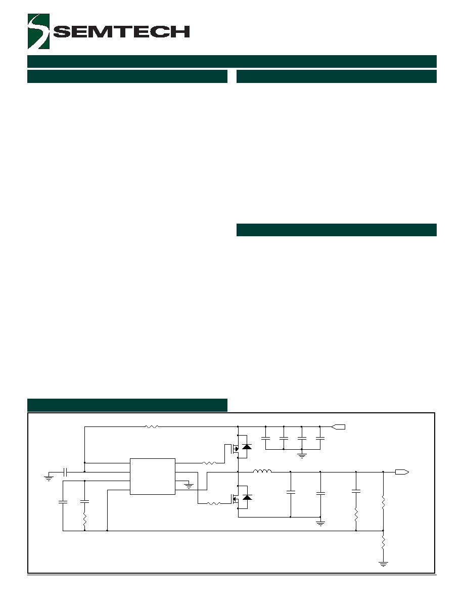
C2
6.8n
R1
5.11k
C7
150u
C1
470p
R6
1.0
R5
1.0
L1
1.6u
C4
22u
M2
Vo = 1.5V (as low as 0.8V )/6A
C10
22u
C11
22u
C12
22u
C13
22u
C9
3.3n
R8
169
R7
4.64k
R9
5.36k
VCC
1
SYNC/SLEEP
2
COMP
3
VSENSE
4
PHASE
5
GND
6
NDRV
7
PDRV
8
U1
SC4602B
C3
4.7u
M1
R15
1
Vin = 2.75V ~ 5.5V
* External components can be modified to provide a V
OUT
as low as 0.8V.
2
2004 Semtech Corp.
www.semtech.com
SC4602
POWER MANAGEMENT
Absolute Maximum Ratings
Electrical Characteristics
All voltages with respect to GND. Currents are positive into, negative out of the specified terminal.
Unless otherwise specified, V
CC
= 3.3V, T
A
= -40
C to 85
∞
C, T
A
= T
J.
Exceeding the specifications below may result in permanent damage to the device, or device malfunction. Operation outside of the parameters specified
in the Electrical Characteristics section is not implied.
r
e
t
e
m
a
r
a
P
l
o
b
m
y
S
m
u
m
i
x
a
M
s
t
i
n
U
V
(
e
g
a
tl
o
V
y
l
p
p
u
S
C
C
)
7
V
s
u
o
u
n
it
n
o
C
s
t
n
e
r
r
u
C
)
V
R
D
N
,
V
R
D
P
(
s
r
e
v
ir
D
t
u
p
t
u
O
5
2
.
0
±
A
)
T
E
S
I
,
S
F
,
P
E
E
L
S
/
C
N
Y
S
,
P
M
O
C
,
E
S
N
E
S
V
(
s
t
u
p
n
I
7
o
t
3
.
0
-
V
e
s
a
h
P
7
o
t
3
.
0
-
V
s
n
0
5
<
e
s
l
u
p
t
e
s
l
u
P
e
s
a
h
P
7
o
t
2
-
V
e
g
n
a
R
e
r
u
t
a
r
e
p
m
e
T
t
n
e
i
b
m
A
g
n
it
a
r
e
p
O
T
A
5
8
+
o
t
0
4
-
C
∞
e
g
n
a
R
e
r
u
t
a
r
e
p
m
e
T
e
g
a
r
o
t
S
T
G
T
S
0
5
1
+
o
t
5
6
-
C
∞
e
g
n
a
R
e
r
u
t
a
r
e
p
m
e
T
n
o
it
c
n
u
J
T
J
0
5
1
+
o
t
5
5
-
C
∞
e
s
a
C
o
t
n
o
it
c
n
u
J
e
c
n
a
d
e
p
m
I
l
a
m
r
e
h
T
C
J
9
.
1
4
W
/
C
∞
t
n
e
i
b
m
A
o
t
n
o
it
c
n
u
J
e
c
n
a
d
e
p
m
I
l
a
m
r
e
h
T
A
J
1
.
3
1
1
W
/
C
∞
.
c
e
S
0
1
)
g
n
ir
e
d
l
o
S
(
e
r
u
t
a
r
e
p
m
e
T
d
a
e
L
T
D
A
E
L
0
0
3
+
C
∞
)l
e
d
o
M
y
d
o
B
n
a
m
u
H
(
g
n
it
a
R
D
S
E
D
S
E
2
V
k
r
e
t
e
m
a
r
a
P
s
n
o
i
t
i
d
n
o
C
t
s
e
T
n
i
M
p
y
T
x
a
M
t
i
n
U
ll
a
r
e
v
O
e
g
a
tl
o
V
y
l
p
p
u
S
5
7
.
2
5
.
5
V
p
e
e
l
S
,t
n
e
r
r
u
C
y
l
p
p
u
S
V
P
E
E
L
S
/
C
N
Y
S
V
0
=
0
1
5
1
A
µ
g
n
it
a
r
e
p
O
,t
n
e
r
r
u
C
y
l
p
p
u
S
5
.
1
3
A
m
d
l
o
h
s
e
r
h
T
n
o
-
n
r
u
T
C
C
V
5
5
.
2
5
7
.
2
V
s
i
s
e
r
e
t
s
y
H
ff
o
-
n
r
u
T
C
C
V
0
5
1
V
m
r
e
i
f
il
p
m
A
r
o
r
r
E
e
c
n
e
r
e
f
e
R
l
a
n
r
e
t
n
I
T
A
C
∞
5
2
=
2
9
7
.
0
8
.
0
8
0
8
.
0
V
V
C
C
T
,
V
5
.
5
o
t
V
5
7
.
2
=
A
C
∞
5
2
=
8
8
7
.
0
8
.
0
2
1
8
.
0
e
r
u
t
a
r
e
p
m
e
T
4
8
7
.
0
8
.
0
6
1
8
.
0
t
n
e
r
r
u
C
s
a
i
B
E
S
N
E
S
V
5
2
A
n
n
i
a
G
p
o
o
L
n
e
p
O
)
1
(
V
P
M
O
C
V
8
.
1
o
t
V
4
.
0
=
0
7
0
8
B
d
h
t
d
i
w
d
n
a
B
n
i
a
G
y
ti
n
U
)
1
(
4
z
H
M
e
t
a
R
w
e
l
S
)
1
(
2
s
µ
/
V

3
2004 Semtech Corp.
www.semtech.com
SC4602
POWER MANAGEMENT
Electrical Characteristics (Cont.)
Unless otherwise specified, V
CC
= 3.3V, T
A
= -40
C to 85
∞
C, T
A
= T
J.
r
e
t
e
m
a
r
a
P
s
n
o
i
t
i
d
n
o
C
t
s
e
T
n
i
M
p
y
T
x
a
M
t
i
n
U
)
.
t
n
o
C
(
r
e
i
f
il
p
m
A
r
o
r
r
E
h
g
i
H
P
M
O
C
V
I
P
M
O
C
A
m
2
-
=
8
.
2
1
.
3
V
w
o
L
P
M
O
C
V
I
P
M
O
C
A
m
2
=
5
1
.
0
3
.
0
V
r
o
t
a
ll
i
c
s
O
)
A
2
0
6
4
C
S
(
y
c
a
r
u
c
c
A
l
a
it
i
n
I
T
A
H
G
I
H
=
C
N
Y
S
V
,
C
∞
5
2
=
0
6
2
0
0
3
0
4
3
z
H
k
)
B
2
0
6
4
C
S
(
y
c
a
r
u
c
c
A
l
a
it
i
n
I
T
A
H
G
I
H
=
C
N
Y
S
V
,
C
∞
5
2
=
0
8
4
0
5
5
0
2
6
z
H
k
d
l
o
h
s
e
r
h
T
w
o
L
P
E
E
L
S
/
C
N
Y
S
8
.
0
V
d
l
o
h
s
e
r
h
T
h
g
i
H
P
E
E
L
S
/
C
N
Y
S
0
.
2
V
y
e
ll
a
V
o
t
k
a
e
P
p
m
a
R
)
1
(
3
.
1
5
.
1
7
.
1
V
e
g
a
tl
o
V
k
a
e
P
p
m
a
R
)
1
(
5
8
.
1
9
.
1
V
e
g
a
tl
o
V
y
e
ll
a
V
p
m
a
R
)
1
(
3
.
0
5
3
.
0
V
t
i
m
i
L
t
n
e
r
r
u
C
,
t
r
a
t
S
t
f
o
S
,
p
e
e
l
S
t
n
e
r
r
u
C
s
a
i
B
t
u
p
n
I
p
e
e
l
S
V
0
=
P
E
E
L
S
/
C
N
Y
S
V
1
-
A
µ
e
m
i
T
t
r
a
t
S
tf
o
S
)
1
(
A
2
0
6
4
C
S
4
.
2
s
m
B
2
0
6
4
C
S
2
.
1
d
l
o
h
s
e
r
h
T
ti
m
i
L
t
n
e
r
r
u
C
)
2
(
V
o
t
e
c
n
e
r
e
f
e
R
C
C
T
,
J
C
∞
5
2
=
0
0
3
-
V
m
t
n
e
i
c
if
f
e
o
c
e
r
u
t
a
r
e
p
m
e
T
4
.
0
C
∞
/
%
e
m
i
T
k
n
a
l
B
ti
m
i
L
t
n
e
r
r
u
C
)
1
(
0
5
1
s
n
s
t
u
p
t
u
O
r
e
v
i
r
D
l
e
n
n
a
h
C
-
P
d
n
a
l
e
n
n
a
h
C
-
N
)
V
R
D
P
(
e
c
n
a
t
s
i
s
e
R
p
U
ll
u
P
)
2
(
I
,
V
3
.
3
=
c
c
V
T
U
O
)
e
c
r
u
o
s
(
A
m
0
0
1
-
=
3
s
m
h
o
)
V
R
D
P
(
e
c
n
a
t
s
i
s
e
R
n
w
o
D
ll
u
P
)
2
(
I
,
V
3
.
3
=
c
c
V
T
U
O
)
k
n
i
s
(
A
m
0
5
=
3
s
m
h
o
)
V
R
D
N
(
e
c
n
a
t
s
i
s
e
R
p
U
ll
u
P
)
2
(
I
,
V
3
.
3
=
c
c
V
T
U
O
)
e
c
r
u
o
s
(
A
m
0
0
1
-
=
3
s
m
h
o
)
V
R
D
N
(
e
c
n
a
t
s
i
s
e
R
n
w
o
D
ll
u
P
)
2
(
I
,
V
3
.
3
=
c
c
V
T
U
O
)
k
n
i
s
(
A
m
0
0
1
=
3
s
m
h
o
e
m
i
T
e
s
i
R
t
u
p
t
u
O
V
R
D
P
)
1
(
C
,
V
3
.
3
=
s
g
V
T
U
O
F
n
0
.
1
=
9
s
n
e
m
i
T
ll
a
F
t
u
p
t
u
O
V
R
D
P
)
1
(
C
,
V
3
.
3
=
s
g
V
T
U
O
F
n
0
.
1
=
2
1
s
n
4
2004 Semtech Corp.
www.semtech.com
SC4602
POWER MANAGEMENT
Notes:
(1) Guaranteed by design.
(2) Guaranteed by characterization.
(3) Dead time delay from PDRV high to NDRV high is adaptive. As the phase node voltage drops below 600mV due to PDRV
high, NDRV will start to turn high.
Electrical Characteristics (Cont.)
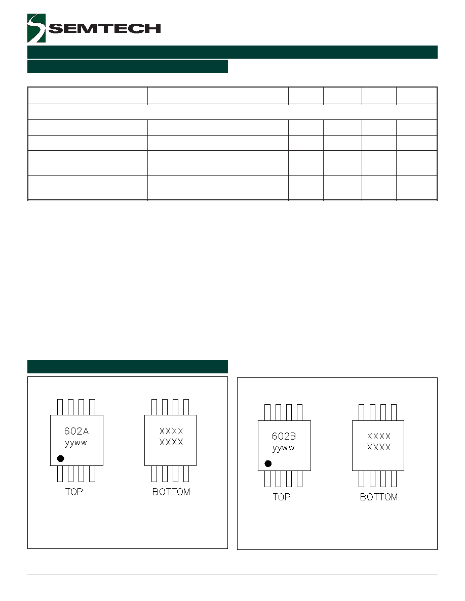
yyww = Date Code (Example: 0012)
xxxxxxxx = Semtech Lot No. (Example: E901
01-1)
Marking Information
yyww = Date Code (Example: 0012)
xxxxxxxx = Semtech Lot No. (Example: E901
01-1)
Unless otherwise specified, V
CC
= 3.3V, T
A
= -40
C to 85
∞
C, T
A
= T
J.
r
e
t
e
m
a
r
a
P
s
n
o
i
t
i
d
n
o
C
t
s
e
T
n
i
M
p
y
T
x
a
M
t
i
n
U
)
.
t
n
o
C
(
s
t
u
p
t
u
O
r
e
v
i
r
D
l
e
n
n
a
h
C
-
P
d
n
a
l
e
n
n
a
h
c
-
N
e
m
i
T
e
s
i
R
t
u
p
t
u
O
V
R
D
N
)
1
(
C
,
V
3
.
3
=
s
g
V
T
U
O
F
n
0
.
1
=
5
1
s
n
e
m
i
T
ll
a
F
t
u
p
t
u
O
V
R
D
N
)
1
(
C
,
V
3
.
3
=
s
g
V
T
U
O
F
n
0
.
1
=
5
1
s
n
y
a
l
e
D
e
m
it
d
a
e
D
)
h
g
i
h
V
R
D
N
o
t
h
g
i
h
V
R
D
P
(
)
1
(
e
v
it
p
a
d
a
y
a
l
e
D
e
m
it
d
a
e
D
)
w
o
l
V
R
D
P
o
t
w
o
l
V
R
D
N
(
)
1
(
0
5
s
n
5
2004 Semtech Corp.
www.semtech.com
SC4602
POWER MANAGEMENT
Ordering Information
Pin Descriptions
r
e
b
m
u
N
t
r
a
P
)
1
(
z
H
k
e
c
i
v
e
D
R
T
S
M
I
A
2
0
6
4
C
S
0
0
3
8
-
P
O
S
M
T
R
T
S
M
I
A
2
0
6
4
C
S
)
2
(
R
T
S
M
I
B
2
0
6
4
C
S
0
5
5
8
-
P
O
S
M
T
R
T
S
M
I
B
2
0
6
4
C
S
)
2
(
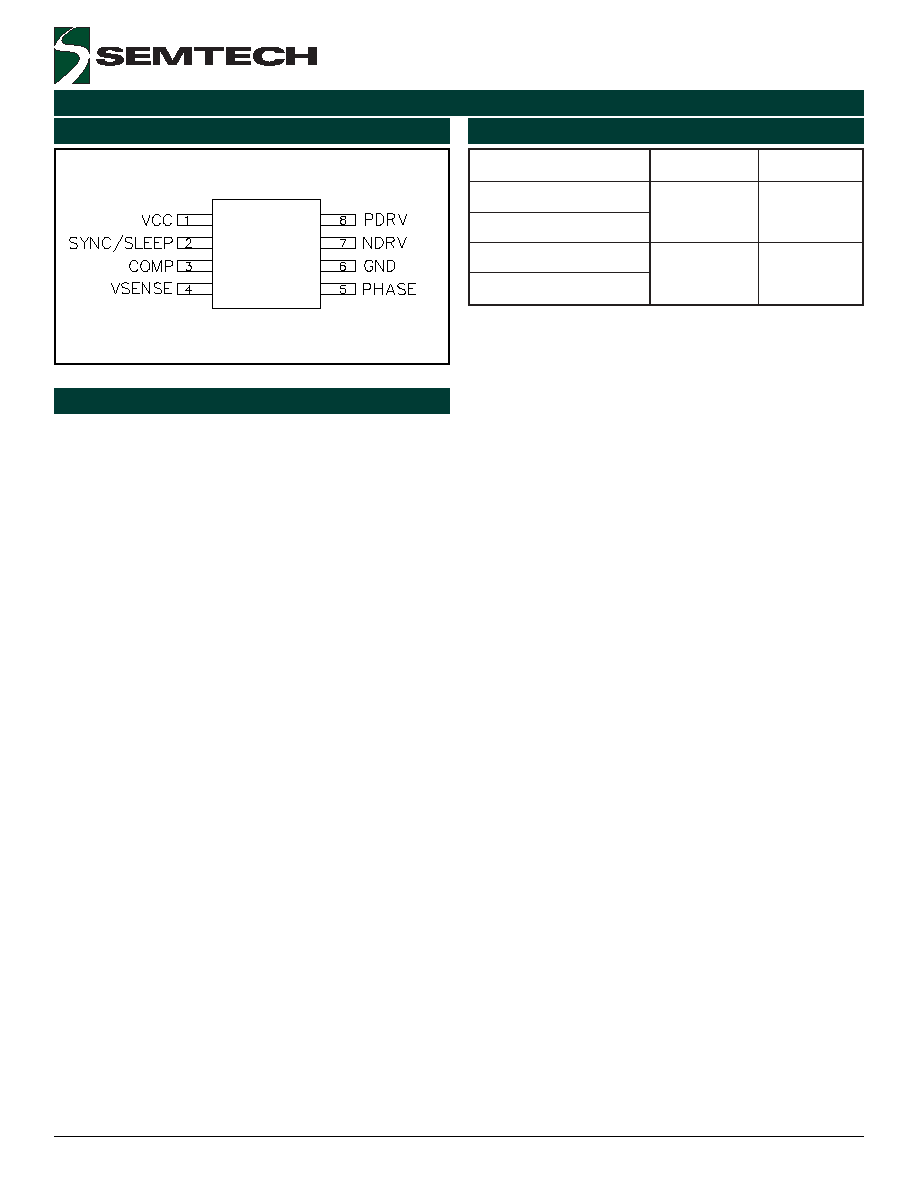
VCC: Positive supply rail for the IC. Bypass this pin to
GND with a 0.1 to 4.7µF low ESL/ESR ceramic capaci-
tor.
GND: All voltages are measured with respect to this pin.
All bypass and timing capacitors connected to GND should
have leads as short and direct as possible.
SYNC/SLEEP: The oscillator of SC4602A and SC4602B
are set to 300kHz and 550kHz respectively when SYNC/
SLEEP is pulled and held above 2V. Synchronous mode
operation is activated as the SYNC/SLEEP is driven by an
external clock. The oscillator and PWM are designed to
provide practical operation to 450kHz for SC4602A and
to 700kHz for SC4602B when synchronized. Sleep mode
is invoked if SYNC/SLEEP is pulled and held below 0.8V
which can be accomplished by an external gate or tran-
sistor. Sleepmode supply current is 10µA typical.
VSENSE: This pin is the inverting input of the voltage
amplifier and serves as the output voltage feedback point
for the Buck converter. It senses the output voltage through
an external divider.
COMP: This is the output of the voltage amplifier. The
voltage at this output is inverted internally and connected
to the non-inverting input of the PWM comparator. A lead-
lag network around the voltage amplifier compensates for
the two pole LC filter characteristic inherent to voltage mode
control and is required in order to optimize the dynamic
performance of the voltage mode control loop.
PHASE: This input is connected to the junction between
the two external power MOSFET transistors. The voltage
drop across the upper P-channel device is monitored by
PHASE during conduction and forms the current limit
comparator. Logic sets the PWM latch and terminates
the output pulse. The controller stops switching and goes
through a soft start sequence once the converter out-
put voltage drops below 68.75% its nominal voltage. This
prevents excess power dissipation in the PMOSFET dur-
ing a short circuit. The reverse current comparator senses
the drop across the lower N-channel MOSFET during its
conduction and disables the drive signal if a small posi-
tive voltage is present. To disable the overcurrent com-
parator, connect PHASE to VCC.
PDRV, NDRV: The PWM circuitry provides complemen-
tary drive signals to the output stages. Cross conduc-
tion of the external MOSFETS is prevented by monitoring
the voltage on the P-channel and N-channel driver pins
in conjunction with a time delay optimized for FET turn-
off characteristics.
(8 Pin MSOP)
Notes:
(1) Only available in tape and reel packaging. A reel
contains 2500 devices.
(2) Lead free product. This product is fully WEEE and
RoHS compliant.
Pin Configuration
Top View
6
2004 Semtech Corp.
www.semtech.com
SC4602
POWER MANAGEMENT
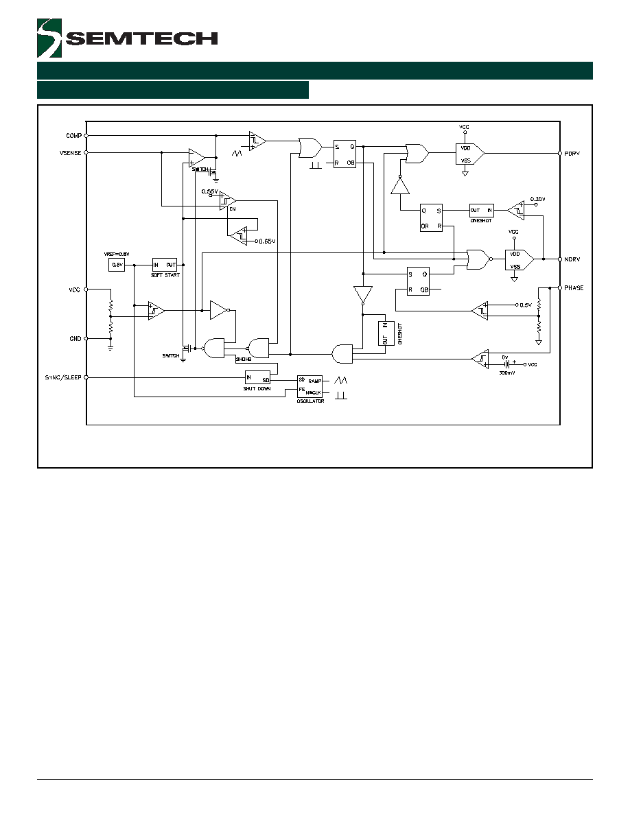
Block Diagram
7
2004 Semtech Corp.
www.semtech.com
SC4602
POWER MANAGEMENT
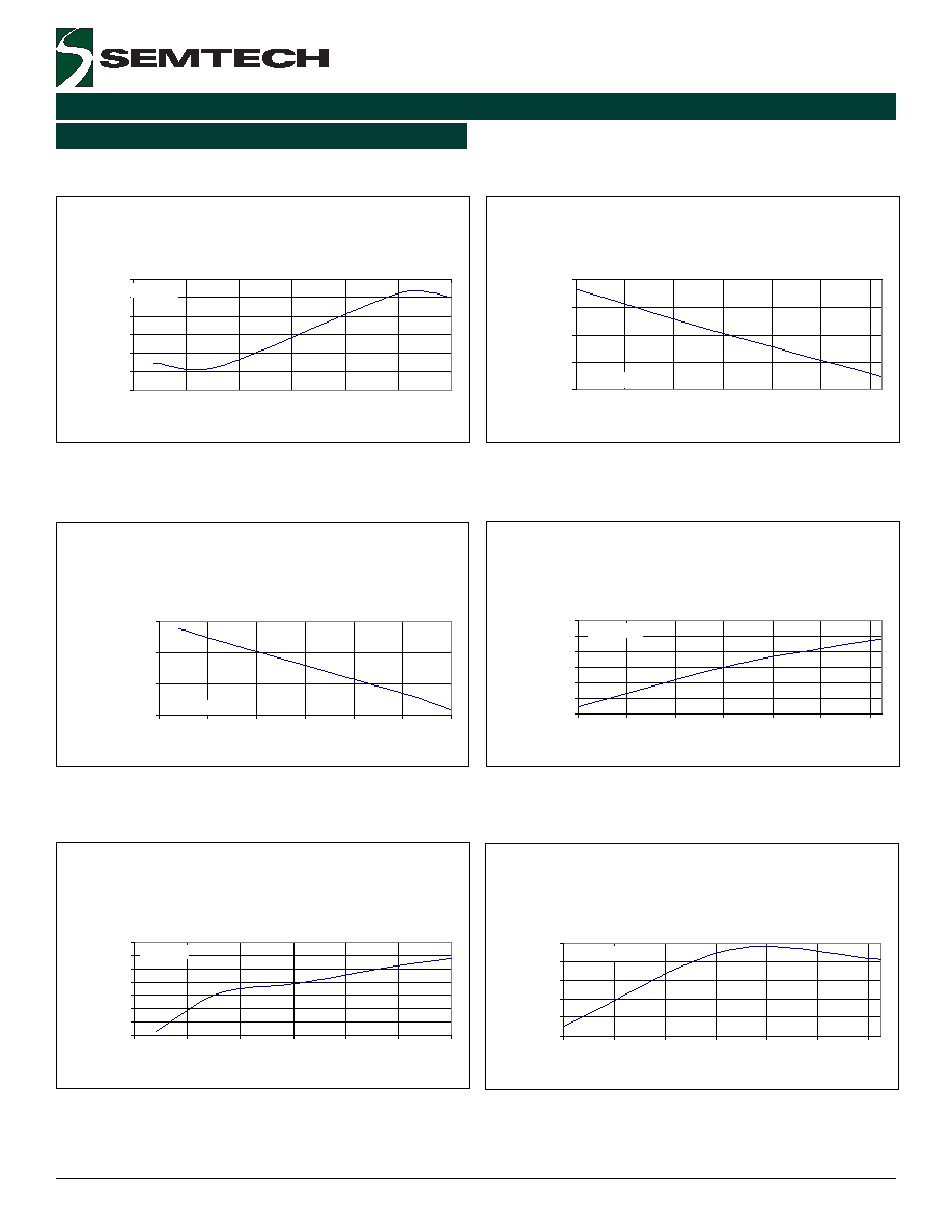
Typical Characteristic (Cont.)
Current Limit Threshold Voltage
vs
Input Voltage
-310.00
-305.00
-300.00
-295.00
-290.00
-285.00
-280.00
2.5
3
3.5
4
4.5
5
5.5
Vcc (V)
C
u
r
r
e
n
t
Li
m
i
t
Thr
e
s
ho
l
d
V
o
l
t
ag
e (
m
V
)
T
A
= 25∞C
Current Limit Threshold Voltage
vs
Temperature
-400.00
-350.00
-300.00
-250.00
-200.00
-40
-20
0
20
40
60
80
Temperature (∞C)
C
u
r
r
e
nt
Li
m
i
t
Thr
e
s
hol
d
V
o
l
t
ag
e (
m
V
)
Vcc = 3.3V
Sc4602A
Oscillator Internal Accuracy
vs
Input Voltage
275.000
280.000
285.000
290.000
2.5
3
3.5
4
4.5
5
5.5
Vcc (V)
I
n
t
e
rn
a
l
A
c
c
u
ra
cy
(k
H
z
)
TA = 25∞C
Sc4602A
Oscillator Internal Accuracy
vs
Temperature
270.000
275.000
280.000
285.000
290.000
295.000
300.000
-40
-20
0
20
40
60
80
Temperature (∞C)
I
n
t
e
rn
a
l
A
c
c
u
ra
cy
(k
H
z
)
Vcc = 3.3V
Sc4602A
Sense Voltage
vs
Input Voltage
802.000
802.200
802.400
802.600
802.800
803.000
803.200
803.400
2.5
3
3.5
4
4.5
5
5.5
Vcc (V)
S
e
n
s
e
V
o
l
t
ag
e (
m
V
)
T
A
= 25∞C
Sc4602A
Sense Voltage
vs
Temperature
798.000
799.000
800.000
801.000
802.000
803.000
-40
-20
0
20
40
60
80
Temperature (∞C)
S
e
n
s
e
V
o
l
t
ag
e (
m
V
)
Vcc = 3.3V
8
2004 Semtech Corp.
www.semtech.com
SC4602
POWER MANAGEMENT
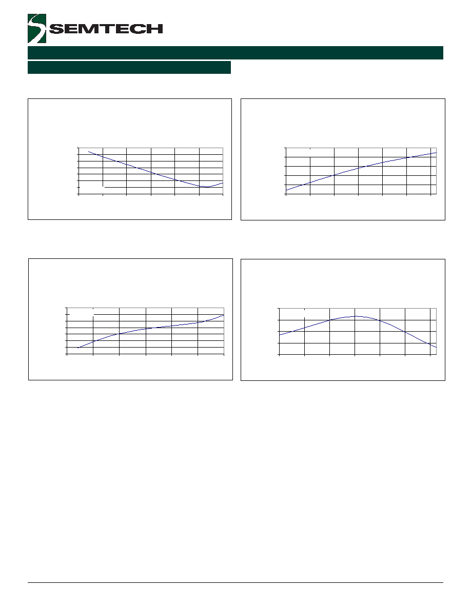
Typical Characteristic (Cont.)
Sc4602B
Oscillator Internal Accuracy
vs
Input Voltage
525.000
530.000
535.000
540.000
545.000
550.000
555.000
560.000
2.5
3
3.5
4
4.5
5
5.5
Vcc (V)
I
n
te
r
n
a
l
Ac
cu
r
a
cy
(k
H
z
)
TA = 25∞C
Sc4602B
Oscillator Internal Accuracy
vs
Temperature
520.000
530.000
540.000
550.000
560.000
570.000
-40
-20
0
20
40
60
80
Temperature (∞C)
I
n
te
r
n
a
l
Ac
cu
r
a
cy
(k
H
z
)
Vcc = 3.3V
Sc4602B
Sense Voltage
vs
Input Voltage
799.600
799.800
800.000
800.200
800.400
800.600
800.800
801.000
2.5
3
3.5
4
4.5
5
5.5
Vcc (V)
S
e
n
s
e
V
o
l
t
ag
e (
m
V
)
T
A
= 25∞C
Sc4602B
Sense Voltage
vs
Temperature
798.500
799.000
799.500
800.000
800.500
-40
-20
0
20
40
60
80
Temperature (∞C)
S
e
n
s
e
V
o
l
t
ag
e (
m
V
)
Vcc = 3.3V

9
2004 Semtech Corp.
www.semtech.com
SC4602
POWER MANAGEMENT
Applications Information
Enable
Pulling and holding the SYNC/SLEEP pin below 0.8V ini-
tializes the SLEEP mode of the SC4602with its typical
SLEEP mode supply current of 10uA. During the SLEEP
mode, the high side and low side MOSFETs are turned
off and the internal soft start voltage is held low.
Oscillator
The SC4602 is a constant frequency, voltage mode, and
synchronous step down controller ideal for low voltage,
high efficiency, precisely regulated output DC/DC con-
verters. Its internal free running oscillator sets the PWM
frequency at 300kHz for the SC4602A and 550kHz for
the SC4602B without any external components to set
the frequency. A 100% maximum duty cycle allows the
SC4602 to operate as a low dropout regulator in the
event of a low battery condition. An external clock con-
nected to SYNC/SLEEP activates its synchronous mode
and the frequency of the clock can be up to 450kHz for
the SC4602A and 700kH for the SC4602B.
UVLO
When the SYNC/SLEEP pin is pulled and held above 2V,
the voltage on the Vcc pin determines the operation of
the SC4602. As Vcc increases during start up, the UVLO
block senses Vcc and keeps the high side and low side
MOSFETs off and the internal soft start voltage low until
Vcc reaches 2.75V. If no faults are present, the SC4602
will initiate a soft start when Vcc exceeds 2.75V. A hys-
teresis (150mV) in the UVLO comparator provides noise
immunity during its start up.
Soft Start
The soft start function is required for step down control-
lers to prevent excess inrush current through the DC bus
during start up. Generally this can be done by sourcing a
controlled current into a timing capacitor and then using
the voltage across this capacitor to slowly ramp up the
error amp reference. The closed loop creates narrow
width driver pulses while the output voltage is low and
allows these pulses to increase to their steady state duty
cycle as the output voltage reaches its regulated value.
With this, the inrush current from the input side is con-
trolled. The duration of the soft start in the SC4602 is
controlled by an internal timing circuit which is used dur-
ing start up and over current to set the hiccup time. The
soft start time can be calculated by:
s
START
_
SOFT
f
720
T
=
As can be seen here, the soft start time is switching fre-
quency dependant. For example, if f
s
= 300kHz, T
SOFT
_
START
= 720/300k = 2.4ms. But if f
s
= 600kHz, T
SOFT
_
START
=
720/600k = 1.2ms.
The SC4602 implements its soft start by ramping up the
error amplifier reference voltage providing a controlled
slew rate of the output voltage, then preventing over-
shoot and limiting inrush current during its start up.
Over Current Protection
Over current protection for the SC4602 is implemented
by detecting the voltage drop of the high side P-MOSFET
during conduction, also known as high side R
DS(ON)
detec-
tion. This loss-less detection eliminates the sense resis-
tor and its loss. The overall efficiency is improved, and
the number of components and cost of the converter
are reduced. R
DS(ON)
sensing is by default inaccurate and
is mainly used to protect the power supply during a fault
case. The over current trigger point will vary from unit to
unit as the R
DS(ON)
of P-MOSFET varies. Even for the same
unit, the over current trigger point will vary as the junc-
tion temperature of P-MOSFET varies. The SC4602 pro-
vides a built-in 300mV voltage source. The over current
trigger point can be determined based on the internal
300mV voltage source and the R
DS(ON)
of P-MOSFET as
follows:
)
ON
(
DS
trigger
R
mV
300
I
=
Kelvin sensing connections should be used at the drain
and source of P-MOSFET.
The R
DS(ON)
sensing used in the SC4602 has an addi-
tional feature that enhances the performance of the over
current protection. Because the R
DS(ON)
has a positive
temperature coefficient, the 300mV voltage source has
a positive coefficient of about 0.4%/C∞ providing first
order correction for current sensing vs temperature. This
compensation depends on the high amount of thermal
transferring that typically exists between the high side P-
MOSFET and the SC4602 due to the compact layout of
the power supply.
10
2004 Semtech Corp.
www.semtech.com
SC4602
POWER MANAGEMENT
When the converter detects an over current condition (I
> I
MAX
) as shown in Figure 1, the first action the SC4602
takes is to enter cycle by cycle protection mode (Point B
to Point C), which responds to minor over current cases.
Then the output voltage is monitored. If the over current
and low output voltage (set at 68.75% of nominal out-
put voltage) occur at the same time, the Hiccup mode
operation (Point C to Point D) of the SC4602 is invoked
and the internal soft start capacitor is discharged. This is
like a typical soft start cycle.
I
MA
nom
O
V
-
6875
.
0
nom
O
V
-
O
V
O
I
A
B
D
C
nom
O
V
-
125
.
0
Figure 1. Over current protection characteristic of
SC4602
Power MOSFET Drivers
The SC4602 has two drivers for external complemen-
tary power MOSFETs. The driver block consists of one
high side P-MOSFET, 4
driver, PDRV, and one low side
5
, N-MOSFET driver, NDRV, which are optimized for driv-
ing external power MOSFETs in a synchronous buck con-
verter. The output drivers also have gate drive non-over-
lap mechanism that gives a dead time between PDRV
and NDRV transitions to avoid potential shoot through
problems in the external MOSFETs. By using the proper
design and the appropriate MOSFETs, a 6A converter can
be achieved. As shown in Figure 2, t
d1,
the delay from
the P-MOSFET off to the N-MOSFET on is adaptive by
detecting the voltage of the phase node. t
d2
, the delay
from the N-MOSFET off to the P-MOSFET on is fixed, is
100ns for the SC4602. This control scheme guarantees
avoiding the cross conduction or shoot through between
Applications Information (Cont.)
two MOSFETs and minimizes the conduction loss in the
bottom diode for high efficiency applications.
NMOSFET Gate Drive
PMOSFET Gate Drive
Phase node
Ground
t
d1
t
d2
Figure 2. Timing Waveforms for Gate Drives and Phase
Node
Inductor Selection
The factors for selecting the inductor include its cost,
efficiency, size and EMI. For a typical SC4602 applica-
tion, the inductor selection is mainly based on its value,
saturation current and DC resistance. Increasing the in-
ductor value will decrease the ripple level of the output
voltage while the output transient response will be de-
graded. Low value inductors offer small size and fast tran-
sient responses while they cause large ripple currents,
poor efficiencies and more output capacitance to smooth
out the large ripple currents. The inductor should be able
to handle the peak current without saturating and its
copper resistance in the winding should be as low as
possible to minimize its resistive power loss. A good trade-
off among its size, loss and cost is to set the inductor
ripple current to be within 15% to 30% of the maximum
output current.
The inductor value can be determined according to its
operating point and the switching frequency as follows:
OMAX
s
I
O
I
O
I
I
f
V
)
V
V
(
V
L
-
=
Where:
f
s
= switching frequency and
I = ratio of the peak to peak inductor current to the
maximum output load current.
The peak to peak inductor current is:
OMAX
P
P
I
I
I
∑
=
-
11
2004 Semtech Corp.
www.semtech.com
SC4602
POWER MANAGEMENT
After the required inductor value is selected, the proper
selection of the core material is based on the peak in-
ductor current and efficiency requirements. The core
must be able to handle the peak inductor current I
PEAK
without saturation and produce low core loss during the
high frequency operation.
2
I
I
I
p
p
OMAX
PEAK
-
+
=
The power loss for the inductor includes its core loss and
copper loss. If possible, the winding resistance should
be minimized to reduce inductor's copper loss. The core
loss can be found in the manufacturer's datasheet. The
inductor' copper loss can be estimated as follows:
WINDING
LRMS
2
COPPER
R
I
P
=
Where:
I
LRMS
is the RMS current in the inductor. This current can
be calculated as follows:
2
OMAX
LRMS
I
3
1
1
I
I
+
=
Output Capacitor Selection
Basically there are two major factors to consider in se-
lecting the type and quantity of the output capacitors.
The first one is the required ESR (Equivalent Series Re-
sistance) which should be low enough to reduce the volt-
age deviation from its nominal one during its load changes.
The second one is the required capacitance, which should
be high enough to hold up the output voltage. Before the
SC4602 regulates the inductor current to a new value
during a load transient, the output capacitor delivers all
the additional current needed by the load. The ESR and
ESL of the output capacitor, the loop parasitic inductance
between the output capacitor and the load combined
with inductor ripple current are all major contributors to
the output voltage ripple. Surface mount speciality poly-
mer aluminum electrolytic chip capacitors in UE series
from Panasonic provide low ESR and reduce the total
capacitance required for a fast transient response.
POSCAP from Sanyo is a solid electrolytic chip capacitor
which has a low ESR and good performance for high fre-
quency with a low profile and high capacitance. Above
mentioned capacitors are recommended to use in
SC4602 applications.
Input Capacitor Selection
The input capacitor selection is based on its ripple cur-
rent level, required capacitance and voltage rating. This
capacitor must be able to provide the ripple current by
the switching actions. For the continuous conduction
mode, the RMS value of the input capacitor can be cal-
culated from:
I
2
O
I
O
OMAX
)
RMS
(
CIN
V
)
V
V
(
V
I
I
-
=
This current gives the capacitor's power loss as follows:
)
ESR
(
CIN
)
RMS
(
CIN
2
CIN
R
I
P
=
This capacitor's RMS loss can be a significant part of the
total loss in the converter and reduce the overall con-
verter efficiency. The input ripple voltage mainly depends
on the input capacitor's ESR and its capacitance for a
given load, input voltage and output voltage. Assuming
that the input current of the converter is constant, the
required input capacitance for a given voltage ripple can
be calculated by:
)
R
I
V
(
fs
)
D
1
(
D
I
C
)
ESR
(
CIN
OMAX
I
OMAX
IN
-
-
=
Where:
D = V
O
/V
I
, duty ratio and
DV
I
= the given input voltage ripple.
Because the input capacitor is exposed to the large surge
current, attention is needed for the input capacitor. If
tantalum capacitors are used at the input side of the
converter, one needs to ensure that the RMS and surge
ratings are not exceeded. For generic tantalum capaci-
tors, it is wise to derate their voltage ratings at a ratio of
2 to protect these input capacitors.
Power Mosfet Selection
The SC4602 can drive a P-MOSFET at the high side and
an N-MOSFET synchronous rectifier at the low side. The
use of the high side P-MOSFET eliminates the need for
an external charge pump and simplifies the high side gate
driver circuit.
Applications Information (Cont.)
12
2004 Semtech Corp.
www.semtech.com
SC4602
POWER MANAGEMENT
For the top MOSFET, its total power loss includes its con-
duction loss, switching loss, gate charge loss, output ca-
pacitance loss and the loss related to the reverse recov-
ery of the bottom diode, shown as follows:
s
I
rr
OSS
s
GATE
GT
2
GS
GD
G
GATE
s
I
PEAK
_
TOP
ON
_
TOP
RMS
_
TOP
2
TOTAL
_
TOP
f
V
)
Q
Q
(
f
V
Q
)
Q
Q
(
R
V
f
V
I
R
I
P
+
+
+
+
+
=
Where:
R
G
= gate drive resistor,
Q
GD
= the gate to drain charge of the top MOSFET,
Q
GS2
= the gate to source charge of the top MOSFET,
Q
GT
= the total gate charge of the top MOSFET,
Q
OSS
= the output charge of the top MOSFET and
Q
rr
= the reverse recovery charge of the bottom diode.
For the top MOSFET, it experiences high current and high
voltage overlap during each on/off transition. But for the
bottom MOSFET, its switching voltage is the bottom
diode's forward drop during its on/off transition. So the
switching loss for the bottom MOSFET is negligible. Its
total power loss can be determined by:
F
AVG
D
s
GATE
GB
ON
_
BOT
RMS
_
BOT
2
TOTAL
_
BOT
V
_
I
f
V
Q
R
I
P
+
+
=
Where:
Q
GB
= the total gate charge of the bottom MOSFET and
V
F
= the forward voltage drop of the bottom diode.
For a low voltage and high output current application such
as the
3.3V/1.5V@6A
case, the conduction loss is often
dominant and selecting low R
DS(ON)
MOSFETs will notice-
ably improve the efficiency of the converter even though
they give higher switching losses.
The gate charge loss portion of the top/bottom MOSFET's
total power loss is derived from the SC4602. This gate
charge loss is based on certain operating conditions (f
s
,
V
GATE
, and I
O
).
The thermal estimations have to be done for both
MOSFETs to make sure that their junction temperatures
do not exceed their thermal ratings according to their
total power losses P
TOTAL
, ambient temperature T
a
and their
thermal resistances R
ja
as follows:
ja
TOTAL
a
(max)
j
R
P
T
T
+
<
Applications Information (Cont.)
Loop Compensation Design
For a DC/DC converter, it is usually required that the
converter has a loop gain of a high cross-over frequency
for fast load response, high DC and low frequency gain
for low steady state error, and enough phase margin for
its operating stability. Often one can not have all these
properties at the same time. The purpose of the loop
compensation is to arrange the poles and zeros of the
compensation network to meet the requirements for a
specific application.
The SC4602 has an internal error amplifier and requires
the compensation network to connect among the COMP
pin and VSENSE pin, GND, and the output as shown in
Figure 3. The compensation network includes C1, C2,
R1, R7, R8 and C9.
R9 is used to program the output voltage according to:
)
R
R
1
(
8
.
0
V
9
7
O
+
=
C2
R1
C1
Vo
L1
C4
C9
R8
R7
R9
SC4602
VCC
SYNC/SLEEP
COMP
VSENSE
PHASE
GND
NDRV
PDRV
Figure 3. Compensation network provides 3
poles and 2 zeros.
For voltage mode step down applications as shown in
Figure 3, the power stage transfer function is:
4
1
2
1
4
C
I
VD
C
L
s
R
L
s
1
C
R
1
s
1
V
)
s
(
G
+
+
+
=
13
2004 Semtech Corp.
www.semtech.com
SC4602
POWER MANAGEMENT
Applications Information (Cont.)
Where:
R = load resistance and
R
C
= C
4
's ESR.
The compensation network will have the characteristic
as follows:
2
P
2
Z
1
P
1
Z
I
COMP
s
1
s
1
s
1
s
1
s
)
s
(
G
+
+
+
+
=
Where:
)
C
C
(
R
1
2
1
7
I
+
=
2
1
1
Z
C
R
1
=
9
8
7
2
Z
C
)
R
R
(
1
+
=
2
1
1
2
1
1
P
C
C
R
C
C
+
=
9
8
2
P
C
R
1
=
After the compensation, the converter will have the fol-
lowing loop gain:
4
1
2
1
4
C
2
P
2
Z
1
P
1
Z
I
I
M
VD
COMP
PWM
C
L
s
R
L
s
1
C
R
1
s
1
s
1
s
1
s
1
s
1
s
V
V
1
)
s
(
G
)
s
(
G
G
)
s
(
T
+
+
+
+
+
+
+
=
=
Where:
G
PWM
= PWM gain and
V
M
= 1.5V, ramp peak to valley voltage of SC4602.
The design guidelines for the SC4602 applications are
as following:
1. Set the loop gain crossover corner frequency
C
for
given switching corner frequency
S
=2pf
s
,
2. Place an integrator at the origin to increase DC and
low frequency gains,
3. Select
Z1
and
Z2
such that they are placed near
O
to damp the peaking and the loop gain has a
-20dB/dec rate to go across the 0dB line for
obtaining a wide bandwidth,
4. Cancel the zero from C
4
's ESR by a compensator
pole
P1
(
P1
=
ESR
= 1/( R
C
C
4
)),
5. Place a high frequency compensator pole
p
2
(
p
2
= pf
s
) to get the maximum attenuation of the
switching
ripple and high frequency noise with the adequate
phase lag at
C
.
The compensated loop gain will be as given in Figure 4:
-20dB/dec
0dB
Gd
T
Z1
Z2
p1
p2
c
ESR
o
Loop gain T(s)
Power stage G
VD
(s)
-40dB/dec
Figure 4. Asymptotic diagrams of power stage and its
loop gain
14
2004 Semtech Corp.
www.semtech.com
SC4602
POWER MANAGEMENT
Applications Information (Cont.)
Layout Guideline
In order to achieve optimal electrical, thermal and noise
performance for high frequency converters, special at-
tention must be paid to the PCB layouts. The goal of lay-
out optimization is to identify the high di/dt loops and
minimize them. The following guideline should be used to
ensure proper functions of the converters.
1. A ground plane is recommended to minimize noises
and copper losses, and maximize heat dissipation.
2. Start the PCB layout by placing the power compo-
nents first. Arrange the power circuit to achieve a
clean power flow route. Put all the connections on
one side of the PCB with wide copper filled areas if
possible.
3. The Vcc bypass capacitor should be placed next to
the Vcc and GND pins.
4. The trace connecting the feedback resistors to the
output should be short, direct and far away from the
noise sources such as the phase node and switching
components.
5. Minimize the traces between PDRV/NDRV and the
gates of the MOSFETs to reduce their impedance to
drive the MOSFETs.
6. Minimize the loop including input capacitors, top/bot-
tom MOSFETs. This loop passes high di/dt current.
Make sure the trace width is wide enough to reduce
copper losses in this loop.
7. The PHASE connection to P-MOSFET for current sens-
ing must use Kelvin connection.
8. Maximize the trace width of the loop connecting the
inductor, bottom MOSFET and the output capacitors.
9. Connect the ground of the feedback divider and the
compensation components directly to the GND pin
of the SC4602 by using a separate ground trace.
Then connect this pin to the ground of the output
capacitor as close as possible.
A Design Example: 3.3V to1.5V @6A application with SC4602B (NH020 footprint)
Figure 5. Schematic for
3.3V/1.5V@6A
with SC4602B application
R2
3.32K
C2
6.8n
R1
5.11k
C7
150u
C1
470p
R6
1.0
R5
1.0
L1
1.6u
C4
22u
M2
C10
22u
C11
22u
C12
22u
C13
22u
Vin = 3.3V
C9
3.3n
R8
169
R7
4.64k
R9
5.36k
R10
100
Vo = 1.5V/6A
U1
SC4602B
VCC
1
SY NC/SLEEP
2
COMP
3
VSENSE
4
PHASE
5
GND
6
NDRV
7
PDRV
8
J2
1
2
3
4
5
C3
4.7u
J1
1
2
3
4
5
6
GND
ON/OFF
TRIM
R11
100
ON/OFF
M1
R15
1

15
2004 Semtech Corp.
www.semtech.com
SC4602
POWER MANAGEMENT
Bill of Materials - 3.3V to 1.5V @ 6A
m
e
t
I
y
t
Q
e
c
n
e
r
e
f
e
R
e
u
l
a
V
r
e
r
u
t
c
a
f
u
n
a
M
/.
o
N
t
r
a
P
1
1
1
C
F
p
0
7
4
2
1
2
C
F
n
8
.
6
3
1
3
C
F
u
7
.
4
c
i
m
a
r
e
c
,
5
0
8
0
4
5
3
1
C
,
2
1
C
,
1
1
C
,
0
1
C
,
4
C
F
u
2
2
M
6
2
2
J
0
R
5
X
5
2
2
3
C
:
N
/
P
K
D
T
5
1
7
C
,
F
u
0
5
1
,r
o
ti
c
a
p
a
c
P
S
V
3
.
6
,
m
h
o
m
5
1
c
i
n
o
s
a
n
a
P
6
1
9
C
F
n
3
.
3
7
1
1
J
6
N
O
C
8
1
2
J
5
N
O
C
9
1
1
L
,r
o
t
c
u
d
n
i
r
e
w
o
p
T
M
S
3
.
3
,
A
2
.
2
1
,
%
0
3
-
/
+
H
u
6
.
1
x
a
m
m
h
o
m
:
N
/
P
.
c
i
n
o
s
a
n
a
P
S
6
R
1
F
6
P
Q
T
E
0
1
1
1
M
d
li
h
c
r
i
a
F
,
8
-
O
S
,
5
7
3
6
S
D
F
P
T
E
F
S
O
M
8
-
O
S
1
1
1
1
M
d
li
h
c
r
i
a
F
,
8
-
O
S
,
A
0
8
6
6
S
D
F
N
T
E
F
S
O
M
8
-
O
S
2
1
1
1
R
k
1
1
.
5
3
1
1
2
R
k
2
3
.
3
4
1
1
5
1
R
1
5
1
2
6
R
,
5
R
0
.
1
6
1
1
7
R
k
4
6
.
4
7
1
1
8
R
9
6
1
8
1
1
9
R
k
6
3
.
5
9
1
2
1
1
R
,
0
1
R
0
0
1
0
2
1
1
U
B
2
0
6
4
C
S
R
T
S
M
I
B
2
0
6
4
C
S
:
N
/
P
h
c
e
t
m
e
S
:
s
t
n
e
n
o
p
m
o
c
y
e
K
h
c
e
t
m
e
S
,
B
2
0
6
4
C
S
:
1
U
d
li
h
c
r
i
a
F
,
8
-
O
S
,
5
7
3
6
S
D
F
:
1
M
d
li
h
c
r
i
a
F
,
8
-
O
S
,
A
0
8
6
6
S
D
F
:
2
M
c
i
n
o
s
a
n
a
P
,
V
3
.
6
,
m
h
o
m
5
1
,
F
u
0
5
1
,r
o
ti
c
a
p
a
c
P
S
:
7
C
.
c
i
n
o
s
a
n
a
P
S
6
R
1
F
6
P
Q
T
E
.
x
a
m
n
h
o
m
3
.
3
,
A
2
.
2
1
,
%
0
3
-
/
+
H
u
6
.
1
,r
o
t
c
u
d
n
i
r
e
w
o
p
T
M
S
:
1
L
.
e
g
a
k
c
a
p
3
0
6
0
D
M
S
n
i
e
r
a
s
r
o
ti
c
a
p
a
c
d
n
a
s
r
o
t
s
i
s
e
r
ll
a
,
d
e
if
i
c
e
p
s
s
s
e
l
n
U
%
0
2
-
/
+
e
r
a
s
r
o
ti
c
a
p
a
c
ll
a
d
n
a
%
1
-
/
+
e
r
a
s
r
o
t
s
i
s
e
R
16
2004 Semtech Corp.
www.semtech.com
SC4602
POWER MANAGEMENT
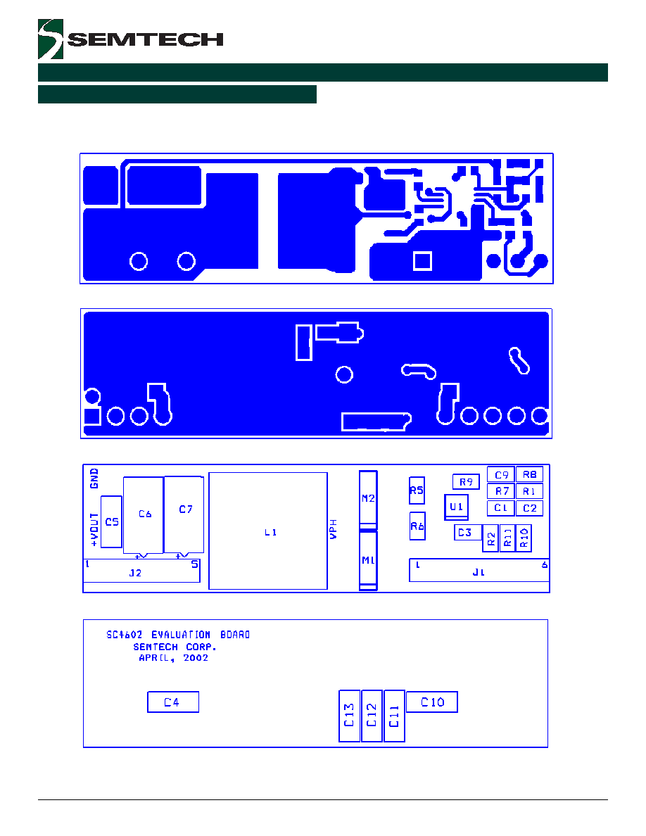
PCB Layout - 3.3V to 1.5V @ 6A
PCB layout information for
3.3V to1.5V @6A with SC4602B application (NH020 footprint)
Top
Bottom
Top
Bottom
17
2004 Semtech Corp.
www.semtech.com
SC4602
POWER MANAGEMENT
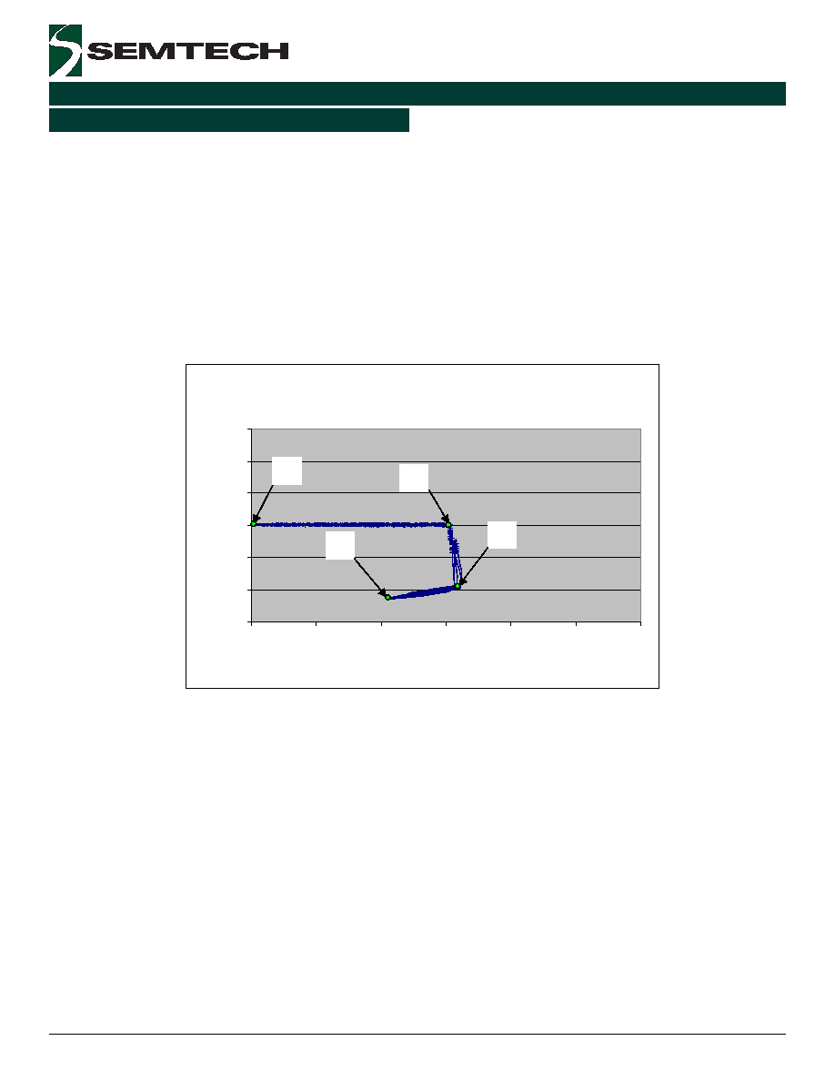
Typical Characteristic
Over current protection characteristic of SC4602B for 3.3V to1.5V @6A application:
The over current protection curve below is obtained by applying a gradually increased load while the load current
and the output voltage are monitored and measured. When the load current is increased from 0 to 9A (over current
trigger point), the output voltage is 1.5V, corresponding from Point A to Point B. As the load current increases
further from 9A to 9.6A, the output voltage drops significantly from 1.5V (Point B) to 0.54V (Point C). Because an
over current and a lower output voltage (0.54V<68.75%*1.5V=1.03V) are present at Point C, the SC4602B enters
its HICCUP mode. Then the locus of the output current and the output voltage follows Line CD as shown in the
curve. Due to the over current applied, the HICCUP protection will go back and forth on Line CD. This prevents
excess power dissipation in the P-MOSFET during a short output conditio
Overcurrent protection
0
0.5
1
1.5
2
2.5
3
0
3
6
9
12
15
18
Output Current (A)
O
u
t
put
V
o
l
t
a
g
e
(
V
)
B
C
D
A
18
2004 Semtech Corp.
www.semtech.com
SC4602
POWER MANAGEMENT
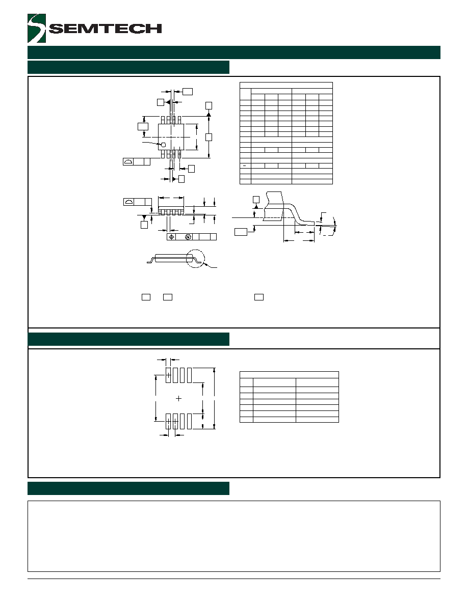
Outline Drawing - MSOP-8
Semtech Corporation
Power Management Products Division
200 Flynn Road, Camarillo, CA 93012
Phone: (805)498-2111 FAX (805)498-3804
Contact Information
Land Pattern - MSOP-8
0∞
.010
.004
-
.016
.003
.024
(.037)
-
.000
.030
-
-
-
-
0.25
0.10
8∞
0∞
-
8∞
0.60
(.95)
.032
.009
0.40
0.08
.043
.006
.037 0.75
0.00
-
0.80
0.23
-
0.95
1.10
0.15
-
-
-
3. DIMENSIONS "E1" AND "D" DO NOT INCLUDE MOLD FLASH, PROTRUSIONS
OR GATE BURRS.
-B-
CONTROLLING DIMENSIONS ARE IN MILLIMETERS (ANGLES IN DEGREES).
DATUMS AND TO BE DETERMINED AT DATUM PLANE
NOTES:
1.
2.
-A-
-H-
SIDE VIEW
A
B
C
e
H
e/2
D
PLANE
DETAIL
.193 BSC
.026 BSC
aaa C
SEATING
ccc C
2X N/2 TIPS
INDICATOR
E/2
PIN 1
2X
8
bbb
C A-B D
SEE DETAIL
A1
A
A2
bxN
D
0.25
A
PLANE
GAGE
.005
E1
1 2
N
.114
.114
.118
.118
.009
-
8
01
c
(L1)
L
A
0.13
3.00
3.00
4.90 BSC
0.65 BSC
.122
.122
2.90
2.90
.015 0.22
3.10
3.10
0.38
-
REFERENCE JEDEC STD MO-187, VARIATION AA.
4.
DIM
ccc
A1
e
bbb
aaa
01
L1
N
L
D
E1
E
A2
b
c
A
MILLIMETERS
NOM
DIMENSIONS
INCHES
MIN NOM MAX MIN
MAX
E
THIS LAND PATTERN IS FOR REFERENCE PURPOSES ONLY.
CONSULT YOUR MANUFACTURING GROUP TO ENSURE YOUR
COMPANY'S MANUFACTURING GUIDELINES ARE MET.
NOTES:
1.
P
X
(C)
Y
Z
G
.224
.063
.016
.026
(.161)
.098
(4.10)
5.70
1.60
0.40
0.65
2.50
MILLIMETERS
DIMENSIONS
DIM
INCHES
X
Z
Y
C
P
G