 | ÐлекÑÑоннÑй компоненÑ: SC4605 | СкаÑаÑÑ:  PDF PDF  ZIP ZIP |
SC4605 data sheet
1
www.semtech.com
SC4605
Low Input, High Efficiency
Synchronous, Step Down Controller
POWER MANAGEMENT
Revision: July 22, 2003
Description
Features
Applications
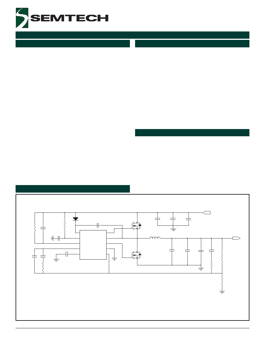
Typical Application Circuit
BICMOS voltage mode PWM controller
2.8V to 5.5V Input voltage range
Output voltages as low as 0.8V
+/-1% Reference accuracy
Sleep mode (Icc = 10µA typ)
Lossless adjustable short circuit current limiting
Combination pulse by pulse & hiccup mode
current limit
High efficiency synchronous switching
0% to 97% Duty cycle range
1A Peak current driver
10-Pin MSOP package
Distributed power architecture
Servers/workstations
Local microprocessor core power supplies
DSP and I/O power supplies
Battery powered applications
Telecommunications equipment
Data processing applications
The SC4605 is a voltage mode step down (buck) regula-
tor controller that provides accurate high efficiency power
conversion from a input supply range of 2.8V to 5.5V. A
high level of integration reduces external component
count, and makes it suitable for low voltage applications
where cost, size and efficiency are critical.
The SC4605 drives external N-channel MOSFETs with 1A
peak current. A non-overlap protection is provided for
the gate drive signals to prevent shoot through of the
MOSFET pair. The voltage drop across the high side
MOSFET during its conduction is sensed for lossless short
circuit current limiting.
The quiescent supply current in sleep mode is typically
lower than 10
µ
A. A 1.8ms soft start is internally provided
to prevent output voltage overshoot during start-up.
The SC4605 is an ideal choice for 3.3V, 5V or other low
input supply systems. It's available in 10 pin MSOP pack-
age.
*
External components can be modified to provide a Vout as low as 0.8V.
R3
C3
4.7u
C2 2.2n
C6
330u
R1
14.3k
C1
180p
C14
0.1u
Vin = 2.8V - 5.5V
D2
L1
1.8u
C5
22u
C4
22u
Vout = 1.5V (as low as 0.8V * ) / 12A
C71
1u
M1
C10
220u
M2
C12
22u
C9
4.7n
R8
200
R7
10k
R9
11.5k
C20
470pF
U1
SC4605
VCC
2
ISET
3
COMP
4
FSET
5
BST
1
DRVH
10
DRVL
8
VSENSE
6
GND
7
PHASE
9
C11
22u
R13
1
2
2003 Semtech Corp.
www.semtech.com
SC4605
POWER MANAGEMENT
Absolute Maximum Ratings
Electrical Characteristics
r
e
t
e
m
a
r
a
P
s
n
o
i
t
i
d
n
o
C
t
s
e
T
n
i
M
p
y
T
x
a
M
t
i
n
U
ll
a
r
e
v
O
e
g
a
tl
o
V
y
l
p
p
u
S
8
.
2
5
.
5
V
p
e
e
l
S
,t
n
e
r
r
u
C
y
l
p
p
u
S
V
0
=
C
N
Y
S
0
1
5
1
A
µ
s
a
i
B
,t
n
e
r
r
u
C
y
l
p
p
u
S
V
C
C
=
V
5
.
5
1
3
A
m
d
l
o
h
s
e
r
h
T
n
o
-
n
r
u
T
C
C
V
7
.
2
8
.
2
V
s
i
s
e
r
e
t
s
y
H
ff
o
-
n
r
u
T
C
C
V
5
2
1
V
m
r
e
i
f
il
p
m
A
r
o
r
r
E
e
g
a
tl
o
V
t
u
p
n
I
)
e
c
n
e
r
e
f
e
R
l
a
n
r
e
t
n
I
(
T
A
C
°
5
2
=
2
9
7
.
0
8
.
0
8
0
8
.
0
V
V
C
C
T
,
V
5
.
5
~
V
8
.
2
=
A
C
°
5
2
=
8
8
7
.
0
8
.
0
2
1
8
.
0
e
r
u
t
a
r
e
p
m
e
T
6
8
7
.
0
8
.
0
4
1
8
.
0
t
n
e
r
r
u
C
s
a
i
B
E
S
N
E
S
V
5
2
A
n
n
i
a
G
p
o
o
L
n
e
p
O
)
1
(
V
P
M
O
C
V
5
.
2
o
t
5
.
0
=
0
8
B
d
h
t
d
i
w
d
n
a
B
n
i
a
G
y
ti
n
U
)
1
(
4
z
H
M
e
t
a
R
w
e
l
S
)
1
(
2
s
µ
/
V
h
g
i
H
T
U
O
V
I
P
M
O
C
A
m
2
-
=
V
C
C
5
.
0
-
V
C
C
2
.
0
-
V
w
o
L
T
U
O
V
I
P
M
O
C
A
m
2
=
1
.
0
5
2
.
0
V
r
e
t
e
m
a
r
a
P
l
o
b
m
y
S
m
u
m
i
x
a
M
s
t
i
n
U
V
(
e
g
a
tl
o
V
y
l
p
p
u
S
C
C
)
7
V
s
t
n
e
r
r
u
C
)
L
V
R
D
,
H
V
R
D
(
s
r
e
v
ir
D
t
u
p
t
u
O
s
u
o
u
n
it
n
o
C
k
a
e
P
5
2
.
0
-
/
+
A
0
0
.
1
-
/
+
A
)
T
E
S
I
,
C
N
Y
S
/
S
F
,
P
M
O
C
,
E
S
N
E
S
V
(
s
t
u
p
n
I
7
o
t
3
.
0
-
V
E
S
A
H
P
5
.
5
o
t
3
.
0
-
V
s
n
0
0
1
<
e
s
l
u
p
t
e
s
l
u
P
E
S
A
H
P
7
o
t
2
-
V
e
g
n
a
R
e
r
u
t
a
r
e
p
m
e
T
t
n
e
i
b
m
A
g
n
it
a
r
e
p
O
T
A
5
8
+
o
t
0
4
-
C
°
e
g
n
a
R
e
r
u
t
a
r
e
p
m
e
T
e
g
a
r
o
t
S
T
G
T
S
0
5
1
+
o
t
5
6
-
C
°
e
g
n
a
R
e
r
u
t
a
r
e
p
m
e
T
n
o
it
c
n
u
J
T
J
0
5
1
+
o
t
5
5
-
C
°
.
c
e
S
0
1
)
g
n
ir
e
d
l
o
S
(
e
r
u
t
a
r
e
p
m
e
T
d
a
e
L
T
D
A
E
L
0
0
3
+
C
°
All voltages with respect to GND. Currents are positive into, negative out of the specified terminal.
Unless otherwise specified, VCC = 5V, CT = 470pF, T
A
= -40°C to 85°C, T
A
= T
J
.
Exceeding the specifications below may result in permanent damage to the device, or device malfunction. Operation outside of the parameters specified
in the Electrical Characteristics section is not implied.

3
2003 Semtech Corp.
www.semtech.com
SC4605
POWER MANAGEMENT
Electrical Characteristics (Cont.)
r
e
t
e
m
a
r
a
P
s
n
o
i
t
i
d
n
o
C
t
s
e
T
n
i
M
p
y
T
x
a
M
t
i
n
U
r
o
t
a
ll
i
c
s
O
y
c
a
r
u
c
c
A
l
a
it
i
n
I
T
A
C
°
5
2
=
5
5
2
0
0
3
5
4
3
z
H
k
y
c
n
e
u
q
e
r
F
n
o
it
a
r
e
p
O
m
u
m
i
n
i
M
)
1
(
0
0
1
z
H
k
y
c
n
e
u
q
e
r
F
n
o
it
a
r
e
p
O
m
u
m
i
x
a
M
)
1
(
0
0
6
z
H
k
y
e
ll
a
V
o
t
k
a
e
P
p
m
a
R
)
1
(
5
.
1
V
e
g
a
tl
o
V
k
a
e
P
p
m
a
R
)
1
(
0
.
2
V
e
g
a
tl
o
V
y
e
ll
a
V
p
m
a
R
)
1
(
5
.
0
V
t
i
m
i
L
t
n
e
r
r
u
C
,
t
r
a
t
S
t
f
o
S
,
p
e
e
l
S
d
l
o
h
s
e
r
h
T
p
e
e
l
S
S
F
t
a
d
e
r
u
s
a
e
M
2
.
0
V
e
m
i
T
t
r
a
t
S
tf
o
S
)
1
(
8
.
1
s
m
t
n
e
r
r
u
C
s
a
i
B
T
E
S
I
T
J
C
°
5
2
=
3
4
-
0
5
-
7
5
-
A
µ
e
m
i
T
k
n
a
l
B
ti
m
i
L
t
n
e
r
r
u
C
)
1
(
0
5
1
s
n
e
v
i
r
D
e
t
a
G
e
l
c
y
C
y
t
u
D
0
7
9
%
)
H
V
R
D
(
e
c
r
u
o
S
k
a
e
P
)
2
(
I
,
V
5
=
s
g
V
E
C
R
U
O
S
A
m
0
0
1
=
3
)
H
V
R
D
(
k
n
i
S
k
a
e
P
)
2
(
I
,
V
5
=
s
g
V
K
N
I
S
A
m
0
0
1
=
3
)
L
V
R
D
(
e
c
r
u
o
S
k
a
e
P
)
2
(
I
,
V
5
=
s
g
V
E
C
R
U
O
S
A
m
0
0
1
=
3
)
L
V
R
D
(
k
n
i
S
k
a
e
P
)
2
(
I
,
V
5
=
s
g
V
K
N
I
S
A
m
0
0
1
=
3
e
m
i
T
e
s
i
R
t
u
p
t
u
O
)
2
(
C
,
V
5
=
s
g
V
T
U
O
F
n
7
.
4
=
5
3
s
n
e
m
i
T
ll
a
F
t
u
p
t
u
O
)
2
(
C
,
V
5
=
s
g
V
T
U
O
F
n
7
.
4
=
5
3
s
n
p
a
lr
e
v
O
-
n
o
N
m
u
m
i
n
i
M
)
1
(
0
3
0
4
s
n
Notes:
(1). Guaranteed by design.
(2). Guaranteed by characterization.
(3) This device is ESD sensitive. Use of standard ESD handling precautions is required.
Unless otherwise specified, VCC = 5V, CT = 470pF, T
A
= -40°C to 85°C, T
A
= T
J
.
4
2003 Semtech Corp.
www.semtech.com
SC4605
POWER MANAGEMENT
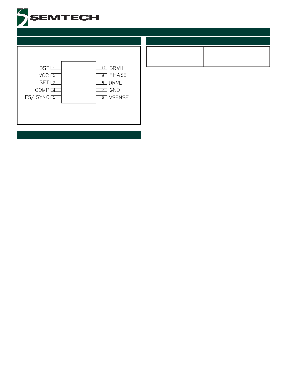
Ordering Information
Pin Descriptions
r
e
b
m
u
N
t
r
a
P
e
c
i
v
e
D
R
T
S
M
I
5
0
6
4
C
S
0
1
-
P
O
S
M
VCC: Positive supply rail for the IC. Bypass this pin to
GND with a 0.1 to 4.7µF low ESL/ESR ceramic capaci-
tor.
GND: All voltages are measured with respect to this pin.
All bypass and timing capacitors connected to GND should
have leads as short and direct as possible.
FS/SYNC: A capacitor from FS pin to GND sets the PWM
oscillator frequency. Use a high quality ceramic capacitor
with low ESL and ESR for best result. A minimum capaci-
tor value of 200pF ensures good accuracy and less sus-
ceptibility to circuit layout parasitics. When the FS is pulled
and held below 0.2V, its sleep mode operation is invoked.
The Sleepmode supply current is 10µA typical. The oscil-
lator and PWM are designed to provide practical opera-
tion up to 600kHz. In synchronous mode operation, a
low value resistor has to be connected between ground
and the timing capacitor. An external clock is then feed
into the resistor capacitor junction to override the inter-
nal clock.
VSENSE: This pin is the inverting input of the voltage
amplifier and serves as the output voltage feedback point
for the Buck converter. It senses the output voltage through
an external divider.
COMP: This is the output of the voltage amplifier. The
voltage at this output is inverted internally and connected
to the non-inverting input of the PWM comparator. A lead-
lag network around the voltage amplifier compensates for
the two pole LC filter characteristic inherent to voltage mode
control and is required in order to optimize the dynamic
performance of the voltage mode control loop.
ISET / PHASE: PHASE is connected to the junction be-
tween the two external power MOSFET transistors. The
voltage drop across the high side MOSFET during its con-
duction is compared with the voltage drop generated by
the internal 50µA current source and the external cur-
rent limit resistor connected between PHASE and Vin,
and forms the current limit comparator and logic sets
the PWM latch and terminates the output pulse. If the
converter output voltage drops below 68.75% of its nomi-
nal voltage, the controller stops switching and goes
through a soft start sequence. This prevents excess
power dissipation in the low side MOSFET during a short
circuit. The current limit threshold is set by the external
resistor between VCC and ISET.
BST: This pin connects the external charge pump, and
powers the high side MOSFET gate drive.
DRVH, DRVL: The output drivers are rated for 1A peak
currents. The PWM circuitry provides complementary drive
signals to the output stages. The cross conduction of
the external MOSFETs is prevented by monitoring the
voltage on the driver pins of the MOSFET pair in conjunc-
tion with a time delay optimized for FET turn-off charac-
teristics.
(10 Pin MSOP)
Note:
Only available in tape and reel packaging. A reel
contains 2500 devices.
Pin Configuration
Top View
5
2003 Semtech Corp.
www.semtech.com
SC4605
POWER MANAGEMENT
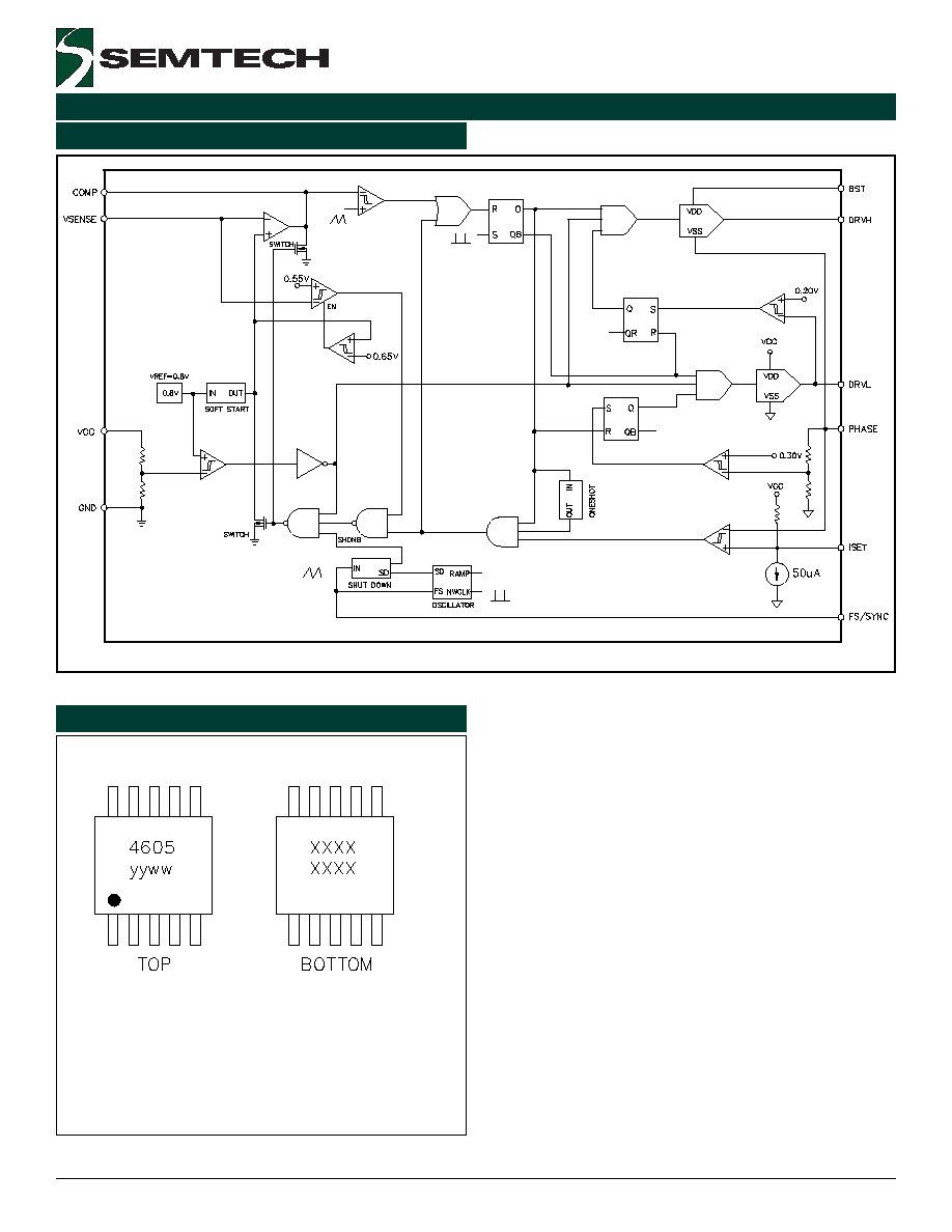
Block Diagram
Marking Information
yyww = Datecode (Example: 0012)
xxxx = Semtech Lot # (Example: E901
xxxx 01-1)