1
www.semtech.com
SC470
Synchronous Buck Controller for
Dynamic Load-Voltage Applications
POWER MANAGEMENT
September 27, 2005
Description
Features
Applications
The SC470 is a single output, constant on-time
synchronous-buck, pseudo-fixed frequency, PWM
controller intended for use in notebook computers and
other battery operated portable devices. Features
include high efficiency and fast dynamic response with
no minimum on-time. The excellent transient response
means that SC470 based solutions will require less
output capacitance than competing fixed frequency
converters.
The SC470 is specifically targeted for graphics processor
power supplies that require dynamic voltage transition,
with a tight 0.85% DC accuracy and a 20% OVP threshold.
The frequency is constant until a step-in load or line
voltage occurs, at which time the pulse density and
frequency will increase or decrease to counter the change
in output or input voltage. After the transient event, the
controller frequency will return to steady state operation.
At light loads, Power-Save Mode enables the SC470 to
skip PWM pulses for better efficiency.
The output voltage can be adjusted from 0.5V to VCCA.
The integrated gate drivers feature adaptive shoot-
through protection and soft switching. Additional features
include cycle-by-cycle current limit, digital soft-start, over-
voltage and under-voltage protection, and a PGD output.
Graphics Cards
Embedded Graphics Processors
High Performance Processors
Constant on-time for fast dynamic response
Programmable VOUT range = 0.5 ≠ VCCA
VBAT range = 1.8V ≠ 25V
DC current sense using low-side RDS(ON) sensing
or RSENSE in source of low-side MOSFET for
greater accuracy
Resistor programmable on-time
Cycle-by-cycle current limit
Digital soft-start
Combined EN and PSAVE functions
Over-voltage/under-voltage fault protection
and PGD output
20% OVP threshold for simpler dynamic voltage
transition circuitry
5µA typical shutdown current
Low quiescent power dissipation
14 lead TSSOP and 16 pin MLPQ (4mm x 4mm)
packages
Industrial temperature range
0.85% DC accuracy
Integrated gate drivers with soft-switching
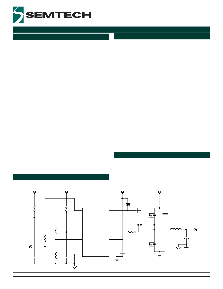
Typical Application Circuit
5VSUS
5VSUS
VBAT
R2
R1
RTON
PGOOD
R3
C4
1uF
VOUT
R4
L1
R2
C2
10uF
U1
SC470
EN/PSV
TON
VOUT
VCCA
FB
PGD
VSSA
PGND
DL
VDDP
ILIM
LX
DH
BST
C6
1uF
VOUT
D1
R1
10R
VBAT
+
C3
Q2
C1
0.1uF
Q1
C5
1nF
2
2005 Semtech Corp.
www.semtech.com
SC470
POWER MANAGEMENT
Absolute Maximum Ratings
(1)
Electrical Characteristics
Test Conditions: V
BAT
= 15V, EN/PSV = 5V, VCCA = VDDP = 5.0V, V
OUT
= 1.25V, R
TON
= 1M
, 0.1% Resistor Dividers.
r
e
t
e
m
a
r
a
P
s
n
o
i
t
i
d
n
o
C
C
∞
5
2
C
∞
5
2
1
o
t
C
∞
0
4
-
s
t
i
n
U
n
i
M
p
y
T
x
a
M
n
i
M
x
a
M
s
e
il
p
p
u
S
t
u
p
n
I
e
g
a
tl
o
V
t
u
p
n
I
A
C
C
V
0
.
5
5
.
4
5
.
5
V
e
g
a
tl
o
V
t
u
p
n
I
P
D
D
V
0
.
5
5
.
4
5
.
5
V
e
g
a
tl
o
V
t
u
p
n
I
N
I
V
s
n
0
0
8
>
e
m
it
ff
O
,
V
5
2
-
V
8
.
1
=
N
I
V
8
.
1
5
2
V
t
n
e
r
r
u
C
g
n
it
a
r
e
p
O
P
D
D
V
I
,t
n
i
o
p
n
o
it
a
l
u
g
e
r
>
B
F
D
A
O
L
A
0
=
0
7
0
5
1
A
µ
t
n
e
r
r
u
C
g
n
it
a
r
e
p
O
A
C
C
V
I
,t
n
i
o
p
n
o
it
a
l
u
g
e
r
>
B
F
D
A
O
L
A
0
=
0
0
7
0
0
1
1
A
µ
t
n
e
r
r
u
C
g
n
it
a
r
e
p
O
N
O
T
R
N
O
T
M
1
=
5
1
A
µ
t
n
e
r
r
u
C
n
w
o
d
t
u
h
S
V
0
=
V
S
P
/
N
E
5
-
0
1
-
A
µ
A
C
C
V
5
0
1
A
µ
N
I
V
+
P
D
D
V
0
1
A
µ
n
o
i
t
a
n
i
b
m
o
C
n
i
P
l
o
b
m
y
S
m
u
m
i
x
a
M
s
t
i
n
U
A
S
S
V
o
t
N
O
T
0
.
5
2
+
o
t
3
.
0
-
V
D
N
G
P
o
t
T
S
B
,
H
D
0
.
0
3
+
o
t
3
.
0
-
V
D
N
G
P
o
t
X
L
0
.
5
2
+
o
t
0
.
2
-
V
A
S
S
V
o
t
D
N
G
P
3
.
0
+
o
t
3
.
0
-
V
X
L
o
t
T
S
B
0
.
6
+
o
t
3
.
0
-
V
D
N
G
P
o
t
P
D
D
V
,
M
I
L
I
,
L
D
0
.
6
+
o
t
3
.
0
-
V
,
V
S
P
/
N
E
A
S
S
V
o
t
T
U
O
V
,
A
C
C
V
,
D
G
P
,
B
F
0
.
6
+
o
t
3
.
0
-
V
T
U
O
V
,
D
G
P
,
B
F
,
V
S
P
/
N
E
o
t
A
C
C
V
0
.
6
+
o
t
3
.
0
-
V
T
R
T
S
T
I
-
t
n
e
i
b
m
A
o
t
n
o
it
c
n
u
J
,
e
c
n
a
t
s
i
s
e
R
l
a
m
r
e
h
T
)
2
(
A
J
0
0
1
W
/
C
∞
T
R
T
L
M
I
-
t
n
e
i
b
m
A
o
t
n
o
it
c
n
u
J
,
e
c
n
a
t
s
i
s
e
R
l
a
m
r
e
h
T
)
2
(
A
J
1
3
W
/
C
∞
e
g
n
a
R
e
r
u
t
a
r
e
p
m
e
T
n
o
it
c
n
u
J
g
n
it
a
r
e
p
O
T
J
5
2
1
+
o
t
0
4
-
C
∞
e
g
n
a
R
e
r
u
t
a
r
e
p
m
e
T
e
g
a
r
o
t
S
T
G
T
S
0
5
1
+
o
t
5
6
-
C
∞
T
R
T
S
T
I
.
o
N
t
r
a
P
-
s
0
1
)
g
n
ir
e
d
l
o
S
(
e
r
u
t
a
r
e
p
m
e
T
d
a
e
L
T
D
A
E
L
0
0
3
C
∞
T
R
T
L
M
I
.
o
N
t
r
a
P
-
s
0
3
o
t
s
0
1
)
g
n
ir
e
d
l
o
S
(
w
o
lf
e
R
R
I
T
D
A
E
L
0
6
2
C
∞
Exceeding the specifications below may result in permanent damage to the device or device malfunction. Operation outside of the parameters
specified in the Electrical Characteristics section is not implied. Exposure to Absolute Maximum rated conditions for extended periods of time may
affect device reliability.
Notes:
1) This device is ESD sensitive. Use of standard ESD handling precautions is required.
2) Calculated from package in still air, mounted to 3" to 4.5", 4 layer FR4 PCB with thermal vias under the exposed pad per JESD51 standards.

3
2005 Semtech Corp.
www.semtech.com
SC470
POWER MANAGEMENT
Electrical Characteristics (Cont.)
r
e
t
e
m
a
r
a
P
s
n
o
i
t
i
d
n
o
C
5
2 ∞C
0
4
- ∞
5
2
1
o
t
C
∞C
s
t
i
n
U
n
i
M
p
y
T
x
a
M
n
i
M
x
a
M
r
e
ll
o
r
t
n
o
C
d
l
o
h
s
e
r
h
T
r
o
t
a
r
a
p
m
o
C
r
o
r
r
E
d
l
o
h
s
e
r
h
T
n
o
-
n
r
u
T
K
B
F
(
)
2
(
,
V
5
.
5
o
t
V
5
.
4
=
A
C
C
V
C
∞
0
T
A
C
∞
5
8
0
0
5
.
0
%
5
8
.
0
-
%
5
8
.
0
+
V
,
V
5
.
5
o
t
V
5
.
4
=
A
C
C
V
C
∞
0
4
-
T
A
C
∞
5
8
%
1
-
%
1
+
e
g
n
a
R
e
g
a
tl
o
V
t
u
p
t
u
O
e
d
o
M
t
s
u
j
d
A
5
.
0
A
C
C
V
V
V
,
e
m
i
T
-
n
O
T
A
B
V
5
.
2
=
R
N
O
T
M
1
=
1
6
7
1
7
9
4
1
5
2
0
2
s
n
R
N
O
T
k
0
0
5
=
6
3
9
6
9
7
6
7
0
1
s
n
e
m
i
T
ff
O
m
u
m
i
n
i
M
0
0
4
0
0
5
s
n
e
c
n
a
t
s
i
s
e
R
t
u
p
n
I
T
U
O
V
0
0
5
k
t
n
e
r
r
u
C
s
a
i
B
t
u
p
n
I
B
F
0
.
1
-
0
.
1
+
A
µ
g
n
i
s
n
e
S
t
n
e
r
r
u
C
-
r
e
v
O
t
n
e
r
r
u
C
k
n
i
S
M
I
L
I
h
g
i
H
L
D
0
1
0
.
9
0
.
1
1
A
µ
t
e
s
ff
O
r
o
t
a
r
a
p
m
o
C
t
n
e
r
r
u
C
M
I
L
I
-
D
N
G
P
0
1
-
0
1
V
m
E
V
A
S
P
d
l
o
h
s
e
r
h
T
g
n
i
s
s
o
r
C
-
o
r
e
Z
V
5
=
V
S
P
/
N
E
,
X
L
-
D
N
G
P
5
V
m
n
o
i
t
c
e
t
o
r
P
t
l
u
a
F
)
e
v
it
i
s
o
P
(
ti
m
i
L
t
n
e
r
r
u
C
)
3
(
R
,
X
L
-
D
N
G
P
M
I
L
I
k
5
=
0
5
5
3
5
6
V
m
R
,
X
L
-
D
N
G
P
M
I
L
I
k
0
1
=
0
0
1
0
8
0
2
1
V
m
R
,
X
L
-
D
N
G
P
M
I
L
I
k
0
2
=
0
0
2
0
7
1
0
3
2
V
m
)
e
v
it
a
g
e
N
(
ti
m
i
L
t
n
e
r
r
u
C
X
L
-
D
N
G
P
5
2
1
-
0
6
1
-
0
9
-
V
m
tl
u
a
F
e
g
a
tl
o
V
-
r
e
d
n
U
t
u
p
t
u
O
l
a
n
r
e
t
n
i
o
t
t
c
e
p
s
e
r
h
ti
W
.
e
c
n
e
r
e
f
e
r
0
3
-
0
4
-
5
2
-
%
tl
u
a
F
e
g
a
tl
o
V
-
r
e
v
O
t
u
p
t
u
O
l
a
n
r
e
t
n
i
o
t
t
c
e
p
s
e
r
h
ti
W
.
e
c
n
e
r
e
f
e
r
0
2
+
6
1
+
4
2
+
%
y
a
l
e
D
tl
u
a
F
e
g
a
tl
o
V
-
r
e
v
O
h
t
V
V
O
e
v
o
b
a
d
e
c
r
o
f
B
F
0
.
5
s
µ
e
g
a
tl
o
V
t
u
p
t
u
O
w
o
L
D
G
P
A
m
1
k
n
i
S
4
.
0
V
t
n
e
r
r
u
C
e
g
a
k
a
e
L
D
G
P
V
5
=
D
G
P
,
n
o
it
a
l
u
g
e
r
n
i
B
F
1
A
µ
d
l
o
h
s
e
r
h
T
V
U
D
G
P
l
a
n
r
e
t
n
i
o
t
t
c
e
p
s
e
r
h
ti
W
.
e
c
n
e
r
e
f
e
r
0
1
-
2
1
-
8
-
%

4
2005 Semtech Corp.
www.semtech.com
SC470
POWER MANAGEMENT
Notes:
(1) Calculated from package in still air, mounted to 3" x 4.5", 4 layer FR4 PCB with thermal vias under the exposed pad per JESD51 standards.
(2) When the inductor is in continuous and discontinuous conduction mode, the output voltage will have a DC regulation level higher than the
error-comparator threshold by 50% of the ripple voltage. This voltage will vary slightly with load and VBAT.
(3) Using a current sense resistor, this measurement relates to PGND minus the voltage of the source on the low-side MOSFET. These values
guaranteed by the ILIM Source Current and Current Comparator Offset tests.
(4) clks = switching cycles.
Electrical Characteristics (Cont.)
r
e
t
e
m
a
r
a
P
s
n
o
i
t
i
d
n
o
C
C
∞
5
2
C
∞
5
2
1
o
t
C
∞
0
4
-
s
t
i
n
U
n
i
M
p
y
T
x
a
M
n
i
M
x
a
M
)
.
t
n
o
C
(
n
o
i
t
c
e
t
o
r
P
t
l
u
a
F
y
a
l
e
D
tl
u
a
F
D
G
P
.
w
o
d
n
i
w
D
G
P
e
d
i
s
t
u
o
d
e
c
r
o
f
B
F
0
.
5
s
µ
e
g
a
tl
o
v
r
e
d
n
U
A
C
C
V
d
l
o
h
s
e
r
h
T
)
s
i
s
e
r
e
t
s
y
H
V
m
0
0
1
(
g
n
il
l
a
F
0
.
4
7
.
3
3
.
4
V
t
u
o
k
c
o
L
e
r
u
t
a
r
e
p
m
e
T
r
e
v
O
0
1
O
s
i
s
e
r
e
t
s
y
H
C
5
6
1
C
s
t
u
p
t
u
O
/
s
t
u
p
n
I
e
g
a
tl
o
V
w
o
L
t
u
p
n
I
c
i
g
o
L
w
o
l
V
S
P
/
N
E
2
.
1
V
e
g
a
tl
o
V
h
g
i
H
t
u
p
n
I
c
i
g
o
L
w
o
l
V
S
P
,
h
g
i
H
N
E
)
g
n
it
a
o
l
F
n
i
P
(
0
.
2
V
e
g
a
tl
o
V
h
g
i
H
t
u
p
n
I
c
i
g
o
L
h
g
i
h
V
S
P
/
N
E
1
.
3
V
t
u
p
n
I
e
v
a
S
r
e
w
o
P
/
e
l
b
a
n
E
e
c
n
a
t
s
i
s
e
R
A
C
C
V
o
t
p
u
ll
u
P
R
5
.
1
M
A
S
S
V
o
t
n
w
o
d
ll
u
P
R
1
M
t
r
a
t
S
t
f
o
S
e
m
i
T
p
m
a
R
t
r
a
t
S
-
tf
o
S
h
g
i
h
D
G
P
o
t
h
g
i
h
V
S
P
/
N
E
0
4
4
s
k
l
c
)
4
(
e
m
i
T
k
n
a
l
B
e
g
a
tl
o
V
-
r
e
d
n
U
h
g
i
h
V
U
o
t
h
g
i
h
V
S
P
/
N
E
0
4
4
s
k
l
c
)
4
(
s
r
e
v
i
r
D
e
t
a
G
e
m
i
T
d
a
e
D
g
n
i
s
ir
L
D
r
o
H
D
0
3
s
n
e
c
n
a
t
s
i
s
e
R
n
w
o
D
-l
l
u
P
L
D
w
o
l
L
D
8
.
0
6
.
1
t
n
e
r
r
u
C
k
n
i
S
L
D
V
5
.
2
=
L
D
1
.
3
A
e
c
n
a
t
s
i
s
e
R
p
U
-l
l
u
P
L
D
h
g
i
h
L
D
2
4
t
n
e
r
r
u
C
e
c
r
u
o
S
L
D
V
5
.
2
=
L
D
3
.
1
A
e
c
n
a
t
s
i
s
e
R
n
w
o
D
-l
l
u
P
H
D
V
5
=
X
L
-
T
S
B
,
w
o
l
H
D
2
4
e
c
n
a
t
s
i
s
e
R
p
U
-l
l
u
P
H
D
V
5
=
X
L
-
T
S
B
,
h
g
i
h
H
D
2
4
t
n
e
r
r
u
C
e
c
r
u
o
S
/
k
n
i
S
H
D
V
5
.
2
=
H
D
3
.
1
A
5
2005 Semtech Corp.
www.semtech.com
SC470
POWER MANAGEMENT
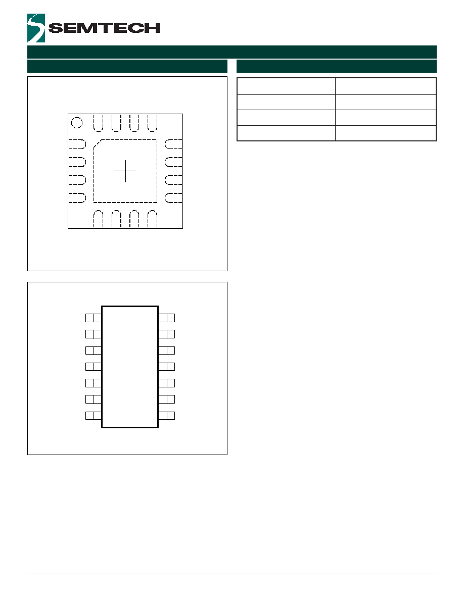
Pin Configuration
Ordering Information
TOP VIEW
1
2
3
4
12
11
10
9
16
15
14
13
5
6
7
8
MLPQ16: 4X4 BODY
T
TO
N
EN/
P
S
V
NC
BS
T
DH
LX
ILIM
VDDP
VOUT
VCCA
FB
PGD
NC
V
SSA
PG
N
D
DL
E
C
I
V
E
D
)
1
(
E
G
A
K
C
A
P
T
R
T
L
M
I
0
7
4
C
S
)
3
(
)
2
(
6
1
-
Q
P
L
M
T
R
T
S
T
I
0
7
4
C
S
)
3
(
)
2
(
4
1
-
P
O
S
S
T
B
V
E
0
7
4
C
S
)
4
(
d
r
a
o
B
n
o
it
a
u
l
a
v
E
Notes:
(1) Only available in tape and reel packaging. A reel contains
2500 devices.
(2) This product is fully WEEE and RoHS compliant.
(3) Lead-free product. This product is J-STD-020B compliant and
all homogeneous subcomponents are RoHS compliant.
(4) Part-specific evaluation boards - consult factory for availability.
1
2
3
4
5
6
7
BST
EN/PSV
TOP VIEW
(14 Pin TSSOP)
13
12
14
11
10
DH
TON
LX
VOUT
ILIM
VCCA
VDDP
FB
DL
PGD
PGND
VSSA
9
8

6
2005 Semtech Corp.
www.semtech.com
SC470
POWER MANAGEMENT
e
m
a
N
n
i
P
#
6
1
-
Q
P
L
M
#
4
1
-
P
O
S
S
T
n
o
i
t
c
n
u
F
n
i
P
T
U
O
V
1
3
.
d
a
o
l
e
h
t
t
a
T
U
O
V
o
t
t
c
e
n
n
o
C
.t
u
p
n
i
e
s
n
e
s
e
g
a
tl
o
v
t
u
p
t
u
O
A
C
C
V
2
4
r
e
tl
if
C
R
F
µ
1
/
m
h
O
0
1
a
e
s
U
.
y
l
p
p
u
s
g
o
l
a
n
a
e
h
t
r
o
f
t
u
p
n
i
e
g
a
tl
o
v
y
l
p
p
u
S
.
A
S
S
V
o
t
S
U
S
V
5
m
o
r
f
B
F
3
5
t
e
s
o
t
A
S
S
V
o
t
T
U
O
V
m
o
r
f
r
e
d
i
v
i
d
r
o
t
s
i
s
e
r
a
o
t
t
c
e
n
n
o
C
.t
u
p
n
i
k
c
a
b
d
e
e
F
.
A
C
C
V
d
n
a
V
5
.
0
n
e
e
w
t
e
b
e
g
a
tl
o
v
t
u
p
t
u
o
e
h
t
D
G
P
4
6
e
l
c
y
c
k
c
o
l
c
d
e
x
if
a
r
e
tf
a
h
g
i
h
s
e
o
G
.t
u
p
t
u
o
S
O
M
N
n
i
a
r
d
n
e
p
o
d
o
o
G
r
e
w
o
P
.
p
u
-
r
e
w
o
p
g
n
i
w
o
ll
o
f
)
s
e
l
c
y
c
0
4
4
(
y
a
l
e
d
C
N
5
-
.t
c
e
n
n
o
C
o
N
A
S
S
V
6
7
t
u
p
t
u
o
e
h
t
f
o
m
o
tt
o
b
e
h
t
o
t
t
c
e
n
n
o
C
.
y
r
ti
u
c
r
i
c
g
o
l
a
n
a
r
o
f
e
c
n
e
r
e
f
e
r
d
n
u
o
r
G
.r
o
ti
c
a
p
a
c
D
N
G
P
7
8
.
d
n
u
o
r
g
r
e
w
o
P
L
D
8
9
.
h
c
ti
w
s
T
E
F
S
O
M
e
d
i
s
w
o
l
e
h
t
r
o
f
t
u
p
t
u
o
e
v
ir
d
e
t
a
G
P
D
D
V
9
0
1
F
µ
1
a
h
ti
w
n
i
p
s
i
h
t
e
l
p
u
o
c
e
D
.
s
r
e
v
ir
d
e
t
a
g
e
h
t
r
o
f
t
u
p
n
i
e
g
a
tl
o
v
y
l
p
p
u
s
V
5
+
.
D
N
G
P
o
t
r
o
ti
c
a
p
a
c
c
i
m
a
r
e
c
M
I
L
I
0
1
1
1
)
n
o
(
S
D
R
r
o
f
T
E
F
S
O
M
e
d
i
s
-
w
o
l
f
o
n
i
a
r
d
o
t
t
c
e
n
n
o
C
.t
u
p
n
i
ti
m
il
t
n
e
r
r
u
C
g
n
i
s
n
e
s
d
l
o
h
s
e
r
h
t
a
h
g
u
o
r
h
t
g
n
i
s
n
e
s
r
o
f
r
o
t
s
i
s
e
r
e
c
r
u
o
s
e
h
t
r
o
,
g
n
i
s
n
e
s
.r
o
t
s
i
s
e
r
X
L
1
1
2
1
)
r
o
t
c
u
d
n
i
t
u
p
t
u
o
e
h
t
d
n
a
s
T
E
F
S
O
M
m
o
tt
o
b
d
n
a
p
o
t
f
o
n
o
it
c
n
u
j(
e
d
o
n
e
s
a
h
P
.
n
o
it
c
e
n
n
o
c
H
D
2
1
3
1
.
h
c
ti
w
s
T
E
F
S
O
M
e
d
i
s
h
g
i
h
e
h
t
r
o
f
t
u
p
t
u
o
e
v
ir
d
e
t
a
G
T
S
B
3
1
4
1
.
e
v
ir
d
e
t
a
g
e
d
i
s
h
g
i
h
e
h
t
r
o
f
n
o
it
c
e
n
n
o
c
r
o
ti
c
a
p
a
c
t
s
o
o
B
C
N
4
1
-
.t
c
e
n
n
o
C
o
N
V
S
P
/
N
E
5
1
1
p
u
-l
l
u
P
.
C
I
e
h
t
n
w
o
d
t
u
h
s
o
t
A
S
S
V
o
t
n
w
o
d
ll
u
P
.
t
u
p
n
i
e
v
a
S
r
e
w
o
P
/
e
l
b
a
n
E
d
n
a
C
I
e
h
t
e
l
b
a
n
e
o
t
t
a
o
l
F
.
e
d
o
m
E
V
A
S
P
e
t
a
v
it
c
a
d
n
a
C
I
e
h
t
e
l
b
a
n
e
o
t
A
S
S
V
o
t
s
s
a
p
y
b
,
d
e
t
a
o
lf
fI
.
)
M
C
C
(
e
d
o
m
n
o
it
c
u
d
n
o
c
s
u
o
n
it
n
o
c
e
t
a
v
it
c
a
.r
o
ti
c
a
p
a
c
c
i
m
a
r
e
c
F
n
0
1
a
h
ti
w
N
O
T
6
1
2
o
t
d
n
a
,
N
O
T
R
,r
o
t
s
i
s
e
r
p
u
ll
u
p
a
h
g
u
o
r
h
t
T
A
B
V
e
s
n
e
s
o
t
d
e
s
u
s
i
n
i
p
s
i
h
T
r
o
ti
c
a
p
a
c
c
i
m
a
r
e
c
F
n
1
a
h
ti
w
n
i
p
s
i
h
t
s
s
a
p
y
B
.
e
m
it
-
n
o
T
E
F
S
O
M
p
o
t
e
h
t
t
e
s
.
A
S
S
V
o
t
L
A
M
R
E
H
T
D
A
P
T
-
e
l
p
it
l
u
m
g
n
i
s
u
e
n
a
l
p
d
n
u
o
r
g
o
t
t
c
e
n
n
o
C
.
s
e
s
o
p
r
u
p
g
n
i
k
n
i
s
t
a
e
h
r
o
f
d
a
P
.
y
ll
a
n
r
e
t
n
i
d
e
t
c
e
n
n
o
c
t
o
N
.
s
a
i
v
Pin Descriptions
7
2005 Semtech Corp.
www.semtech.com
SC470
POWER MANAGEMENT
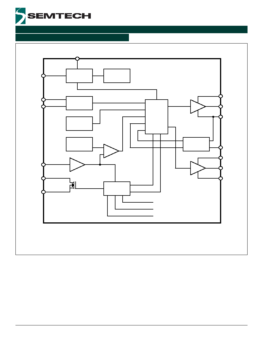
Block Diagram
+
-
REF + 20%
VSSA
X3
OV
DL
PGD
DH
CONTROL
ZERO I
UV
TOFF
VDDP
POR / SS
BST
VOUT
HI
EN/SPV
LX
ILIM
VCCA
MONITOR
1.5V REF
REF - 30%
FAULT
ON
FB
LOGIC
OT
TON
ISENSE
PWM
TON
OFF
PGND
REF - 10%
LO
OC
Figure 1: SC470 Block Diagram

8
2005 Semtech Corp.
www.semtech.com
SC470
POWER MANAGEMENT
+5V Bias Supplies
The SC470 requires an external +5V bias supply in
addition to the battery. If stand-alone capability is
required, the +5V supply can be generated with an
external linear regulator such as the Semtech LP2951.
For optimal operation, the controller has its own ground
reference, VSSA, which should be tied by a single trace
to PGND at the negative terminal of the output
capacitor (see Layout Guidelines). All external compo-
nents referenced to VSSA in the Typical Applications Cir-
cuit on Page 1 should be connected to VSSA. The supply
decoupling capacitor should be tied directly between the
VCCA and VSSA pins. A 10
resistor should be used to
decouple VCCA from the main VDDP supply. PGND can
then be a separate plane which is not used for routing
traces. All PGND connections are connected directly to
the ground plane with special attention given to avoiding
indirect connections which may create ground loops. As
mentioned above, VSSA must be connected to the PGND
plane at the negative terminal of the output capacitor
only. The VDDP input provides power to the upper and
lower gate drivers. A decoupling capacitor is required.
No series resistor between VDDP and 5V is required. See
Layout Guidelines for more details.
Pseudo-Fixed Frequency Constant On-Time PWM
Controller
The PWM control architecture consists of a constant on-
time, pseudo-fixed frequency PWM controller (see Figure
1, Block Diagram, page 7). The output ripple voltage
developed across the output filter capacitor's ESR
provides the PWM ramp signal eliminating the need for a
current sense resistor. The high-side switch on-time is
determined by a one-shot whose period is directly
proportional to output voltage and inversely proportional
to input voltage. A second one-shot sets the minimum
off-time which is typically 400ns.
On-Time One-Shot (t
ON
)
The on-time one-shot comparator has two inputs. One
input looks at the output voltage, while the other input
samples the input voltage and converts it to a current.
This input voltage-proportional current is used to charge
an internal on-time capacitor. The on-time is the time
required for the voltage on this capacitor to charge from
zero volts to VOUT, thereby making the on-time of the
high-side switch directly proportional to output voltage
and inversely proportional to input voltage. This
implementation results in a nearly constant switching
frequency without the need for a clock generator.
For VOUT < 3.3V:
ns
50
V
V
)
10
x
37
R
(
10
x
3
.
3
t
BAT
OUT
3
TON
12
ON
+
∑
+
∑
=
-
For 3.3V
VOUT
5V:
ns
50
V
V
)
10
x
37
R
(
10
x
3
.
3
85
.
0
t
BAT
OUT
3
TON
12
ON
+
∑
+
∑
∑
=
-
R
TON
is a resistor connected from the input supply (VBAT)
to the TON
pin. Due to the high impedance of this
resistor, the TON pin should always be bypassed to VSSA
using a 1nF ceramic capacitor.
Enable & Psave
The EN/PSV pin enables the supply. When EN/PSV is
tied to VCCA the controller is enabled and power save
will also be enabled. When the EN/PSV pin is tri-stated,
an internal pull-up will activate the controller and power
save will be disabled. If PSAVE is enabled, the SC470
PSAVE comparator will look for the inductor current to
cross zero on eight consecutive switching cycles by
comparing the phase node (LX) to PGND. Once observed,
the controller will enter power save and turn off the low
side MOSFET when the current crosses zero. To improve
light-load efficiency and add hysteresis, the on-time is
increased by 50% in power save. The efficiency
improvement at light-loads more than offsets the
disadvantage of slightly higher output ripple. If the
inductor current does not cross zero on any switching
cycle, the controller will immediately exit power save.
Since the controller counts zero crossings, the converter
can sink current as long as the current does not cross
zero on eight consecutive cycles. This allows the output
voltage to recover quickly in response to negative load
steps even when PSAVE is enabled.
Application Information
9
2005 Semtech Corp.
www.semtech.com
SC470
POWER MANAGEMENT
Application Information (Cont.)
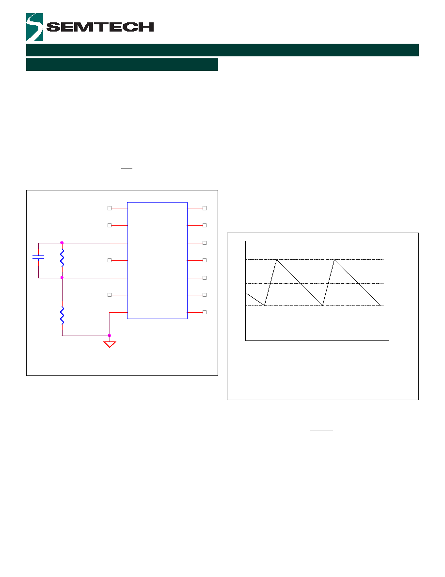
Output Voltage Selection
The output voltage is set by the feedback resistors R3 &
R7 of Figure 2 below. The internal reference is 1.5V, so
the voltage at the feedback pin is multiplied by three to
match the 1.5V reference. Therefore, the
output can be set to a minimum of 0.5V. The equation
for setting the output voltage is:
Figure 2: Setting The Output Voltage
Current Limit Circuit
Current limiting of the SC470 can be accomplished in
two ways. The on-state resistance of the low-side MOSFET
can be used as the current sensing element or sense
resistors in series with the low-side source can be used
if greater accuracy is desired. R
DS(ON)
sensing is more
efficient and less expensive. In both cases, the R
ILIM
resistor between the ILIM pin and LX pin set the over
current threshold. This resistor R
ILIM
is connected to a
10
µ
A current source within the SC470 which is turned
on when the low side MOSFET turns on. When the
voltage drop across the sense resistor or low side
MOSFET equals the voltage across the RILIM resistor,
positive current limit will activate. The high-side MOSFET
will not be turned on until the voltage drop across the
sense element (resistor or MOSFET) falls below the
voltage across the R
ILIM
resistor. In an extreme over-
current situation, the top MOSFET will never turn back
on and eventually the part will latch off due to output
undervoltage (see Output Under-voltage Protection).
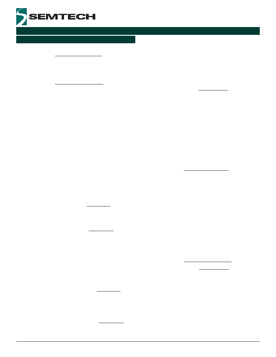
The current sensing circuit actually regulates the
inductor valley current (see Figure 3). This means that if
the current limit is set to 10A, the peak current through
the inductor would be 10A plus the peak ripple current,
and the average current through the inductor would be
10A plus 1/2 the peak-to-peak ripple current. The
equations for setting the valley current and calculating
the average current through the inductor are shown
below:
I
LIMIT
I
LOAD
I
PEAK
I
N
DU
CT
O
R
CUR
R
E
N
T
TIME
Valley Current-Limit Threshold Point
Figure 3: Valley Current Limiting
The equation for the current limit threshold is as follows:
A
R
R
10e
I
SENSE
ILIM
6
-
LIMIT
∑
=
Where (referring to Figure 8 on Page 17) R
ILIM
is R4 and
R
SENSE
is the R
DS(ON)
of Q2.
For resistor sensing, a sense resistor is placed between
the source of Q2 and PGND. The current through the
source sense resistor develops a voltage that opposes
the voltage developed across R
ILIM
. When the voltage
developed across the R
SENSE
resistor reaches the voltage
R3
20k0
R7
20k0
EN/PSV
TON
VOUT
VCCA
FB
PGD
VSSA
PGND
DL
VDDP
ILIM
LX
DH
BST
U1
SC470
VOUT
0402
0402
C5
56p
0402
5
.
0
7
R
3
R
1
V
OUT
∑
+
=

10
2005 Semtech Corp.
www.semtech.com
SC470
POWER MANAGEMENT
drop across R
ILIM
, a positive over-current exists and the
high side MOSFET will not be allowed to turn on. When
using an external sense resistor R
SENSE
is the resistance
of the sense resistor.
The current limit circuitry also protects against negative
over-current (i.e., when the current is flowing from the
load to PGND through the inductor and bottom MOSFET).
In this case, when the bottom MOSFET is turned on, the
phase node, LX, will be higher than PGND initially. The
SC470 monitors the voltage at LX, and if it is greater
than a set threshold voltage of 140mV (nom.) the
bottom MOSFET is turned off. The device then waits for
approximately 2.5µs and then DL goes high for 300ns
(typ.) once more to sense the current. This repeats until
either the over-current condition goes away or the part
latches off due to output over-voltage (see Output
Over-voltage Protection).
Power Good Output
The power good output is an open-drain output and
requires a pull-up resistor. When the output voltage is
20% above or 10% below its set voltage, PGD gets pulled
low. It is held low until the output voltage returns to within
+
20%/-10% of the output set voltage. PGD is also held
low during start-up and will not be allowed to transition
high until soft-start is over (440 switching cycles) and
the output reaches 90% of its set voltage. There is a 5µs
delay built into the PGD circuitry to prevent false
transitions.
Output Over-Voltage Protection
When the output exceeds 20% of the its set voltage the
low-side MOSFET is latched on. It stays latched on and
the controller is latched off until reset. There is a 5µs
delay built into the OV protection circuit to
prevent false transitions.
Output Under-Voltage Protection
When the output is 30% below its set voltage the output
is latched in a tri-stated condition. It stays latched and
the controller is latched off until reset. There is a 5µs
delay built into the UV protection circuit to
prevent false transitions. Note: to reset from any fault,
VCCA or EN/PSV must be toggled.
Application Information (Cont.)
POR, UVLO and Softstart
An internal power-on reset (POR) occurs when VCCA ex-
ceeds 3V, resetting the fault latch and soft-start counter,
and preparing the PWM for switching. VCCA
under-volt-
age lockout (UVLO) circuitry inhibits switching and forces
the DL gate driver high until VCCA rises above 4.2V. At
this time the circuit will come out of UVLO and begin
switching, and with the soft-start circuit enabled, will pro-
gressively limit the output current (by limiting the current
out of the ILIM pin) over a predetermined time period of
440 switching cycles.
The ramp occurs in four steps:
1) 110 cycles at 25% ILIM with double minimum off-time
(for purposes of the on-time one-shot there is an internal
positive offset of 120mV to VOUT during this period to
aid in start-up).
2) 110 cycles at 50% ILIM with normal minimum off-time.
3) 110 cycles at 75% ILIM with normal minimum off-time.
4) 110 cycles at 100% ILIM with normal minimum
off-time.
At this point the output under-voltage and power good
circuitry is enabled. There is 100mV of hysteresis built
into the UVLO circuit and when VCCA
falls to 4.1V (nom.)
the output drivers are shut down and tristated.
MOSFET Gate Drivers
The DH and DL drivers are optimized for driving
moderate-sized high-side, and larger low-side power
MOSFETs. An adaptive dead-time circuit monitors the DL
output and prevents the high-side MOSFET from turning
on until DL is fully off (below ~1V). Conversely, it
monitors the phase node, LX, to determine the state of
the high side MOSFET, and prevents the low-side MOSFET
from turning on until DH is fully off (LX below ~1V). Note:
Be sure there is low resistance and low inductance be-
tween the DH and DL outputs to the gate of each
MOSFET.
Dropout Performance
The output voltage adjust range for continuous-
conduction operation is limited by the fixed 550ns

11
2005 Semtech Corp.
www.semtech.com
SC470
POWER MANAGEMENT
(maximum) minimum off-time one-shot. For best dropout
performance, use the slowest on-time setting of 200kHz.
When working with low input voltages, the duty-factor
limit must be calculated using worst-case values for on
and off times. The IC duty-factor limitation is given by:
)
MAX
(
OFF
t
)
MIN
(
ON
t
)
MIN
(
ON
t
DUTY
+
=
Be sure to include inductor resistance and MOSFET on-
state voltage drops when performing worst-case dropout
duty-factor calculations.
470 System DC Accuracy
Two IC parameters affect system DC accuracy, the error
comparator threshold voltage variation and the switching
frequency variation with line and load. The error
comparator threshold does not drift significantly with
supply and temperature. Thus, the error comparator
contributes 0.85% or less to DC system inaccuracy.
Board components and layout also influence DC
accuracy. The use of 1% feedback resistors contribute
1%. If tighter DC accuracy is required use 0.1% feedback
resistors.
The on-pulse in the SC470 is calculated to give a pseudo-
fixed frequency. Nevertheless, some frequency variation
with line and load can be expected. This variation changes
the output ripple voltage. Because constant on-
regulators regulate to the valley of the output ripple, Ω
of the output ripple appears as a DC regulation error.
For example, if the feedback resistors are chosen to
divide down the output by a factor of five, the valley of
the output ripple will be VOUT. For example: if VOUT is
2.5V and the ripple is 50mV with VBAT = 6V, then the
measured DC output will be 2.525V. If the ripple increases
to 80mV with VBAT = 25V, then the measured DC output
will be 2.540V.
The output inductor value may change with current. This
will change the output ripple and thus the DC output
voltage. It will not change the frequency.
Switching frequency variation with load can be minimized
by choosing MOSFETs with lower R
DS(ON)
. High R
DS(ON)
MOSFETs will cause the switching frequency to increase
as the load current increases. This will reduce the ripple
and thus the DC output voltage.
Design Procedure
Prior to designing an output and making component
selections, it is necessary to determine the input voltage
range and the output voltage specifications. For purposes
of demonstrating the procedure the output for the
schematic in Figure 8 on Page 17 will be designed.
The maximum input voltage (V
BAT(MAX)
) is determined by
the highest AC adaptor voltage. The minimum input
voltage (V
BAT(MIN)
) is determined by the lowest battery
voltage after accounting for voltage drops due to
connectors, fuses and battery selector switches. For the
purposes of this design we will use a V
BAT
range of 8V to
20V.
Four parameters are needed for the output:
1) Nominal output voltage, V
OUT
(we will use 1.2V).
2) Static (or DC) tolerance, TOL
ST
(we will use +/-4%).
3) Transient tolerance, TOL
TR
and size of transient (we
will use +/-8% for purposes of this demonstration).
4) Maximum output current, I
OUT
(we will design for 6A).
Switching frequency determines the trade-off between
size and efficiency. Increased frequency increases the
switching losses in the MOSFETs, since losses are a
function of VIN
2
, knowing the maximum input voltage and
budget for MOSFET switches usually dictates where the
design ends up. A default R
tON
value of 1M
is suggested
as a starting point, but this is not set in stone. The first
thing to do is to calculate the on-time, t
ON
, at V
BAT(MIN)
and
V
BAT(MAX)
, since this depends only upon V
BAT
, V
OUT
and R
tON
.
For V
OUT
< 3.3V:
(
)
s
10
50
V
V
10
37
R
10
3
.
3
t
9
)
MIN
(
BAT
OUT
3
tON
12
)
MIN
(
VBAT
_
ON
-
-
∑
+
∑
∑
+
∑
∑
=
and,
(
)
s
10
50
V
V
10
37
R
10
3
.
3
t
9
)
MAX
(
BAT
OUT
3
tON
12
)
MAX
(
VBAT
_
ON
-
-
∑
+
∑
∑
+
∑
∑
=
From these values of t
ON
we can calculate the nominal
switching frequency as follows:
Application Information (Cont.)
12
2005 Semtech Corp.
www.semtech.com
SC470
POWER MANAGEMENT
Application Information (Cont.)
(
)
Hz
t
V
V
f
)
MIN
(
VBAT
_
ON
)
MIN
(
BAT
OUT
)
MIN
(
VBAT
_
SW
∑
=
and,
(
)
Hz
t
V
V
f
)
MAX
(
VBAT
_
ON
)
MAX
(
BAT
OUT
)
MAX
(
VBAT
_
SW
∑
=
t
ON
is generated by a one-shot comparator that samples
V
BAT
via R
tON
, converting this to a current. This current is
used to charge an internal 3.3pF capacitor to V
OUT
. The
equations on page 11 reflect this along with any internal
components or delays that influence t
ON
.
For our example we select R
tON
= 1M
:
t
ON_VBAT(MIN)
= 563ns and t
ON_VBAT(MAX)
= 255ns
f
SW_VBAT(MIN)
= 266kHz and f
SW_VBAT(MAX)
= 235kHz
Now that we know t
ON
we can calculate suitable values
for the inductor. To do this we select an acceptable
inductor ripple current. The calculations below assume
50% of I
OUT
which will give us a starting place.
(
)
(
)
H
I
5
.
0
t
V
V
L
OUT
)
MIN
(
VBAT
_
ON
OUT
)
MIN
(
BAT
)
MIN
(
VBAT
∑
∑
-
=
and,
(
)
(
)
H
I
5
.
0
t
V
V
L
OUT
)
MAX
(
VBAT
_
ON
OUT
)
MAX
(
BAT
)
MAX
(
VBAT
∑
∑
-
=
For our example:
L
VBAT(MIN)
= 1.3µH and L
VBAT(MAX)
= 1.6µH
We will select an inductor value of 2.2µH to reduce the
ripple current, which can be calculated as follows:
(
)
P
P
)
MIN
(
VBAT
_
ON
OUT
)
MIN
(
BAT
)
MIN
(
VBAT
_
RIPPLE
A
L
t
V
V
I
-
∑
-
=
and,
(
)
P
P
)
MAX
(
VBAT
_
ON
OUT
)
MAX
(
BAT
)
MAX
(
VBAT
_
RIPPLE
A
L
t
V
V
I
-
∑
-
=
For our example:
I
RIPPLE_VBAT(MIN)
= 1.74A
P-P
and I
RIPPLE_VBAT(MAX)
= 2.18A
P-P
From this we can calculate the minimum inductor
current rating for normal operation:
)
MIN
(
)
MAX
(
VBAT
_
RIPPLE
)
MAX
(
OUT
)
MIN
(
INDUCTOR
A
2
I
I
I
+
=
For our example:
I
INDUCTOR(MIN)
= 7.1A
(MIN)
Next we will calculate the maximum output capacitor
equivalent series resistance (ESR). This is determined by
calculating the remaining static and transient tolerance
allowances. Then the maximum ESR is the smaller of the
calculated static ESR (R
ESR_ST(MAX)
) and transient ESR
(R
ESR_TR(MAX)
):
(
)
Ohms
I
2
ERR
ERR
R
)
MAX
(
VBAT
_
RIPPLE
DC
ST
)
MAX
(
ST
_
ESR
∑
-
=
Where ERR
ST
is the static output tolerance and ERR
DC
is
the DC error. The DC error will be 0.85% plus the
tolerance of the feedback resistors, thus 1.85% total
for 1% feedback resistors.
For our example:
ERR
ST
= 48mV and ERR
DC
= 22mV, therefore,
R
ESR_ST(MAX)
= 24m
(
)
Ohms
2
I
I
ERR
ERR
R
)
MAX
(
VBAT
_
RIPPLE
OUT
DC
TR
)
MAX
(
TR
_
ESR
+
-
=
Where ERR
TR
is the transient output tolerance. Note that
this calculation assumes that the worst case load
transient is full load. For half of full load, divide the I
OUT
term by 2.
For our example:
ERR
TR
= 96mV and ERR
DC
= 22mV, therefore,

13
2005 Semtech Corp.
www.semtech.com
SC470
POWER MANAGEMENT
Application Information (Cont.)
R
ESR_TR(MAX)
= 10.4m
for a full 6A load transient
Wewill select a value of 12.5m
maximum for our
design, which would be achieved by using two 25m
output capacitors in parallel.
Note that for constant-on converters there is a mini-
mum ESR requirement for stability which can be
calculated as follows:
SW
OUT
)
MIN
(
ESR
f
C
2
3
R
∑
∑
∑
=
This criteria should be checked once the output
capacitance has been determined.
Now that we know the output ESR we can calculate
the output ripple voltage:
P
P
)
MAX
(
VBAT
_
RIPPLE
ESR
)
MAX
(
VBAT
_
RIPPLE
V
I
R
V
-
∑
=
and,
P
P
)
MIN
(
VBAT
_
RIPPLE
ESR
)
MIN
(
VBAT
_
RIPPLE
V
I
R
V
-
∑
=
For our example:
V
RIPPLE_VBAT(MAX)
= 27mV
P-P
and V
RIPPLE_VBAT(MIN)
= 22mV
P-P
Note that in order for the device to regulate in a
controlled manner, the ripple content at the feedback
pin, V
FB
, should be approximately 15mV
P-P
at minimum
V
BAT
, and worst-case no smaller than 10mV
P-P
. If
V
RIPPLE_VBAT(MIN)
is less than 15mV
P-P
the above component
values should be revisited in order to improve this. Quite
often a small capacitor, C
TOP
, is required in parallel with
the top feedback resistor, R
TOP
, in order to ensure that
V
FB
is large enough. C
TOP
should not be greater than
100pF. The value of C
TOP
can be calculated as follows,
where R
BOT
is the bottom feedback resistor. Firstly
calculating the value of Z
TOP
required:
(
)
Ohms
015
.
0
V
015
.
0
R
Z
)
MIN
(
VBAT
_
RIPPLE
BOT
TOP
-
∑
=
Secondly calculating the value of C
TOP
required to achieve
this:
For our example we will use R
TOP
= 20.0k
and
R
BOT
= 14.3k
, therefore:
Z
TOP
= 6.67k
and C
TOP
= 60pF
We will select a value of C
TOP
= 56pF. Calculating the
value of V
FB
based upon the selected C
TOP
:
P
P
TOP
)
MIN
(
VBAT
_
SW
TOp
BOT
BOT
)
MIN
(
VBAT
_
RIPPLE
)
MIN
(
VBAT
_
FB
V
C
f
2
R
1
1
R
R
V
V
-
∑
∑
∑
+
+
∑
=
For our example:
V
FB_VBAT(MIN)
= 14.8mV
P-P
- good
Next we need to calculate the minimum output
capacitance required to ensure that the output voltage
does not exceed the transient maximum limit, POSLIM
TR
,
starting from the actual static maximum, V
OUT_ST_POS
, when
a load release occurs:
V
ERR
V
V
DC
OUT
POS
_
ST
_
OUT
+
=
For our example:
V
OUT_ST_POS
= 1.222V
V
TOL
V
POSLIM
TR
OUT
TR
∑
=
Where TOL
TR
is the transient tolerance. For our
example:
POSLIM
TR
= 1.296V
The minimum output capacitance is calculated as
follows:
(
)
F
V
POSLIM
2
I
I
L
C
2
POS
_
ST
_
OUT
2
TR
2
)
MAX
(
VBAT
_
RIPPLE
OUT
)
MIN
(
OUT
-
+
∑
=
F
f
2
R
1
Z
1
C
)
MIN
(
VBAT
_
SW
TOP
TOP
TOP
∑
∑
-
=

14
2005 Semtech Corp.
www.semtech.com
SC470
POWER MANAGEMENT
Application Information (Cont.)
This calculation assumes the absolute worst-case
condition of a full-load to no-load step transient occurring
when the inductor current is at its highest. The
capacitance required for smaller transient steps may be
calculated by substituting the desired current for the I
OUT
term.
For our example:
C
OUT(MIN)
= 595µF.
We will select 440µF, using two 220µF, 25m
capacitors in parallel. For smaller load release overshoot,
660µF may be used.
Next we calculate the RMS input ripple current, which is
largest at the minimum battery voltage:
(
)
RMS
MIN
_
BAT
OUT
OUT
)
MIN
(
BAT
OUT
)
RMS
(
IN
A
V
I
V
V
V
I
∑
-
∑
=
For our example:
I
IN(RMS)
= 2.14A
RMS
Input capacitors should be selected with sufficient ripple
current rating for this RMS current, for example a 10µF,
1210 size, 25V ceramic capacitor can handle a little more
than 2A
RMS
(Refer to manufacturer's data sheets).
Finally, we calculate the current limit resistor value. As
described in the current limit section, the current limit
looks at the "valley current", which is the average output
current minus half the ripple current. We use the
maximum room temperature specification for MOSFET
R
DS(ON)
at V
GS
= 4.5V for purposes of this calculation:
A
2
I
I
I
)
MIN
(
VBAT
_
RIPPLE
OUT
VALLEY
-
=
The ripple at low battery voltage is used because we want
to make sure that current limit does not occur under
normal operating conditions.
(
)
Ohms
10
10
4
.
1
R
2
.
1
I
R
6
)
ON
(
DS
VALLEY
ILIM
-
∑
∑
∑
∑
=
For our example:
I
VALLEY
= 5.13A, R
DS(ON)
= 9m
and R
ILIM
= 7.76k
We select the next lowest 1% resistor value: 7.68k
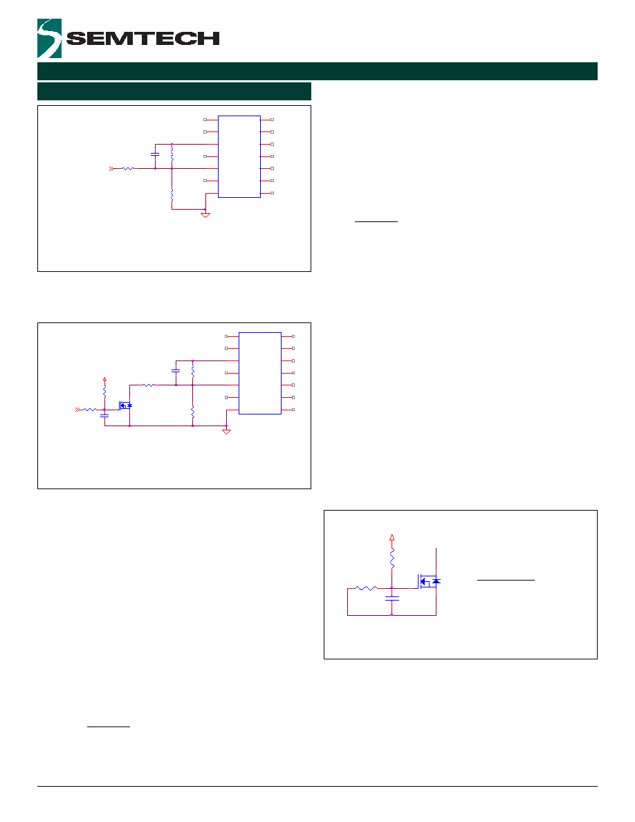
Adding an Additional Output Voltage For Dynamic
Voltage Switching
If we design this output to be capable of dynamically
switching between 1.2V and 1.0V, then we would repeat
these calculations to determine if any components need
changing. The 1.0V output suggests a value for C
TOP
of
82pF, but the value of 56pF required by the 1.2V design
should work fine, and can always be increased if neces-
sary. Also, the current limit resistor required is slightly
higher: R
ILIM
= 7.87k
. The higher value should be used.
Lastly, the bottom feedback resistor, R
BOT
will need to
change to 20.0k
. The schematic in Figure 8 on Page
17 shows the complete design.
Dynamically Switching Output Voltages
It is important to note that in order for dynamic output
voltage switching to work, the SC470 must be in
Continuous Conduction Mode (EN/PSV = floating) when
transitioning from V
OUT(HIGH)
to V
OUT(LOW)
. Otherwise the
SC470 has no means to discharge the output voltage
and may OVP and latch off when this transition is initiated
(depending upon the difference between the two
voltages). If CCM is on, the SC470 will actively discharge
the output down to the correct voltage.
Dynamically switching output voltages is very easy,
requiring one switch to add or remove an additional
resistor in parallel to the bottom feedback resistor. Ideally,
the resistor will be switched using an open drain output
from another IC, as shown in Figure 4.
15
2005 Semtech Corp.
www.semtech.com
SC470
POWER MANAGEMENT
Application Information (Cont.)
Figure 4: Dynamic Voltage Switching Using Direct
Drive Method (V
OUT(HIGH)
/V
OUT(LOW)
< 1.16 only)
Another option is to switch using an external discrete
MOSFET, as shown in Figure 5.
Figure 5: Dynamic Voltage Switching Using Indirect
Drive Method
The problem with the external MOSFET method is that
the drain-gate capacitance, c
DG
, can cause the output
voltage to go even higher when the MOSFET is first turned
off (which should make the output voltage drop). This is
because the gate going low causes the drain to go low
momentarily due to c
DG
, which in turn causes V
FB
to go
low, making the output rise. The extra R9 and C11 in the
gate drive for the MOSFET are there to slow down the
slew rate of the gate voltage, thus avoiding this problem.
Determining what circuit to use depends upon the ratio
between V
OUT(HIGH)
and V
OUT(LOW)
, since the goal is to avoid
inadvertently tripping the over-voltage protection.
If:
16
.
1
V
V
)
LOW
(
OUT
)
HIGH
(
OUT
<
This means that the ratio is less than the worst-case
OVP threshold (worst-case in this case is the lowest
threshold), then the direct drive (simplest) method may
be used. Of course the indirect drive method may also
be used if desired.
If:
16
.
1
V
V
)
LOW
(
OUT
)
HIGH
(
OUT
>
This means that the ratio is greater than the worst-case
OVP threshold, therefore we automatically need to slew
the rate of change, and the indirect drive method must
be used.
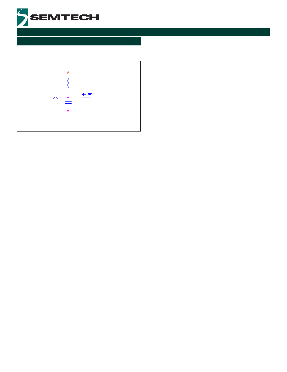
If using the indirect drive method, the goal is to slow
down the gate drive for the transition from V
OUT(HIGH)
to
V
OUT(LOW)
, which is when the external MOSFET is turned
off. The pull-up resistor, pull-down resistor and gate
capacitor can be selected as follows:
1) V
GATE
must be below the gate threshold voltage of the
MOSFET in order to ensure that it can be turned off (see
Figure 6):
2) The RC time constant of R9 and C11 should be at
least 4 times greater than the typical Over-Voltage Fault
Delay Time of 5µs to avoid V
OUT
rising prior to falling.
3) V
PULLUP
must be high enough to turn the MOSFET on.
Figure 6: Ensuring Q3 Will Turn Off
R3
20k0
R7
20k0
EN/PSV
TON
VOUT
VCCA
FB
PGD
VSSA
PGND
DL
VDDP
ILIM
LX
DH
BST
U1
SC470
VOUT
0402
0402
0402
C5
56p
R5 49k9
0402
Low = 1.0V
High = 1.2V
Open Drain Signal
Q3
R8
pull-up
C11
R9
R3
20k0
R7
20k0
EN/PSV
TON
VOUT
VCCA
FB
PGD
VSSA
PGND
DL
VDDP
ILIM
LX
DH
BST
U1
SC470
VOUT
0402
0402
C5
56p
0402
R5 49k9
0402
Open Drain Signal
Low = 1.2V
High = 1.0V
Q3
R8
pull-up
C11
R9
VGATE
VPULLUP
(
)
)
TH
(
GS
PULLUP
V
9
R
8
R
V
9
R
<
+
∑
16
2005 Semtech Corp.
www.semtech.com
SC470
POWER MANAGEMENT
Application Information (Cont.)
Figure 7 below shows recommended components that
work well.
Figure 7: Recommended Component Values
Please see the example switching waveforms on Pages
25 and 26.
Thermal Considerations
The junction temperature of the device may be calculated
as follows:
C
P
T
T
JA
D
A
J
∞
∑
+
=
Where:
T
A
= ambient temperature (∞C)
P
D
= power dissipation in (W)
JA
= thermal impedance junction to ambient from
absolute maximum ratings (∞C/W)
The power dissipation may be calculated as follows:
W
D
mA
1
VBST
f
Q
V
I
VDDP
I
VCCA
P
g
g
VDDP
VCCA
D
∑
∑
+
∑
∑
+
∑
+
∑
=
Where:
VCCA = chip supply voltage (V)
I
VCCA
= operating current (A)
VDDP = gate drive supply voltage (V)
I
VDDP
= gate drive operating current (A)
V
g
= gate drive voltage, typically 5V (V)
Q
g
= FET gate charge, from the FET datasheet (C)
f = switching frequency (kHz)
VBST = boost pin voltage during t
ON
(V)
D = duty cycle
Inserting the following values for VBAT
(MIN)
condition (since
this is the worst-case condition for power dissipation in
the controller) as an example (VOUT = 1.2V):
T
A
= 85∞C
JA
= 100∞C/W (For TSSOP-14)
JA
= 46∞C/W (For MLPQ-16)
VCCA = VDDP = 5V
I
VCCA
= 1100µA (data sheet maximum)
I
VDDP
= 150µA (data sheet maximum)
V
g
= 5V
Q
g
= 60nC
f = 266kHz
VBAT
(MIN)
= 8V
VBST
(MIN)
= VBAT
(MIN)
+VDDP = 13V
D
(MIN)
= 1.2/8 = 0.15
gives us:
W
088
.
0
15
.
0
10
1
13
10
266
10
60
5
10
150
5
10
1100
5
P
3
3
9
6
6
D
=
∑
∑
∑
+
∑
∑
∑
∑
+
∑
∑
+
∑
∑
=
-
-
-
-
So for TSSOP-14,
C
8
.
93
100
088
.
0
85
T
J
∞
=
∑
+
=
And for MLPQ-16,
C
0
.
89
46
088
.
0
85
T
J
∞
=
∑
+
=
As can be seen, the heating effects due to internal power
dissipation are practically negligible, thus requiring no
special consideration thermally during layout.
Q3
R8
10k
C11
22n
R9
1k
VGATE
VPULLUP
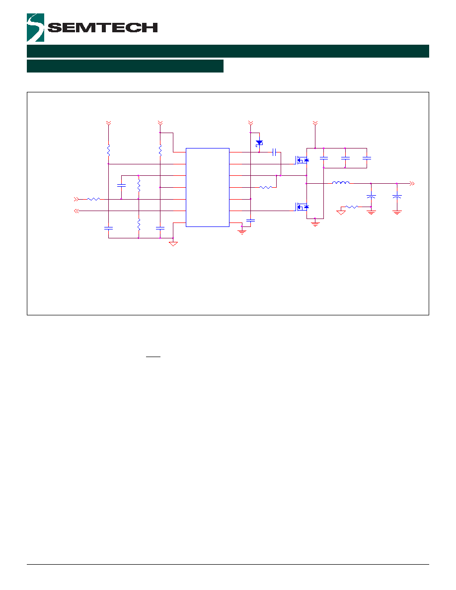
17
2005 Semtech Corp.
www.semtech.com
SC470
POWER MANAGEMENT
Application Information (Cont.)
C10
1uF
R3
20k0
R7
20k0
EN/PSV
1
TON
2
VOUT
3
VCCA
4
FB
5
PGD
6
VSSA
7
PGND
8
DL
9
VDDP
10
ILIM
11
LX
12
DH
13
BST
14
U1
SC470
VOUT
C8
1nF
R1
1M
5VSUS
VBAT
PGOOD
Q1
IRF7811AV
Q2
FDS6676S
C9
1uF
R4 7k87
C1 0.1uF
D1
SOD323
C2
2n2/50V
VBAT
5VSUS
L1
2u2
+
C7
220u/25m
VOUT
R2
10R
0402
0402
0402
0402
C5
56p
0402
R5 49k9
0402
VOUT SWITCH (1)
0402
0603
R6 0R (2)
0402
7343
+
C6
220u/25m
7343
0402
C3
0u1/25V
C4
10u/25V
0603
1210
0603
0402
0603
N OTES
(1) driv en by an open drain with no pullup. LOW = 1.2V out, FLOATIN G = 1V out.
(2) R 6 is not required but aids keeping VSSA s eparate f rom PGN D ex c ept where des ired in lay out.
VBAT = 8V to 20V
VOUT = 1.2V or 1.0V @ 6A
Figure 8: Reference Design For Dynamic Output Switching
One (or more) ground planes is/are recommended to minimize the effect of switching noise and copper losses, and
maximize heat dissipation. The IC ground reference, VSSA, should be kept separate from power ground. All
components that are referenced to VSSA should connected to it locally at the chip. VSSA should connect to power
ground at the output capacitor(s) only.
The VOUT feedback trace must be kept far away from noise sources such as switching nodes, inductors and gate
drives. Route the feedback trace with VSSA as a differential pair from the output capacitor back to the chip. Run
them in a "quiet layer" if possible. VSSA may be separated from PGND using a zero Ohm resistor (that will be placed
at the bottom of the output capacitors) to aid in net separation.
Chip decoupling capacitors (VDDP, VCCA) should be located next to the pins (VDDP and PGND, VCCA and VSSA) and
connected directly to them on the same side.
Power sections should connect directly to the ground plane(s) using multiple vias as required for current handling
(including the chip power ground connections). Power components should be placed to minimize loops and reduce
losses. Make all the connections on one side of the PCB using wide copper filled areas if possible. Do not use
"minimum" land patterns for power components. Minimize trace lengths between the gate drivers and the gates of
the MOSFETs to reduce parasitic impedances (and MOSFET switching losses), the low-side MOSFET is most critical.
Maintain a length to width ratio of <20:1 for gate drive signals. Use multiple vias as required by current handling
requirement (and to reduce parasitics) if routed on more than one layer
Current sense connections must always be made using Kelvin connections to ensure an accurate signal, with the
current limit resistor located at the device.
We will examine the reference design used in the Design Procedure section while explaining the layout guidelines in
more detail.
Layout Guidelines - TSSOP-14 as an example:
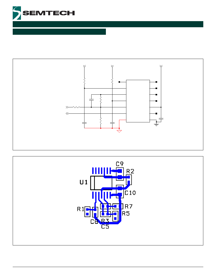
18
2005 Semtech Corp.
www.semtech.com
SC470
POWER MANAGEMENT
The layout can be considered in two parts, the control section referenced to VSSA and the power section. Looking
at the control section first, locate all components referenced to VSSA on the schematic and place these components
at the chip. Connect VSSA using either a wide (>0.020") trace or a copper pour if room allows. Very little current
flows in the chip ground therefore large areas of copper are not needed.
C10
1uF
R3
20k0
R7
20k0
EN/PSV
1
TON
2
VOUT
3
VCCA
4
FB
5
PGD
6
VSSA
7
PGND
8
DL
9
VDDP
10
ILIM
11
LX
12
DH
13
BST
14
U1
SC470
VOUT
C8
1nF
R1
1M
5VSUS
PGOOD
VBAT
C9
1uF
5VSUS
R2
10R
0402
0402
0402
0402
C5
56p
0402
R5 49k9
0402
VOUT SWITCH (1)
0603
0402
0603
Figure 9: Components Connected to VSSA
Figure 10: Example VSSA 0.020" Traces
Application Information (Cont.)
In Figure 10 above, all components referenced to VSSA have been placed and have been connected using 0.020"
traces. Decoupling capacitors C9 and C10 are as close as possible to their pins. C9 should connect to the ground
plane using two vias
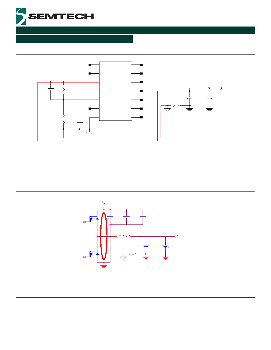
19
2005 Semtech Corp.
www.semtech.com
SC470
POWER MANAGEMENT
As shown below, VOUT and VSSA should be routed as a differential pair to the output capacitor(s).
C11
1uF
R4
20k0
R8
20k0
EN/PSV
1
TON
2
VOUT
3
VCCA
4
FB
5
PGD
6
VSSA
7
PGND
8
DL
9
VDDP
10
ILIM
11
LX
12
DH
13
BST
14
U2
SC470
VOUT
+
C7
220u/25m
VOUT
0402
0402
C6
56p
0402
0603
R12 0R (2)
7343
0402
+
C14
220u/25m
7343
VOUT
VOUT
VSSA
Figure 11: Differential Routing of Feedback and Ground Reference Traces
Next, the schematic in Figure 12 below shows the power section. The highest di/dts occur in the input loop (highlighted
in red) and thus this loop should be kept as small as possible.
Q1
IRF7811AV
Q2
FDS6676S
C2
2n2/50V
VBAT
L1
2u2
+
C7
220u/25m
VOUT
R6 0R (2)
7343
0402
+
C6
220u/25m
7343
0402
C3
0u1/25V
C4
10u/25V
1210
0603
Figure 12: Power Section and Input Loop
The input capacitors should be placed with the highest frequency capacitors closest to the loop to reduce EMI. Use
large copper pours to minimize losses and parasitics. See Figure 13 on Page 20 for an example.
Application Information (Cont.)
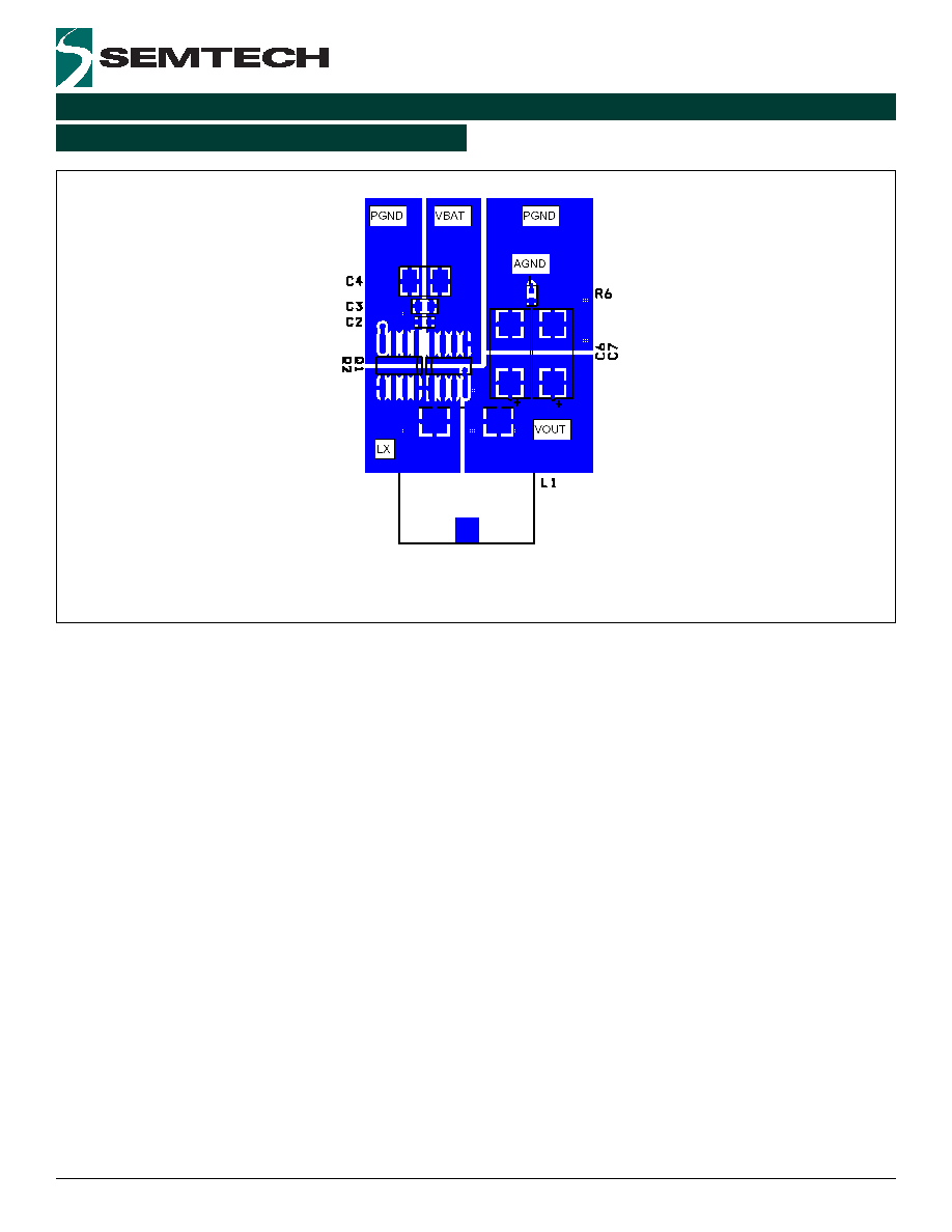
20
2005 Semtech Corp.
www.semtech.com
SC470
POWER MANAGEMENT
Application Information (Cont.)
Figure 13: Power Component Placement and Copper Pours
Key points for the power section:
1) There should be a very small input loop, well decoupled.
2) The phase node should be a large copper pour, but compact since this is the noisiest node.
3) Input power ground and output power ground should not connect directly, but through the ground planes instead.
4) Notice in Figure 10 on page 18, the placement of 0
resistor at the bottom of the output capacitor to connect
to VSSA.
5) The current limit resistor should be placed as close as possible to the ILIM and LX pins.
Connecting the control and power sections should be accomplished as follows (see Figure 14 on Page 21):
1) Route VSSA and VOUT as differential pairs routed in a "quiet" layer away from noise sources.
2) Route DL, DH and LX (low-side FET gate drive, high side FET gate drive and phase node) to chip using wide traces
with multiple vias if using more than one layer. These connections to be as short as possible for loop minimization,
with a length to width ratio less than 20:1 to minimize impedance. DL is the most critical gate drive, with power
ground as its return path. LX is the noisiest node in the circuit, switching between V
BAT
and ground at high frequencies,
thus should be kept as short as practical. DH has LX as its return path.
3) BST is also a noisy node and should be kept as short as possible.
4) Connect PGND pin on the chip directly to the VDDP decoupling capacitor and then drop vias directly to the ground
plane.
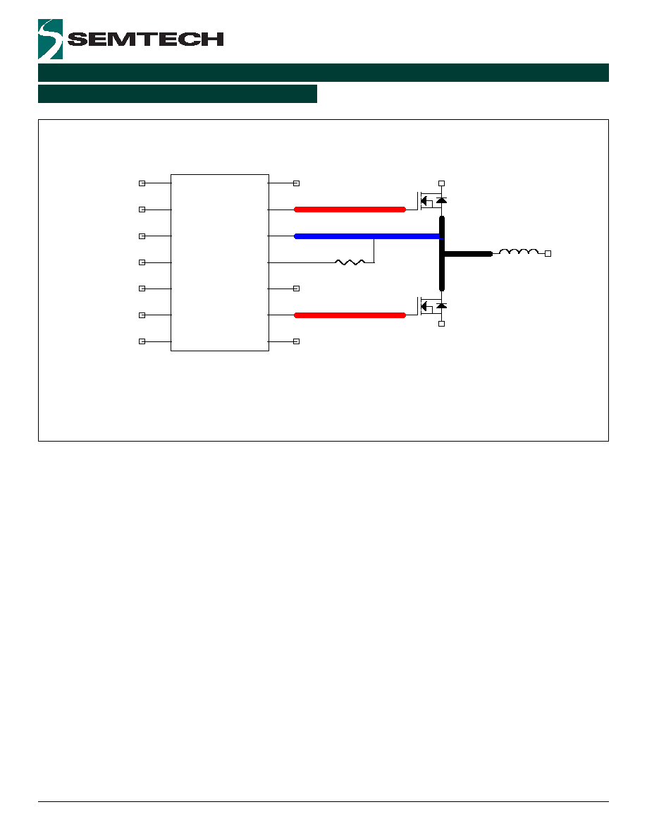
21
2005 Semtech Corp.
www.semtech.com
SC470
POWER MANAGEMENT
Figure 14: Connecting The Control and Power Sections
Application Information (Cont.)
EN/PSV
1
TON
2
VOUT
3
VCCA
4
FB
5
PGD
6
VSSA
7
PGND
8
DL
9
VDDP
10
ILIM
11
LX
12
DH
13
BST
14
U1
SC470
Q1
IRF7811AV
Q2
FDS6676S
R4 7k87
L1
2u2
0402
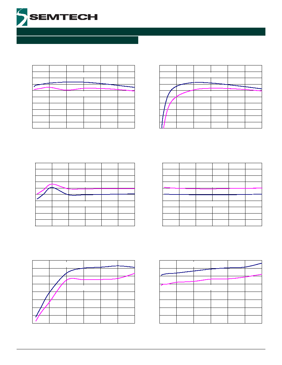
22
2005 Semtech Corp.
www.semtech.com
SC470
POWER MANAGEMENT
Typical Characteristics
1.2V Efficiency (Power Save Mode)
vs. Output Current vs. Input Voltage
1.2V Efficiency (Continuous Conduction Mode)
vs. Output Current vs. Input Voltage
1.2V Output Voltage (Power Save Mode)
vs. Output Current vs. Input Voltage
1.2V Output Voltage (Continuous Conduction Mode)
vs. Output Current vs. Input Voltage
1.2V Switching Frequency (Power Save Mode)
vs. Output Current vs. Input Voltage
1.2V Switching Frequency (Continuous Conduction
Mode) vs. Output Current vs. Input Voltage
50
55
60
65
70
75
80
85
90
95
100
0
1
2
3
4
5
6
I
OUT
(A)
E
ffi
cien
cy (
%
)
V
BAT
= 20V
V
BAT
= 8V
1.180
1.184
1.188
1.192
1.196
1.200
1.204
1.208
1.212
1.216
1.220
0
1
2
3
4
5
6
I
OUT
(A)
V
OUT
(V
)
V
BAT
= 20V
V
BAT
= 8V
0
50
100
150
200
250
300
350
400
0
1
2
3
4
5
6
I
OUT
(A)
F
r
eq
ue
ncy (kH
z
)
V
BAT
= 20V
V
BAT
= 8V
50
55
60
65
70
75
80
85
90
95
100
0
1
2
3
4
5
6
I
OUT
(A)
E
ffi
cien
cy (
%
)
V
BAT
= 8V
V
BAT
= 20V
1.180
1.184
1.188
1.192
1.196
1.200
1.204
1.208
1.212
1.216
1.220
0
1
2
3
4
5
6
I
OUT
(A)
V
OUT
(V
)
V
BAT
= 20V
V
BAT
= 8V
0
50
100
150
200
250
300
350
400
0
1
2
3
4
5
6
I
OUT
(A)
F
r
eq
ue
ncy (kH
z
)
V
BAT
= 20V
V
BAT
= 8V
Please refer to Figure 8 on Page 17 for test schematic
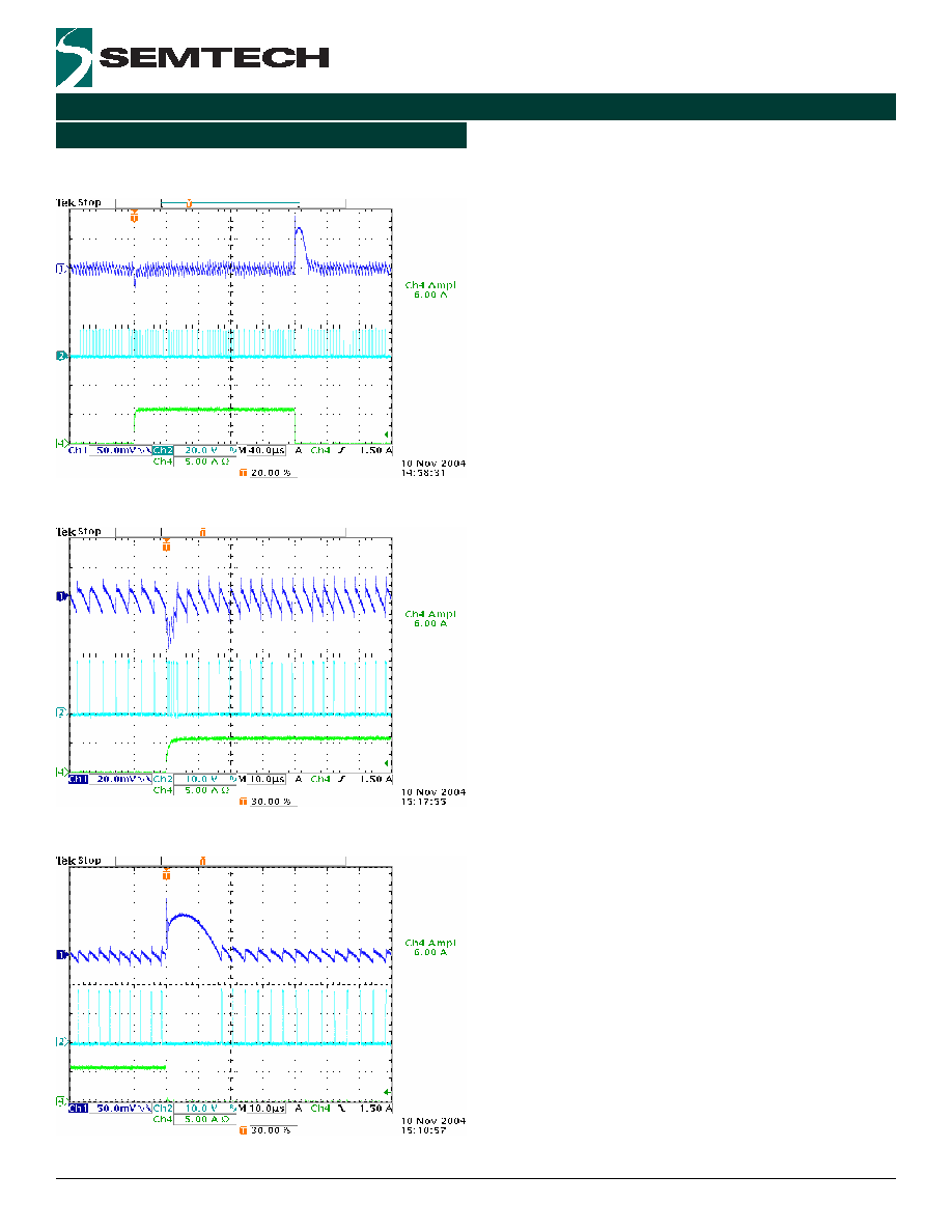
23
2005 Semtech Corp.
www.semtech.com
SC470
POWER MANAGEMENT
Typical Characteristics (Cont.)
Load Transient Response,
Continuous Conduction Mode, 0A to 6A to 0A
Trace 1: 1.2V, 50mV/div., AC coupled
Trace 2: LX, 20V/div
Trace 3: not connected
Trace 4: load current, 5A/div
Timebase: 40µs/div.
Load Transient Response,
Continuous Conduction Mode, 0A to 6A Zoomed
Load Transient Response,
Continuous Conduction Mode, 6A to 0A Zoomed
Trace 1: 1.2V, 50mV/div., AC coupled
Trace 2: LX, 10V/div
Trace 3: not connected
Trace 4: load current, 5A/div
Timebase: 10µs/div.
Trace 1: 1.2V, 20mV/div., AC coupled
Trace 2: LX, 10V/div
Trace 3: not connected
Trace 4: load current, 5A/div
Timebase: 10µs/div.
Please refer to Figure 8 on Page 17 for test schematic
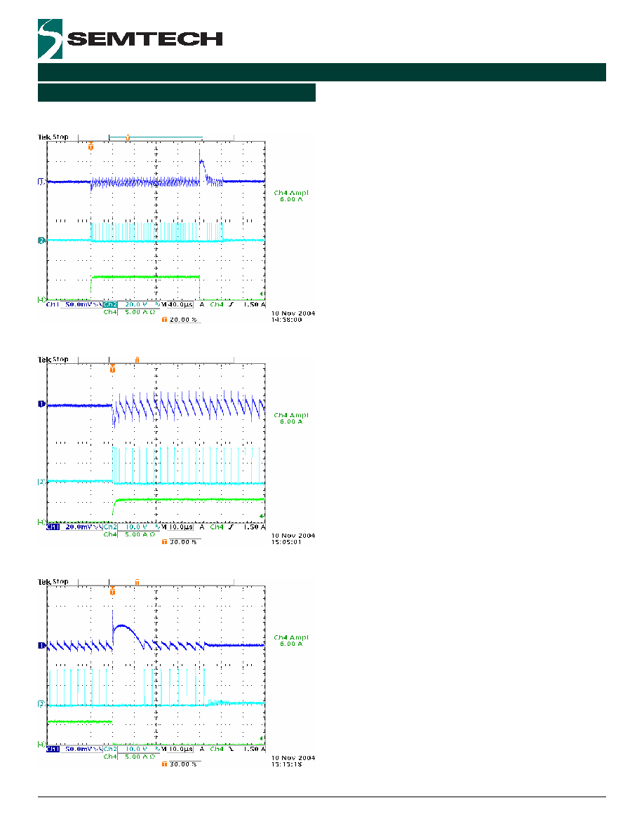
24
2005 Semtech Corp.
www.semtech.com
SC470
POWER MANAGEMENT
Typical Characteristics (Cont.)
Load Transient Response,
Power Save Mode, 0A to 6A to 0A
Trace 1: 1.2V, 50mV/div., AC coupled
Trace 2: LX, 20V/div
Trace 3: not connected
Trace 4: load current, 5A/div
Timebase: 40µs/div.
Load Transient Response,
Power Save Mode, 0A to 6A Zoomed
Load Transient Response,
Power Save Mode, 6A to 0A Zoomed
Trace 1: 1.2V, 50mV/div., AC coupled
Trace 2: LX, 10V/div
Trace 3: not connected
Trace 4: load current, 5A/div
Timebase: 10µs/div.
Trace 1: 1.2V, 20mV/div., AC coupled
Trace 2: LX, 10V/div
Trace 3: not connected
Trace 4: load current, 5A/div
Timebase: 10µs/div.
Please refer to Figure 8 on Page 17 for test schematic
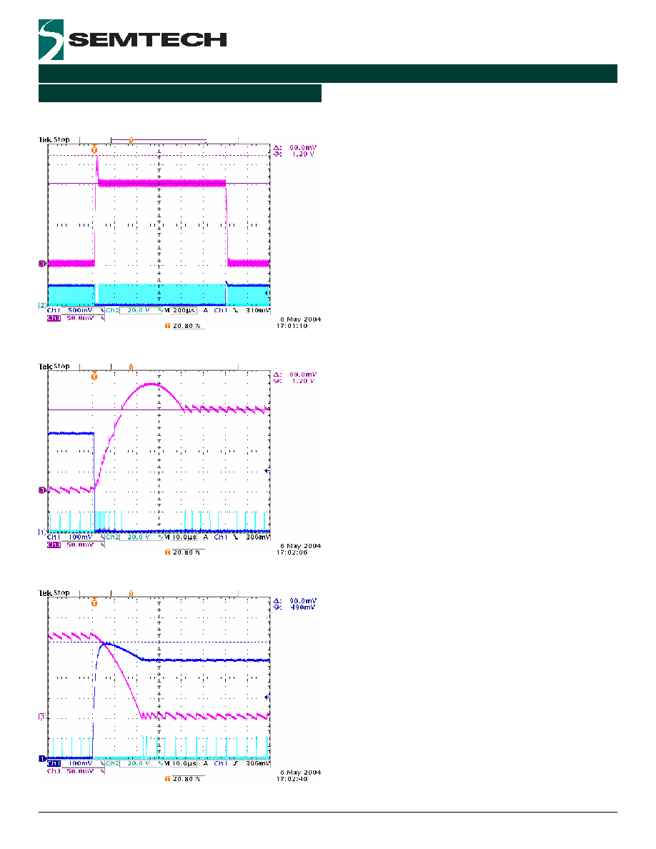
25
2005 Semtech Corp.
www.semtech.com
SC470
POWER MANAGEMENT
Typical Characteristics (Cont.)
Dynamic Output Voltage Switching
From 1V to 1.2V to 1V, No Load
Trace 1: toggle signal (for reference only)
Trace 2: LX, 20V/div
Trace 3: VOUT, 50mV/div, offset 1V
Trace 4: not connected
Timebase: 200µs/div.
Dynamic Output Voltage Switching
From 1V to 1.2V Zoomed, No Load
Dynamic Output Voltage Switching
From 1.2V to 1V Zoomed, No Load
Trace 1: toggle signal (for reference only)
Trace 2: LX, 20V/div
Trace 3: VOUT, 50mV/div, offset 1V
Trace 4: not connected
Timebase: 10µs/div.
Trace 1: toggle signal (for reference only)
Trace 2: LX, 20V/div
Trace 3: VOUT, 50mV/div, offset 1V
Trace 4: not connected
Timebase: 10µs/div.
Please refer to Figure 8 on Page 17 for test schematic
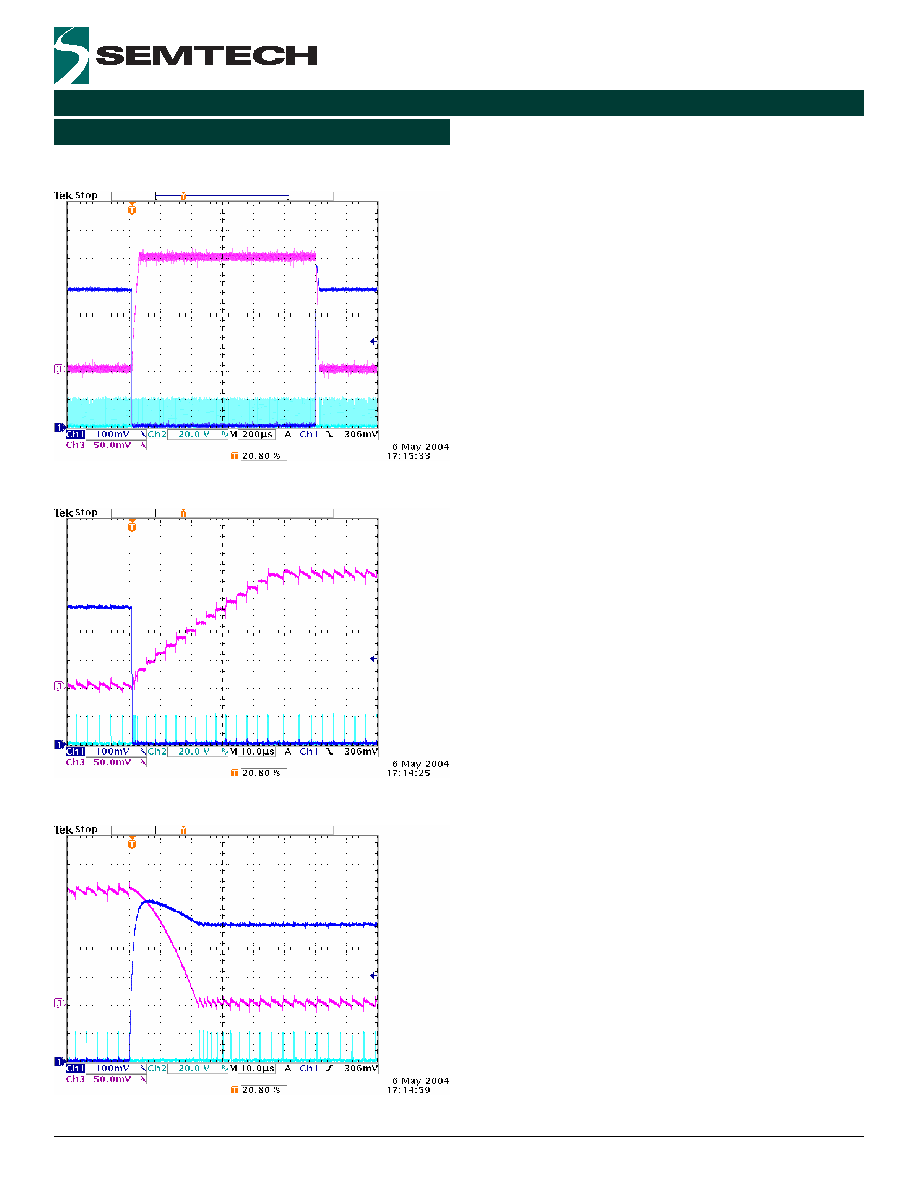
26
2005 Semtech Corp.
www.semtech.com
SC470
POWER MANAGEMENT
Typical Characteristics (Cont.)
Dynamic Output Voltage Switching
From 1V to 1.2V to 1V, 6A Load
Trace 1: toggle signal (for reference only)
Trace 2: LX, 20V/div
Trace 3: VOUT, 50mV/div, offset 1V
Trace 4: not connected
Timebase: 200µs/div.
Dynamic Output Voltage Switching
From 1V to 1.2V Zoomed, 6A Load
Dynamic Output Voltage Switching
From 1.2V to 1V Zoomed, 6A Load
Trace 1: toggle signal (for reference only)
Trace 2: LX, 20V/div
Trace 3: VOUT, 50mV/div, offset 1V
Trace 4: not connected
Timebase: 10µs/div.
Trace 1: toggle signal (for reference only)
Trace 2: LX, 20V/div
Trace 3: VOUT, 50mV/div, offset 1V
Trace 4: not connected
Timebase: 10µs/div.
Please refer to Figure 8 on Page 17 for test schematic
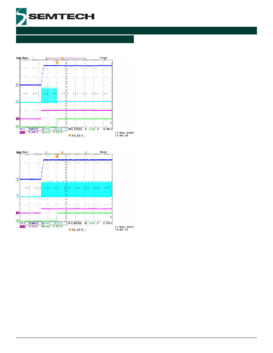
27
2005 Semtech Corp.
www.semtech.com
SC470
POWER MANAGEMENT
Typical Characteristics (Cont.)
Startup (PSV), EN/PSV Going High
Trace 1: 1.2V, 0.5V/div.
Trace 2: LX, 10V/div
Trace 3: EN/PSV, 5V/div
Trace 4: PGD, 5V/div.
Timebase: 1ms/div.
Startup (CCM), EN/PSV 0V to Floating
Trace 1: 1.2V, 0.5V/div.
Trace 2: LX, 10V/div
Trace 3: EN/PSV, 5V/div
Trace 4: PGD, 5V/div.
Timebase: 1ms/div.
Please refer to Figure 8 on Page 17 for test schematic
28
2005 Semtech Corp.
www.semtech.com
SC470
POWER MANAGEMENT
Marking Information - MLPQ-16
Outline Drawing - MLPQ-16
INDICATOR
(LASER MARK)
PIN 1
DIMENSIONS
NOM
INCHES
N
bbb
aaa
A2
A1
E1
D1
DIM
L
e
E
D
A
b
MIN
MAX
MILLIMETERS
MIN
MAX
NOM
.153
.157
.161
3.90
4.00
4.10
.153
.157
.161
3.90
4.00
4.10
E1
.003
.010
.079
16
.012
.085
-
.000
.031
(.008)
0.08
0.30
16
.014
.089
0.25
2.00
.040
-
.002
-
0.00
0.80
2.25
0.35
2.15
-
0.05
1.00
(0.20)
.004
0.10
2.00
2.15
2.25
0.65 BSC
.026 BSC
0.30
.012
.020
.016
0.40
0.50
.089
.085
.079
D/2
2
A
A1
1
LxN
bbb
C A B
A2
bxN
e
SEATING
PLANE
C
E/2
D1
N
e/2
aaa C
CONTROLLING DIMENSIONS ARE IN MILLIMETERS (ANGLES IN DEGREES).
COPLANARITY APPLIES TO THE EXPOSED PAD AS WELL AS THE TERMINALS.
1.
2.
NOTES:
A
D
E
B
-
-
-
-
Marking for the 4 x 4mm MLPQ 16 Lead package:
yyww
nnnnn = Part Number (Example: SC470)
yyww = Date Code (Example: 0552)
xxxxx = Semtech Lot No. (Example: E9010
xxxxx 1-100)
xxxxx
xxxxx
SC470
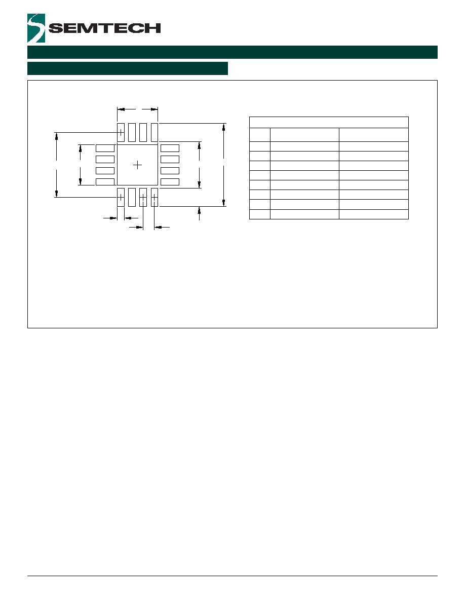
29
2005 Semtech Corp.
www.semtech.com
SC470
POWER MANAGEMENT
Land Pattern - MLPQ-16
THIS LAND PATTERN IS FOR REFERENCE PURPOSES ONLY.
CONSULT YOUR MANUFACTURING GROUP TO ENSURE YOUR
COMPANY'S MANUFACTURING GUIDELINES ARE MET.
NOTES:
1.
2x G
H
2x (C)
2x Z
X
P
Y
K
C
Z
P
Y
X
G
K
H
.189
.026
.016
.037
.114
.091
.091
4.80
0.40
0.95
0.65
2.30
2.30
2.90
DIM
(3.85)
MILLIMETERS
DIMENSIONS
(.152)
INCHES
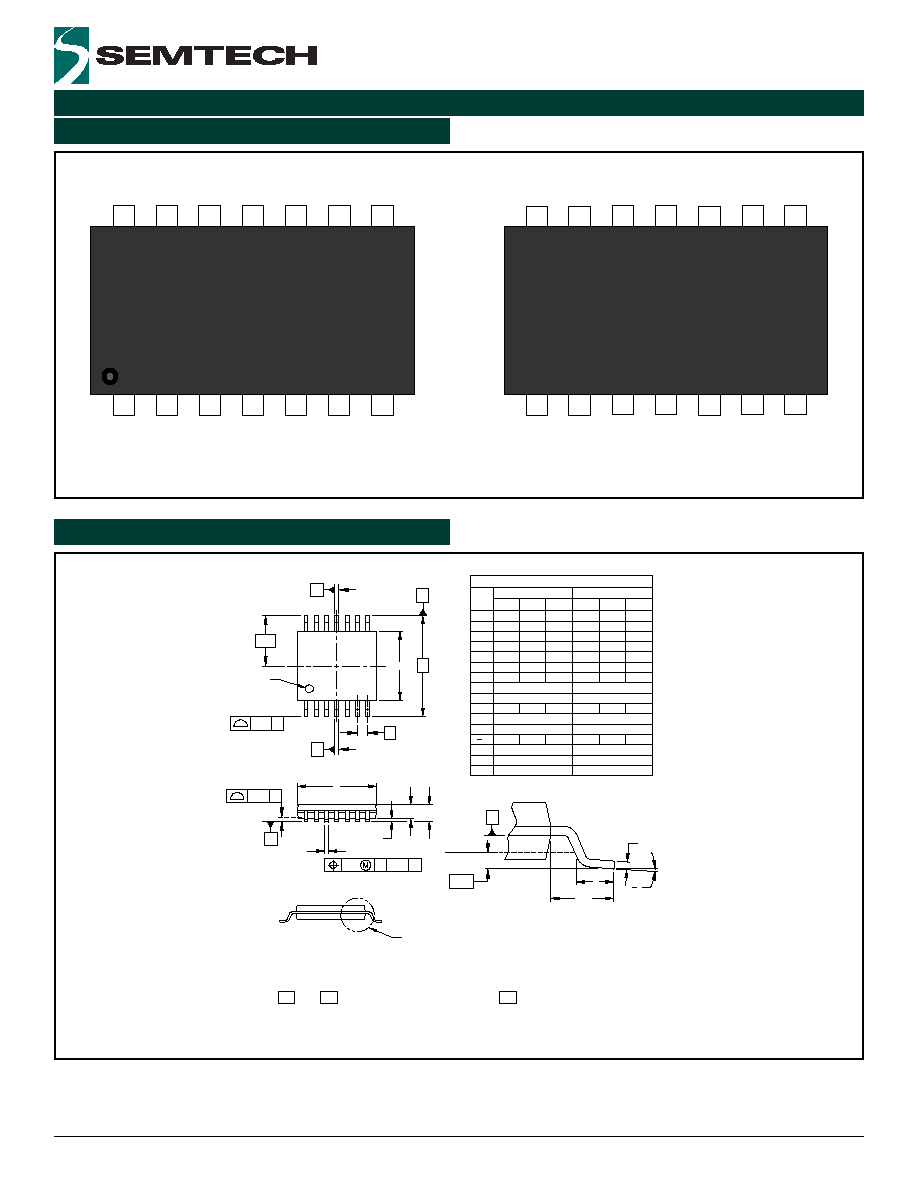
30
2005 Semtech Corp.
www.semtech.com
SC470
POWER MANAGEMENT
Outline Drawing - TSSOP-14
Marking Information - TSSOP-14
Top Mark
Bottom
yyww = Datecode (Example: 9812)
xxxxxx = Semtech Lot # (Example: 81101)
SC470I
xxxxxx
yyww
NOM
INCHES
DIMENSIONS
c
N
ccc
aaa
bbb
01
E
L1
L
e
E1
D
MIN
A
A1
A2
b
DIM
MILLIMETERS
MIN
MAX
NOM MAX
E
REFERENCE JEDEC STD MO-153, VARIATION AB-1.
4.
GAGE
PLANE
SEE DETAIL
DETAIL
A
A
0.25
.026 BSC
.252 BSC
14
.004
.169
.193
.173
.197
.007
-
14
0.10
0.65 BSC
6.40 BSC
4.40
5.00
-
.177
.201
4.30
4.90
.012 0.19
4.50
5.10
0.30
PIN 1
INDICATOR
SEATING
bbb
C A-B D
ccc C
PLANE
DIMENSIONS "E1" AND "D" DO NOT INCLUDE MOLD FLASH, PROTRUSIONS
3.
OR GATE BURRS.
DATUMS AND TO BE DETERMINED AT DATUM PLANE
CONTROLLING DIMENSIONS ARE IN MILLIMETERS (ANGLES IN DEGREES).
-B-
NOTES:
1.
2.
-A-
-H-
SIDE VIEW
A
B
C
D
e
H
D
0∞
.008
-
.004
.018
.003
(.039)
.024
-
.031
.002
-
-
-
-
0.10
0.20
8∞
0∞
-
8∞
0.60
(1.0)
.030
.007
0.45
0.09
.047
.042
.006
0.80
0.05
-
0.20
0.75
-
1.05
0.15
1.20
-
-
-
bxN
A
A2
A1
E/2
2X
E1
2X N/2 TIPS
1 2 3
aaa C
L
(L1)
c
01
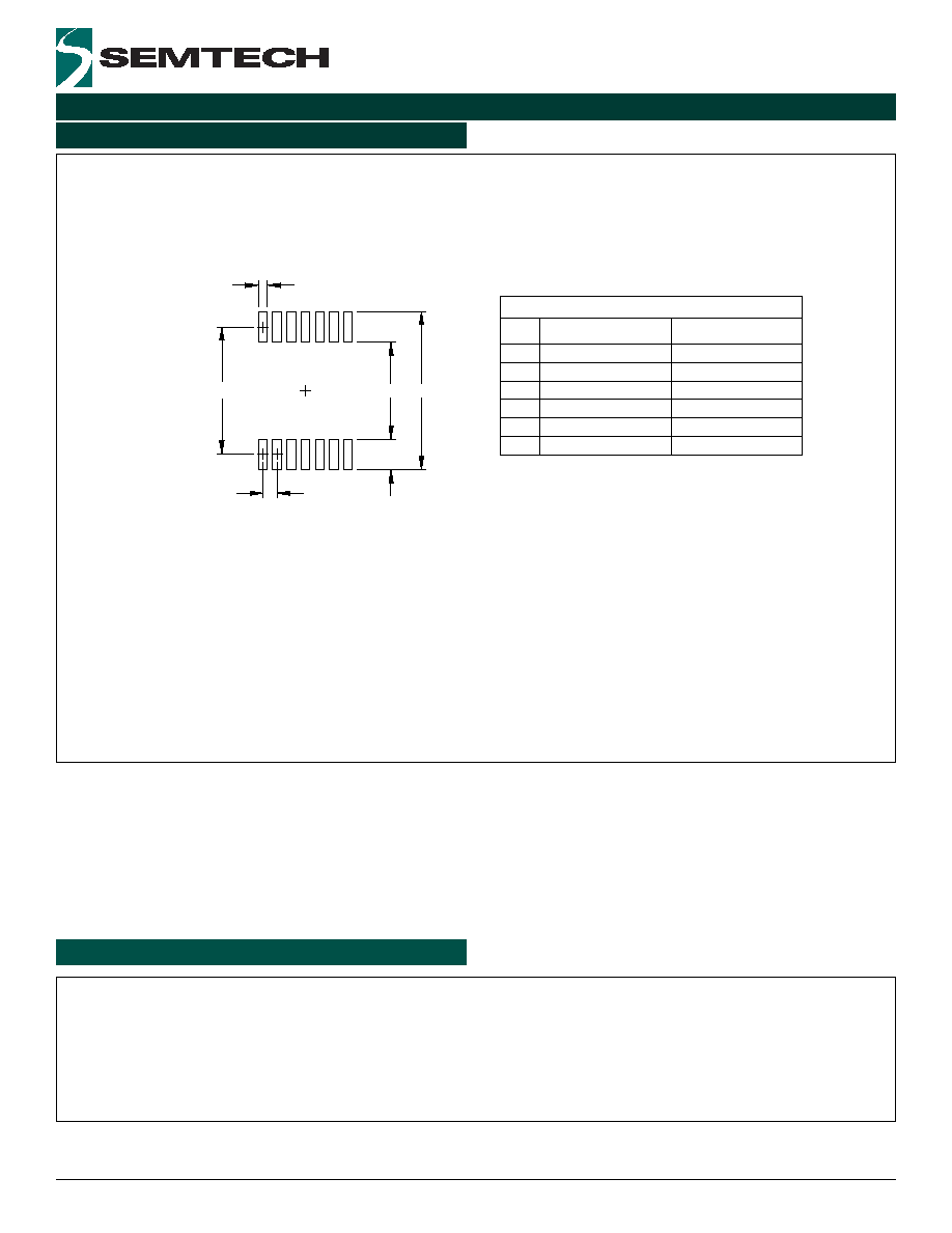
31
2005 Semtech Corp.
www.semtech.com
SC470
POWER MANAGEMENT
Land Pattern - TSSOP-14
(.222)
(5.65)
Z
G
Y
P
(C)
4.10
.161
0.65
.026
0.40
.016
1.55
.061
7.20
.283
X
INCHES
DIMENSIONS
Z
P
Y
X
DIM
C
G
MILLIMETERS
THIS LAND PATTERN IS FOR REFERENCE PURPOSES ONLY.
CONSULT YOUR MANUFACTURING GROUP TO ENSURE YOUR
COMPANY'S MANUFACTURING GUIDELINES ARE MET.
NOTES:
1.
Visit us at:
www.semtech.com
Semtech Corporation
Power Management Products Division
200 Flynn Road, Camarillo, CA 93012
Phone: (805) 498-2111 FAX (805)498-3804
Contact Information