1
www.semtech.com
SC4806
Multiple Function
Double Ended PWM Controller
POWER MANAGEMENT
Revision: July 13, 2005
Description
Features
Applications
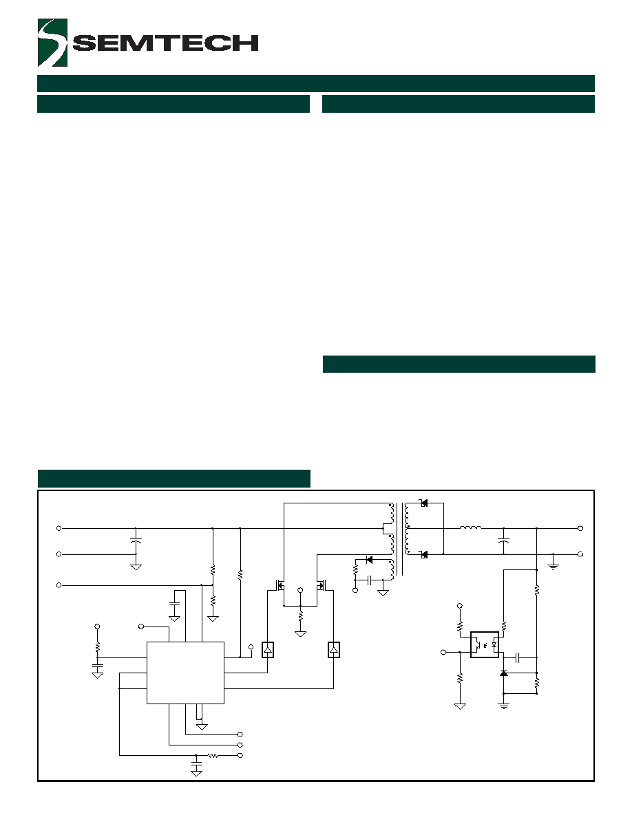
Typical Application Circuit
90 µA starting current
Pulse-by-pulse current limit for both voltage/current
modes
Programmable operating frequency up to 1MHz
Programmable external soft start
Programmable line undervoltage lockout
Programmable external slope compensation
Over current shutdown with separate pin
Dual output drive stages on push-pull configuration
Programmable mode of operation (peak current mode
or voltage mode)
External frequency synchronization
Bi-phase mode of operation
Lead free MLP-12 package,WEEE and RoHS
compliant
-40 to 105 °C operating temperature
Telecom equipment and power supplies
Networking power supplies
Industrial power supplies
Push-pull converter
Half bridge converter
Full bridge converter
Isolated VRMs
The SC4806 is a double ended, high speed, highly
integrated PWM controller optimized for applications
requiring minimum space. The device is easily configurable
for current mode or voltage mode operation and contains
all the control circuitry required for isolated applications,
where a secondary side error amplifier is used.
Designed for simplicity, the SC4806 is fully featured and
requires only a few external components. It features a
programmable frequency up to 1MHZ, external
programmable soft start, pulse-by-pulse current limit and
over current protection for both voltage and current
modes, as well as a line monitoring input with hysteresis
to reduce stress on the power components. A ramp pin
allows for slope compensation to be programmed by
external resistors for current mode. This also allows for
operation in voltage mode with voltage feed forward.
A unique oscillator is utilized which allows two SC4806
to be synchronized together and work out-of-phase. This
feature minimizes the input and output ripples, and
reduces stress and size on input/output filter components.
The outputs are configured for push-pull format, dead time
between the 2 outputs is programmable depending on the
size of the timing components.
The SC4806 features a turn on threshold of 8 volts .
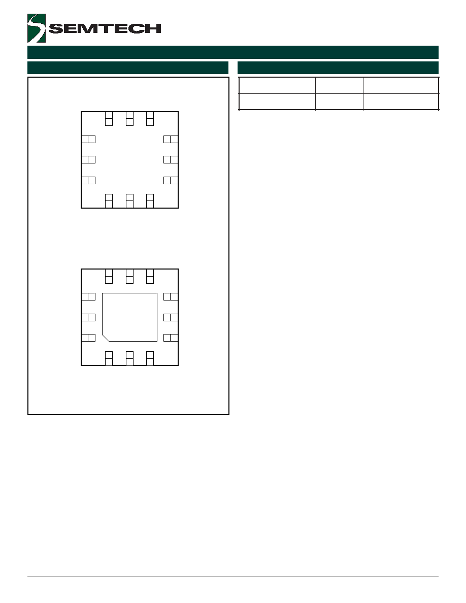
The device is available at a MLP-12 package.
Vcc
+VIN
SYNC
ON/OFF
-VIN
+
SC431
I sense
+Vo
Rsense
REF
GN
D
9
ILIM
5
OUTB
10
FB
7
LU
V
L
O
1
VCC
12
SS
2
SY
N
C
3
RC
4
RE
F
8
RAMP
6
OUTA
11
GN
D
(
he
at
s
i
nk
)
0
SC4806
I sense
-Vo
SC1301A
FB
SC1301A
FB
+
REF
Vcc
REF
2
2005 Semtech Corp.
www.semtech.com
SC4806
POWER MANAGEMENT
Absolute Maximum Ratings
Electrical Characteristics
r
e
t
e
m
a
r
a
P
s
n
o
i
t
i
d
n
o
C
t
s
e
T
n
i
M
p
y
T
x
a
M
s
t
i
n
U
y
l
p
p
u
S
C
C
V
V
C
C
d
l
o
h
s
e
r
h
T
t
r
a
t
S
4
.
7
8
6
.
8
V
s
i
s
e
r
e
t
s
y
H
7
1
.
1
5
.
1
3
8
.
1
V
t
n
e
r
r
u
C
p
u
t
r
a
t
S
d
l
o
h
s
e
r
h
t
t
r
a
t
s
<
C
C
V
0
5
1
A
µ
t
n
e
r
r
u
C
y
l
p
p
u
S
g
n
it
a
r
e
p
O
V
0
=
P
M
A
R
,
V
0
=
B
F
7
A
m
e
g
a
tl
o
V
t
n
u
h
S
r
e
n
e
Z
C
C
V
A
m
0
1
=
D
D
I
6
1
V
M
W
P
e
l
c
y
C
y
t
u
D
m
u
m
i
x
a
M
,
V
5
=
B
F
,
z
H
k
0
5
=
c
s
o
F
B
T
U
O
r
o
A
T
U
O
t
a
d
e
r
u
s
a
e
M
8
4
9
4
0
5
%
e
l
c
y
C
y
t
u
D
m
u
m
i
n
i
M
,
V
5
.
1
=
B
F
,
z
H
k
0
5
=
c
s
o
F
B
T
U
O
r
o
A
T
U
O
t
a
d
e
r
u
s
a
e
M
0
%
t
i
m
i
L
/
e
s
n
e
S
t
n
e
r
r
u
C
d
l
o
h
s
e
r
h
T
ti
m
i
L
t
n
e
r
r
u
C
e
l
c
y
C
y
b
e
l
c
y
C
M
L
I
0
5
4
5
2
5
0
0
6
V
m
y
a
l
e
D
t
u
p
t
u
O
o
t
M
L
I
0
5
s
n
d
l
o
h
s
e
r
h
T
t
n
e
r
r
u
C
r
e
v
O
t
r
a
t
s
e
R
o
t
u
A
M
L
I
0
5
7
0
5
8
0
5
9
V
m
t
e
s
ff
O
P
M
A
R
o
t
B
F
0
2
.
1
0
4
.
1
0
6
.
1
V
r
e
t
e
m
a
r
a
P
l
o
b
m
y
S
m
u
m
i
x
a
M
s
t
i
n
U
e
g
a
tl
o
V
y
l
p
p
u
S
V
C
C
8
1
o
t
5
.
0
-
V
t
n
e
r
r
u
C
y
l
p
p
u
S
I
C
C
0
2
A
m
D
N
G
o
t
S
S
,
M
L
I
,
F
E
R
,
O
L
V
U
L
,
P
M
A
R
,
C
R
,
C
N
Y
S
7
o
t
5
.
0
-
V
D
N
G
o
t
B
F
V
B
F
V
(
o
t
5
.
0
-
F
E
R
)
5
.
0
+
V
t
n
e
r
r
u
C
F
E
R
I
F
E
R
0
1
A
m
D
N
G
o
t
B
T
U
O
/
A
T
U
O
V
B
/
A
T
U
O
8
1
o
t
5
.
0
-
V
)
k
a
e
p
(
t
n
e
r
r
u
C
e
c
r
u
o
S
B
T
U
O
/
A
T
U
O
I
e
c
r
u
o
s
0
5
2
-
A
m
)
k
a
e
p
(
t
n
e
r
r
u
C
k
n
i
S
B
T
U
O
/
A
T
U
O
I
k
n
i
s
0
5
2
A
m
t
n
e
i
b
m
A
o
t
n
o
it
c
n
u
J
,
e
c
n
a
t
s
i
s
e
R
l
a
m
r
e
h
T
A
J
8
4
W
/
C
°
e
s
a
C
o
t
n
o
it
c
n
u
J
,
e
c
n
a
t
s
i
s
e
R
l
a
m
r
e
h
T
C
J
3
W
/
C
°
e
r
u
t
a
r
e
p
m
e
T
n
o
it
c
n
u
J
T
J
0
5
1
o
t
5
5
-
C
°
e
g
n
a
R
e
r
u
t
a
r
e
p
m
e
T
e
g
a
r
o
t
S
T
G
T
S
0
5
1
o
t
5
6
-
C
°
s
0
4
-
0
1
e
r
u
t
a
r
e
p
m
e
T
w
o
lf
e
R
R
I
k
a
e
P
T
G
K
P
0
6
2
C
°
)l
e
d
o
M
y
d
o
B
n
a
m
u
H
(
g
n
it
a
R
D
S
E
D
S
E
2
V
k
Unless specified: VCC = 12V; CL = 100pF; T
A
= -40°C to 105°C
Exceeding the specifications below may result in permanent damage to the device, or device malfunction. Operation outside of the parameters specified in
the Electrical Characteristics section is not implied.
45455

5
2005 Semtech Corp.
www.semtech.com
SC4806
POWER MANAGEMENT
Pin Descriptions
LUVLO (Pin 1):
Line undervoltage lockout pin. An external resistive di-
vider from the Input supply will program the undervoltage
lockout level. The external divider should be referenced
to the quiet analog ground. During the LUVLO, the driver
outputs are disabled. This pin can also function as an
Enable/Disable.
SS (Pin 2):
An internal 35µA current source charges the external
capacitor connected to this pin. This pin is connected to
one of the inputs of the PWM comparator. When the volt-
age on this SS pin increases, but less than 1/3 of the
feedback voltage V
FB
, the pulse width of OUTA and OUTB
gradually increases to achieve soft start. As the output
voltage increases and feedback loop enters regulation,
the PWM modulator is controlled by V
FB
. At normal opera-
tion, the voltage at SS pin is clamped at Vref.
When the Over Current is tripped, both OUTA and OUTB
are pulled low after a typical time delay (Typ. 100ns). At
the same time, the SS cap is gradually discharged via an
equivalent 10µA internal current source. When the volt-
age on SS pin is dropped below 0.8V, a new SS cycle is
initiated while the SS cap is charged with 35µA again.
The internal thermal protection circuit monitors the die
temperature. If the temperature exceeds 175
o
C, the con-
troller is completely shutdown. When the temperature is
dropped below 160
o
C, defined by the hysteresis, the con-
troller re-starts with soft start process.
SYNC (Pin 3):
SYNC is a positive edge triggered input with a threshold
set to 1.75V. In a single controller operation, SYNC could
be grounded or connected to an external synchroniza-
tion clock within the SYNC frequency range. In Bi-Phase
operation mode SYNC pins could be connected to the
Cosc (Timing Capacitors) of the other controller. This will
force an out-of-phase operation (see Application Infor-
mation part).
RC (Pin 4):
The oscillator programming pin. The oscillator should be
referenced to a stable reference voltage for an accu-
rate and stable frequency. Only two components are re-
quired to program the oscillator, a resistor (tied to Vref
and RC), and a capacitor (tied to the RC and GND). The
following formula can be used for a close approximation
of the oscillator frequency.
TOT
OSC
OSC
C
R
1
F
where:
Circuit
SC4806
OSC
TOT
C
C
C
C
+
+
=
22pF
C
SC4806
The recommended range of timing resistors is between
10kohm and 200kohm and range of timing capacitors
is between 100pF and 1000pF. Timing resistors less
than 10kohm should be avoided.
Refer to layout guidelines in Application Information sec-
tion to achieve best results.
ILim (Pin 5):
The current signal from a sense resistor is applied to
peak current and overcurrent comparators through ILM
pin.
Under normal operation condition, the comparators are
not trigged. When the current signal sensed at ILM pin
exceeds the first threshold -- pulse-by-pulse current limit,
the corresponding on-time is terminated for the remain-
der of the switching cycle. In this case, the circuit output
voltage loses regulation even though it continues to pro-
vide full load current.
When the load current continuously increases and the
sensed signal at ILM pin reaches the second threshold -
- over current limit, the controller turns off both OUTA
and OUTB. At the same time, the SS cap is discharged
with equivalent 10uA current source. When the voltage
at SS pin is below 0.5V, the controller initiates re-start.
The pins Ramp and ILM are discharged by the internal
FETs at the end of each switching cycle.