 | –≠–ª–µ–∫—Ç—Ä–æ–Ω–Ω—ã–π –∫–æ–º–ø–æ–Ω–µ–Ω—Ç: SC4808B-2 | –°–∫–∞—á–∞—Ç—å:  PDF PDF  ZIP ZIP |
1
www.semtech.com
SC4808B-2
High Performance Dual
Ended PWM Controller
POWER MANAGEMENT
Revision: October 20, 2005
Description
Features
Applications
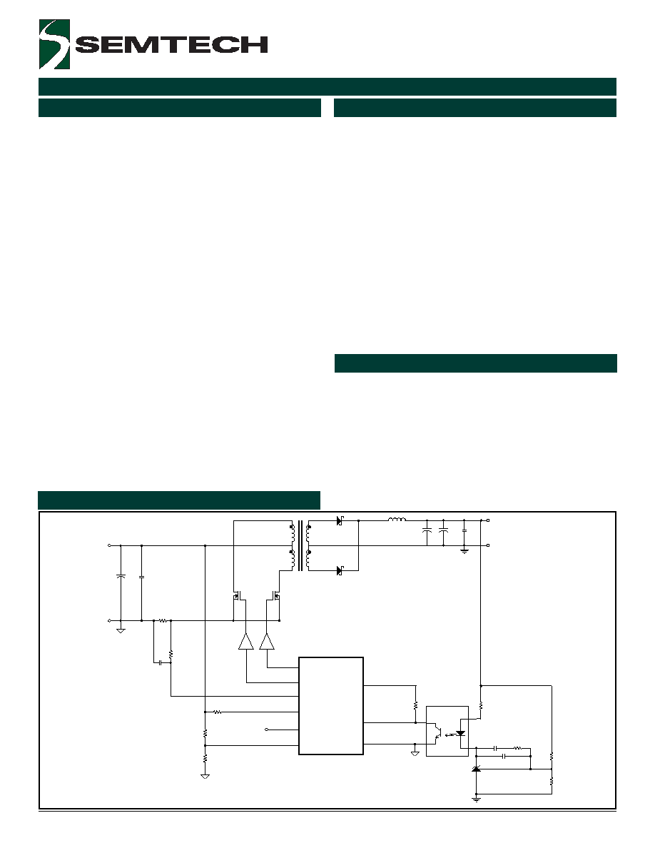
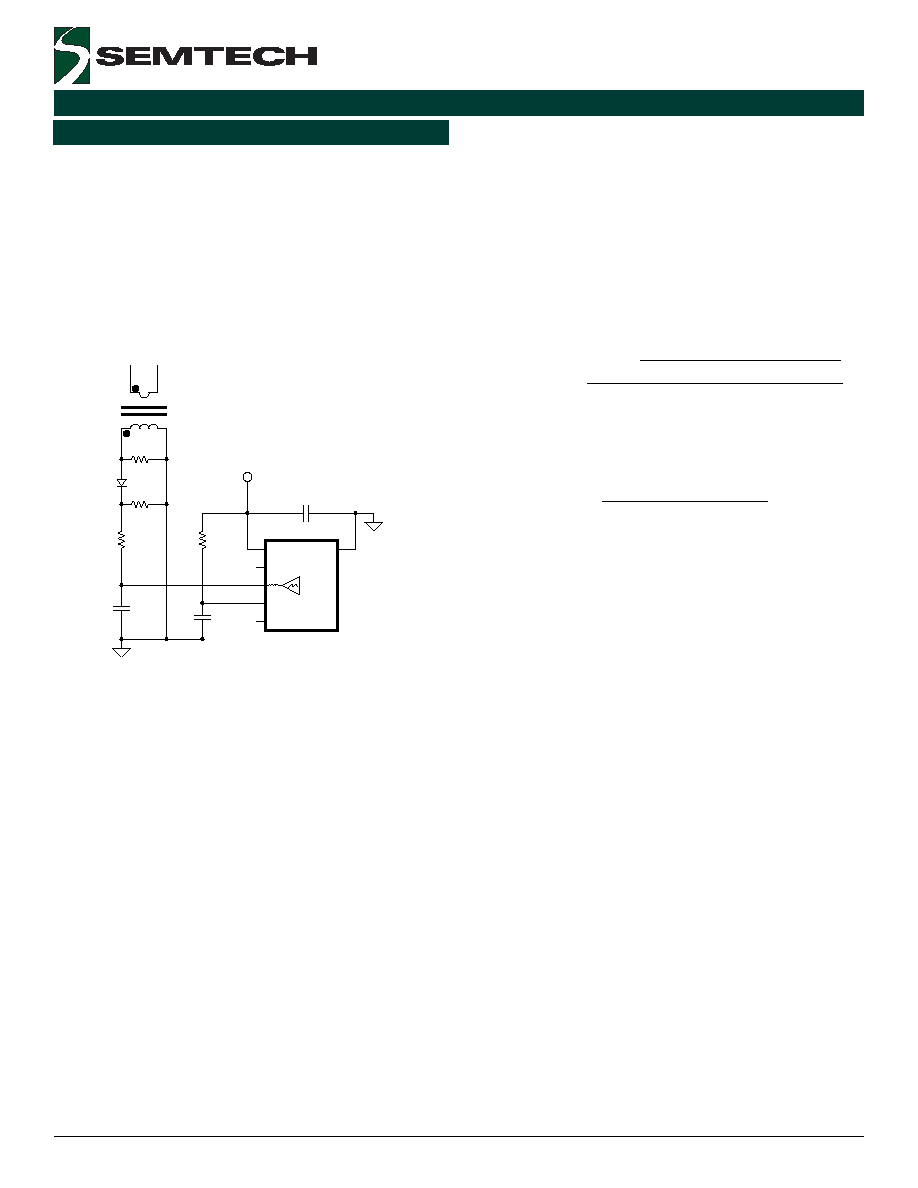
Typical Application Circuit
120µA starting current
Pulse by pulse current limit
Programmable operation up to 1MHz
Internal soft start
Programmable line undervoltage lockout
Over current shutdown
Dual output drive stages on push-pull configuration
Programmable internal slope compensation
Programmable mode of operation (peak current mode
or voltage mode)
External frequency synchronization
Bi-phase mode of operation
-40 to 105 ∞C operating temperature
MSOP-10 lead free package. This product is fully WEEE
and RoHS compliant
Telecom equipment and power supplies
Networking power supplies
Industrial power supplies
Push-pull converter
Half bridge converter
Full bridge converter
Isolated VRM's
Vo
Vin
RSENSE
Gnd_Out
SYNC
Gnd_In
FB
GND
REF
LUVLO
OUTA
OUTB
CS
VCC
SYNC
RC
SC4808
The SC4808B-2 is a dual-ended, high frequency, integrated
PWM controller, optimized for isolated applications that
require minimum space. It can be configured for current
or voltage mode operation with required control circuitry
where secondary side error amplifier is used.
Some of the key features are high frequency operation of
1 MHz that allows the use of smaller components thus
saving cost and valuable board space. An internal ramp
on the Current Sense pin allows Internal Slope
Compensation programmed by an external resistor. Other
features include programmable frequency up to 1MHz,
Pulse by Pulse current and Line Monitoring Input with
Hysteresis to reduce stress on the power components.
A unique oscillator is used to synchronize two SC4808B-
2's to work out of phase. This minimizes the input and
output ripple thus reducing noise on the output line and
reducing stress and size of input/output filter components.
The dual outputs can be configured in Push-Pull, Half Bridge
and Full Bridge format with programmable dead time
between two outputs depending on the size of the timing
components.
The SC4808B-2 also features a turn on threshold of 4.4V
and is available in MSOP-10 package.
2
2005 Semtech Corp.
www.semtech.com
SC4808B-2
POWER MANAGEMENT
Absolute Maximum Ratings
Electrical Characteristics
r
e
t
e
m
a
r
a
P
s
n
o
i
t
i
d
n
o
C
t
s
e
T
n
i
M
p
y
T
x
a
M
t
i
n
U
M
W
P
e
l
c
y
C
y
t
u
D
m
u
m
i
x
a
M
,
V
5
=
B
F
,
z
H
k
0
5
=
c
s
o
F
B
T
U
O
r
o
A
T
U
O
t
a
d
e
r
u
s
a
e
M
8
4
9
4
0
5
%
e
l
c
y
C
y
t
u
D
m
u
m
i
n
i
M
,
V
5
.
1
=
B
F
,
z
H
k
0
5
=
c
s
o
F
B
T
U
O
r
o
A
T
U
O
t
a
d
e
r
u
s
a
e
M
0
%
e
s
n
e
S
t
n
e
r
r
u
C
n
i
a
G
3
l
a
n
g
i
S
t
u
p
n
I
m
u
m
i
x
a
M
5
7
4
5
2
5
5
7
5
V
m
y
a
l
e
D
t
u
p
t
u
O
o
t
S
C
0
0
1
s
n
d
l
o
h
s
e
r
h
T
t
n
e
r
r
u
C
r
e
v
O
0
5
8
.
0
5
9
.
1
V
r
o
t
s
i
s
e
R
n
o
it
a
s
n
e
p
m
o
C
e
p
o
l
S
l
a
n
r
e
t
n
I
5
2
k
t
e
s
ff
O
S
C
o
t
B
F
0
3
.
1
0
5
.
1
0
7
.
1
V
t
u
p
t
u
O
l
e
v
e
L
w
o
L
T
U
O
0
0
5
.
0
7
.
V
l
e
v
e
L
h
g
i
H
T
U
O
0
.
1
1
5
2
.
1
1
0
0
.
2
1
V
e
m
i
T
e
s
i
R
5
2
s
n
e
m
i
T
ll
a
F
5
2
s
n
r
e
t
e
m
a
r
a
P
l
o
b
m
y
S
m
u
m
i
x
a
M
s
t
i
n
U
e
g
a
tl
o
V
y
l
p
p
u
S
V
C
C
8
1
o
t
5
.
0
-
V
t
n
e
r
r
u
C
y
l
p
p
u
S
I
C
C
0
2
A
m
D
N
G
o
t
F
E
R
,
O
L
V
U
L
,
S
C
,
C
R
,
C
N
Y
S
7
o
t
5
.
0
-
V
D
N
G
o
t
B
F
V
B
F
V
(
o
t
5
.
0
-
F
E
R
)
5
.
0
+
V
t
n
e
r
r
u
C
F
E
R
I
F
E
R
0
1
A
m
D
N
G
o
t
B
T
U
O
/
A
T
U
O
V
B
/
A
T
U
O
8
1
o
t
5
.
0
-
V
)
k
a
e
p
(
t
n
e
r
r
u
C
e
c
r
u
o
S
B
T
U
O
/
A
T
U
O
I
e
c
r
u
o
s
0
5
2
-
A
m
)
k
a
e
p
(
t
n
e
r
r
u
C
k
n
i
S
B
T
U
O
/
A
T
U
O
I
k
n
i
s
0
5
2
A
m
T
t
a
n
o
it
a
p
i
s
s
i
D
r
e
w
o
P
A
C
∞
5
2
=
P
D
5
0
1
.
1
W
e
c
n
a
t
s
i
s
e
R
l
a
m
r
e
h
T
A
J
1
.
3
1
1
W
/
C
∞
e
r
u
t
a
r
e
p
m
e
T
n
o
it
c
n
u
J
T
J
0
5
1
o
t
0
4
-
C
∞
e
g
n
a
R
e
r
u
t
a
r
e
p
m
e
T
e
g
a
r
o
t
S
T
G
T
S
0
5
1
o
t
5
6
-
C
∞
.
c
e
S
0
1
)
g
n
ir
e
d
l
o
S
(
e
r
u
t
a
r
e
p
m
e
T
d
a
e
L
T
D
A
E
L
0
0
3
+
C
∞
)l
e
d
o
M
y
d
o
B
n
a
m
u
H
(
g
n
it
a
R
D
S
E
V
D
S
E
2
V
k
Unless specified: VCC = 12V; CL = 100pF; T
A
= -40∞C to 105∞C
Exceeding the specifications below may result in permanent damage to the device, or device malfunction. Operation outside of the parameters specified in
the Electrical Characteristics section is not implied.
3
2005 Semtech Corp.
www.semtech.com
SC4808B-2
POWER MANAGEMENT
Electrical Characteristics (Cont.)
r
e
t
e
m
a
r
a
P
s
n
o
i
t
i
d
n
o
C
t
s
e
T
n
i
M
p
y
T
x
a
M
t
i
n
U
t
u
o
k
c
o
L
e
g
a
t
l
o
V
r
e
d
n
U
C
C
V
d
l
o
h
s
e
r
h
T
t
r
a
t
S
0
.
4
0
4
.
4
5
.
4
V
s
i
s
e
r
e
t
s
y
H
0
0
1
0
4
1
0
8
1
V
m
t
u
o
k
c
o
L
e
g
a
t
l
o
V
r
e
d
n
U
e
n
i
L
d
l
o
h
s
e
r
h
T
t
r
a
t
S
k
4
1
=
3
2
R
k
0
1
=
3
3
R
,
)
1
1
e
g
a
p
e
e
s
(
%
3
-
F
E
R
V
%
3
+
V
s
i
s
e
r
e
t
s
y
H
k
4
1
=
3
2
R
k
0
1
=
3
3
R
,
)
1
1
e
g
a
p
e
e
s
(
f
o
%
6
.
5
F
E
R
V
V
m
t
r
a
t
S
t
f
o
S
p
m
a
R
t
r
a
t
S
tf
o
S
l
a
n
r
e
t
n
I
0
0
2
V
/
s
µ
n
o
it
a
r
u
D
t
r
a
t
S
tf
o
S
k
1
=
s
c
R
n
o
it
a
c
il
p
p
a
e
h
t
n
i
a
l
u
m
r
o
f
e
e
S
(
)
8
1
e
g
a
p
n
o
n
o
it
c
e
s
n
o
it
a
m
r
o
f
n
i
2
1
s
µ
y
a
l
e
D
t
r
a
t
S
tf
o
S
0
4
1
s
µ
r
o
t
a
ll
i
c
s
O
y
c
n
e
u
q
e
r
F
r
o
t
a
ll
i
c
s
O
R
c
s
o
k
1
1
=
C
,
c
s
o
F
p
0
0
2
=
0
5
4
0
0
5
0
5
5
z
H
K
p
m
a
R
r
o
t
a
ll
i
c
s
O
2
/
F
E
R
V
5
2
.
0
+
V
e
c
n
a
ti
c
a
p
a
c
D
N
G
o
t
n
i
p
C
R
2
2
F
p
e
g
n
a
R
y
c
n
e
u
q
e
r
F
r
o
t
a
ll
i
c
s
O
0
5
0
0
0
1
z
H
K
K
C
O
L
C
/
c
n
y
S
d
l
o
h
s
e
r
h
T
C
N
Y
S
k
c
o
l
C
0
.
1
V
e
g
n
a
R
y
c
n
e
u
q
e
r
F
c
n
y
S
F
c
s
o
3
.
1
*
z
H
K
p
a
g
d
n
a
B
e
g
a
tl
o
V
e
c
n
e
r
e
f
e
R
0
7
9
.
2
5
2
1
.
3
0
8
2
.
3
V
e
c
n
e
r
e
f
e
R
t
n
e
r
r
u
C
5
A
m
ll
a
r
e
v
O
t
n
e
r
r
u
C
p
u
t
r
a
t
S
d
l
o
h
s
e
r
h
t
t
r
a
t
s
<
C
C
V
0
5
1
A
µ
t
n
e
r
r
u
C
y
l
p
p
u
S
g
n
it
a
r
e
p
O
V
0
=
S
C
,
V
0
=
B
F
7
A
m
e
g
a
tl
o
V
t
n
u
h
S
r
e
n
e
Z
C
C
V
A
m
0
1
=
D
D
I
6
1
V
Unless specified: VCC = 12V; CL = 100pF; T
A
= -40∞C to 105∞C
4
2005 Semtech Corp.
www.semtech.com
SC4808B-2
POWER MANAGEMENT
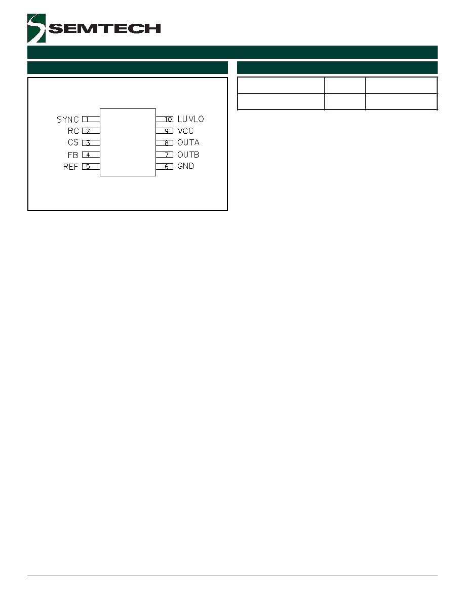
Pin Configuration
Ordering Information
r
e
b
m
u
N
t
r
a
P
e
g
a
k
c
a
P
T
(
e
g
n
a
R
.
p
m
e
T
A
)
T
R
T
S
M
2
-
B
8
0
8
4
C
S
)
2
(
)
1
(
0
1
-
P
O
S
M
C
∞
5
0
1
o
t
C
∞
0
4
-
(MSOP-10)
Top View
Notes:
(1) Only available in tape and reel packaging. A reel
contains 2500 devices.
(2) Lead free product. This product is fully WEEE and
RoHS compliant.

5
2005 Semtech Corp.
www.semtech.com
SC4808B-2
POWER MANAGEMENT
FB: The inverting input to the PWM comparator. Stray in-
ductances and parasitic capacitance should be minimized
by utilizing ground planes and correct layout guide lines
(see page 19).
REF: Bandgap reference output It should be by passed with
a 2.2uF low ESR capacitance, right at the IC pin.
CS: Current sense input and internal slope compensation
are both provided via the CS pin. The current sense input
from a sense resistor is used for the peak current and
overcurrent comparators. An internal 1 to 3 feed back volt-
age divider provides a 3X amplification of the CS signal.
This is used for comparison to the external error amplifier
signal. If an external resistor is connected from CS to the
current sense resistor, the internal current source will pro-
vide a programmable slope compensation. The value of
the resistor will determine the level of compensation. At
higher compensation levels, voltage mode of operation can
be achieved.
RC: The oscillator programming pin. The oscillator should
be referenced to a stable reference voltage for an accu-
rate and stable frequency. Only two components are re-
quired to program the oscillator, a resistor (tied to Vref and
RC), and a capacitor (tied to the RC and GND). The follow-
ing formula can be used for a close approximation of the
oscillator frequency.
8
.
0
1
_
◊
TOT
OSC
A
OSC
C
R
F
9
.
0
1
_
◊
TOT
OSC
B
OSC
C
R
F
where:
Circuit
SC
OSC
TOT
C
C
C
C
+
+
=
4808
pF
C
SC
22
4808
Where the frequency is in Hertz, resistance in ohms, and
capacitance in farads. The recommended range of timing
resistors is between 10 kohm and 200kohm and range of
timing capacitors is between 100pF and 1000pF. Timing
resistors less than 10 kohm should be avoided.
Refer to layout guide lines on (page 19) to achieve best
results.
LUVLO: Line undervoltage lockout pin. An external resis-
tive divider will program the undervoltage lockout level. The
external divider should be referenced to the quiet analog
ground (see page 19). During the LUVLO, the driver out-
puts are disabled and the softstart is reset. This pin can
also function as an Enable/Disable.
SYNC: SYNC is a positive edge triggered input with a thresh-
old set to 1.0V. In a single controller operation, SYNC could
be grounded or connected to an external synchronization
clock within the SYNC frequency range (see page 3). In
the Bi-Phase operation mode SYNC pins could be con-
nected to the Cosc (Timing Capacitors) of the other con-
troller. This will force an out of phase operation (see page
12).
GND: Device power and analog ground. Careful attention
should be paid to the layout of the ground planes (see page
19).
OUTA and OUTB: Out of phase gate drive stages. The
driver's peak source and sink current drive capability of
100mA, enables the use of an external MOSFET driver or
a NPN/PNP transistor buffer.
The oscillator RC network programs the oscillator frequency,
which is twice the OUTA/OUTB frequency. To insure that
the outputs do not overlap, a dead time can be generated
between the two outputs by sizing the oscillator timing
capacitor (see page 11).
VCC: The supply input for the device. Once VCC has ex-
ceeded the UVLO limit, the internal reference, oscillator,
drivers and logic are powered up. A low ESR capacitance,
should be used for decoupling right at the IC pin to mini-
mize noise problems.
Pin Descriptions
6
2005 Semtech Corp.
www.semtech.com
SC4808B-2
POWER MANAGEMENT
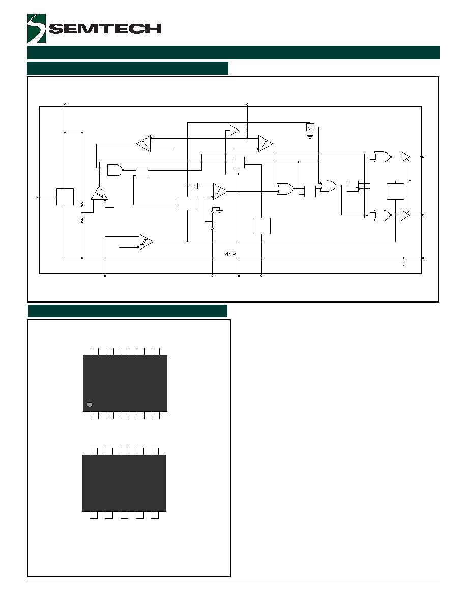
Block Diagram
FB
Peak Current
R
S
Q
SYNC
REF
OSC
VCC
RC
R
S
Q
SOFT
START
OUTB
CS
Enable
UVLO
OUTA
LUVLO
GND
SYNC
Bandgap
Disable
LUVLO
T
Q
Q
OVER CURRENT
LUVLO
Slope Comp.
R
2R
500mv
yyww = Datecode (Example: 9912)
xxxx = Semtech Lot # (Example: E901
xxxx
01-1)
Top Mark
yyww
xxxx
AB2B
Bottom Mark
xxxx
Marking Information
7
2005 Semtech Corp.
www.semtech.com
SC4808B-2
POWER MANAGEMENT
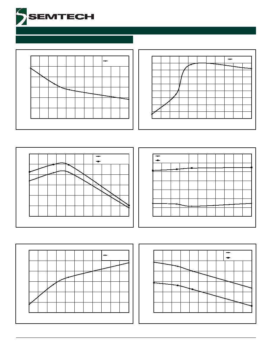
4.200
4.250
4.300
4.350
4.400
4.450
4.500
-40
-25
-10
5
20
35
50
65
80
95
110
125
Ta (∞C)
Vc
c
UV
L
O
(
V
)
Vcc UVLO (Rising)
Vcc UVLO (Falling)
3.60
3.65
3.70
3.75
3.80
3.85
3.90
-40
-25
-10
5
20
35
50
65
80
95
110
125
Ta (∞C)
Iq
(m
A)
Operating Iq, Vcc = 5V
Operating Iq, Vcc = 5.25V
SC4808B-2 Typical Characteristics
(SC4808B-2A)
Iq (start up) vs. Temperature
Iq (operating) vs. Temperature
Reference vs. Temperature
FB to CS Offset vs. Temperature
Current sense vs. Temperature
Vcc UVLO vs. Temperature
400
500
600
700
800
900
1000
1100
-40
-25
-10
5
20
35
50
65
80
95
110
125
Ta (∞C)
Curr
e
n
t
Se
ns
e
(
m
V)
Max Current Sense Signal
Over Current Signal
1.60
1.61
1.62
1.63
1.64
1.65
1.66
1.67
1.68
1.69
-40
-25
-10
5
20
35
50
65
80
95
110
125
Ta (∞C)
FB
t
o
C
S
of
fs
et
(
V
)
FB to CS Offset
3.16
3.17
3.18
3.19
3.2
3.21
3.22
-40
-25
-10
5
20
35
50
65
80
95
110
125
Ta (∞C)
R
e
fe
re
n
ce (V
)
Reference, Vcc = 5V
70.0
75.0
80.0
85.0
90.0
95.0
100.0
-40
-25
-10
5
20
35
50
65
80
95
110
125
Ta (∞C)
Iq
(
u
A)
Start up Iq, Vcc = 4V
8
2005 Semtech Corp.
www.semtech.com
SC4808B-2
POWER MANAGEMENT
100
105
110
115
120
125
130
135
140
-40
-25
-10
5
20
35
50
65
80
95
110
125
Ta (∞C)
L
U
V
L
O
H
y
st
er
es
is
(m
V
)
LUVLO (Hysteresis)
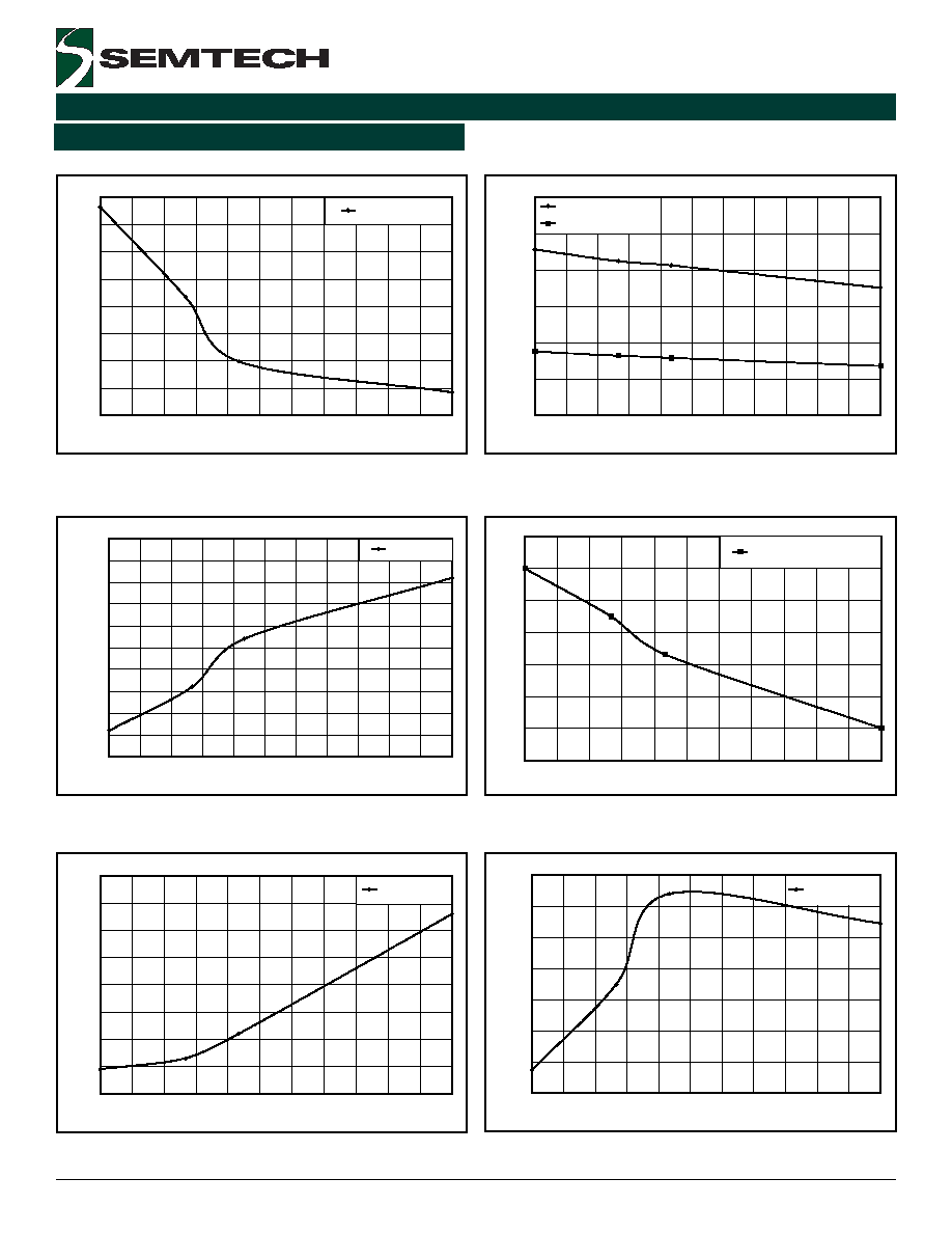
Vcc UVLO Hysteresis vs. Temperature
Line UVLO vs. Temperature
Line UVLO Hysteresis vs. Temperature
Oscillator Frequency vs. Temperature
Synchronization Frequency vs. Temperature
Maximum Duty Cycle vs. Temperature
SC4808B-2 Typical Characteristics (Cont.)
49.4
49.4
49.4
49.4
49.4
49.5
49.5
49.5
-40
-25
-10
5
20
35
50
65
80
95
110
125
Ta (∞C)
M
a
x
i
m
u
m
D
u
t
y
C
ycl
e (%
)
Maximum Duty Cycle
650
652
654
656
658
660
662
664
-40
-25
-10
5
20
35
50
65
80
95
110
125
Ta (∞C)
Sync
hroni
z
a
t
i
on Fr
eque
ncy (
k
Hz
)
Sync. Frequency @ Fosc = 500kHz
200
400
600
800
1000
1200
1400
-40
-25
-10
5
20
35
50
65
80
95
110
125
Ta (∞C)
O
sci
ll
at
or
Fr
eq
u
e
n
cy (k
H
z
)
Oscillator Frequency 1MHz
Oscillator Frequency 500kHz
3.120
3.125
3.130
3.135
3.140
3.145
3.150
3.155
3.160
3.165
3.170
-40
-25
-10
5
20
35
50
65
80
95
110
125
Ta (∞C)
LU
VLO
(V)
LUVLO (Rising)
84
86
88
90
92
94
96
98
100
-40
-25
-10
5
20
35
50
65
80
95
110
125
Ta (∞C)
V
c
c U
V
L
O
H
y
st
er
es
i
s
(m
V
)
Vcc UVLO (Hysteresis)
9
2005 Semtech Corp.
www.semtech.com
SC4808B-2
POWER MANAGEMENT
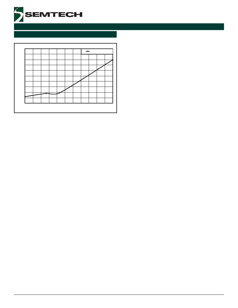
SC4808B-2 Typical Characteristics (Cont.)
Soft Start Delay time vs. Temperature
80
90
100
110
120
130
140
150
160
170
180
-40
-25
-10
5
20
35
50
65
80
95
110
125
Ta (∞C)
Sof
t
St
a
r
t
De
l
a
y
Ti
me
(
u
s
)
Soft Start Delay Time

10
2005 Semtech Corp.
www.semtech.com
SC4808B-2
POWER MANAGEMENT
age divider provides a 3X amplification of the CS signal.
This is used for comparison to the external error amplifier
signal. If an external resistor is connected from CS to the
current sense resistor, the internal current source will pro-
vide a programmable slope compensation. The value of
the resistor will determine the level of compensation. At
higher compensation levels, voltage mode of operation can
be achieved. The error amplifier signal at the FB pin will be
used in conjunction with the CS signal to achieve regula-
tion.
Two levels of undervoltage lockout are also available. The
LUVLO (line under voltage lockout) pin via an external re-
sistive divider will program the undervoltage lockout level.
During the LUVLO, the driver outputs are disabled and the
softstart is reset.
Once VCC has exceeded the UVLO (VCC under voltage lock-
out) limit, the internal reference, oscillator, drivers and logic
are powered up.
SYNC is a positive edge triggered input with a threshold
set to 1.0V.
By connecting an external control signal to the SYNC pin,
the internal oscillator frequency will be synchronized to the
positive edge of the external control signal. In a single con-
troller operation, SYNC should be grounded or connected
to an external synchronization clock within the SYNC fre-
quency range (see page 3).
In the Bi-phase operation mode a very unique oscillator
is utilized to allow two SC4808B-2 to be synchronized
together and work out of phase. This feature is setup by
simple connection of the SYNC input to the RC pin of the
other part. The fastest oscillator automatically becomes
the master, forcing the two PWMs to operate out of
phase. This feature minimizes the input and output
ripples, and reduces stress on the capacitors.
THEORY OF OPERATION
The SC4808B-2 is a versatile double ended, high speed,
low power, pulse width modulator that is optimized for ap-
plications requiring minimum space.
The device contains all of the control and drive circuity re-
quired for isolated or non isolated power supplies where
an external error amplifier is used. A fixed oscillator fre-
quency (up to 1MHz) can be programmed by an external
RC network.
The SC4808B-2 is a peak current or voltage mode
controller, depending on the amount of slope
compensation, programmable with only one external
resistor. The cycle by cycle peak current limit prevents core
saturation when a transformer is used for isolation while
the overcurrent circuitry initiates the softstart cycle.
The SC4808B-2 dual output drive stages are arranged in a
push-pull configuration. Both outputs switch at half the
oscillator frequency using a toggle flip flop. The dead time
between the two outputs is programmable depending on
the values of the timing capacitor and resistors, thus limiting
each output stage duty cycle to less than 50%.
The SC4808B-2 also provides flexibility with programmable
LUVLO thresholds, with built-in hysteresis.
SUPPLY
A single supply, VCC is used to provide the bias for the
internal reference, oscillator, drivers, and logic circuitry of
SC4808B-2. To ensure proper operation during start up,
VCC slew rate of less than 10V/mS is recommended.
PWM CONTROLLER
SC4808B-2 is a double ended PWM controller that can be
used in voltage or current mode applications. The
SC4808B-2 provides a 4.4V VCC UVLO, and a 3.125V ref-
erence. The oscillator frequency is programmed by a resis-
tor and a capacitor network connected to an external refer-
ence provided by the SC4808B-2. The two outputs, OUTA
and OUTB, are 180 degrees out of phase and run at half of
the oscillator frequency.
An external error amplifier will provide the error signal to
the FB pin of the SC4808B-2.
The current sense input and internal slope compensation
are both provided via the CS pin. The current sense input
from a sense resistor is used for the peak current and
overcurrent comparators. An internal 1 to 3 feedback volt-
Application Information
11
2005 Semtech Corp.
www.semtech.com
SC4808B-2
POWER MANAGEMENT
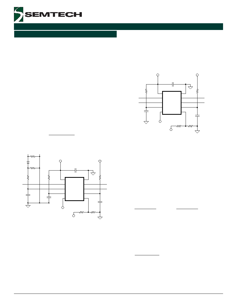
VCC UNDER VOLTAGE LOCK OUT
Depending on the application and the voltages available,
the SC4808B-2 (UVLO = 4.4V) can be used to provide the
VCC undervoltage lock out function to ensure the convert-
ers controlled start up.
Before the VCC UVLO has been reached, the internal refer-
ence, oscillator, OUTA/OUTB drivers, and logic are disabled.
LINE UNDER VOLTAGE LOCK OUT
The SC4808B-2 also provides a line undervoltage (LUVLO
= Vref) function. The LUVLO pin is programmed via an ex-
ternal resistor divider connected as shown below. The ac-
tual start-up voltage can be calculated by using the equa-
tion below:
(
)
33
R
33
R
23
R
V
V
REF
Startup
+
◊
=
R27
15k
R24 10k
200p
C31
VCC
R26
2.2k
R28
10
2.2u,16V
C26
82p
C29
15
REF
0.1u,25V
C33
R25 18
R33
10k
SYNC
U4
SC4808
4
5
3
2
10
1
6
7
8
9
FB
REF
CS
RC
LUVLO
SYNC
GND
OUTB
OUTA
VCC
R23
56.2k
Vin
REFERENCE
A 3.125V(SC4808B-2) reference voltage is available that
can be used to source a typical current of 5mA to the ex-
ternal circuitry. The Vref can be used to provide the oscilla-
tor RC network with a regulated bias.
Application Information (Cont.)
OSCILLATOR
The oscillator frequency is set by connecting a RC network
as shown below.
0
R27
15k
0
200p
C31
VCC
R28
10
2.2u,16V
C26
REF
0.1u,25V
C33
R33
10k
SYNC
U4
SC4808
4
5
3
2
10
1
6
7
8
9
FB
REF
CS
RC
LUVLO
SYNC
GND
OUTB
OUTA
VCC
R23
56.2k
Vin
The oscillator has a ramp voltage of about Vref/2. The os-
cillator frequency is twice the frequency of the OUTA and
OUTB gate drive controls.
The oscillator capacitor C31 is charged by a current sourced
from the Vref through R27. Once the RC pin reaches about
Vref/2, the capacitor is discharged internally by the
SC4808B-2. It should be noted that larger capacitor val-
ues will result in a longer dead time during the down slope
of the ramp.
The following equation can be used as an approximation
of the oscillator frequency and the Dead time:
8
.
0
1
_
◊
TOT
OSC
A
OSC
C
R
F
9
.
0
1
_
◊
TOT
OSC
B
OSC
C
R
F
where:
Circuit
SC
OSC
TOT
C
C
C
C
+
+
=
4808
pF
C
SC
22
4808
3
10
3
5
.
0
-
◊
◊
REF
OSC
deadtime
V
C
T
The recommended range of timing resistors is between 10
kohm and 200kohm, range of timing capacitors is between
100pF and 1000pF. Timing resistors less than 10 kohm
should be avoided.
12
2005 Semtech Corp.
www.semtech.com
SC4808B-2
POWER MANAGEMENT
SYNC/Bi-Phase operation
In noise sensitive applications where synchronization of
the oscillator frequency to a reference frequency is required,
the SYNC pin can accept the external clock. By connecting
an external control signal to the SYNC pin, the internal os-
cillator frequency will be synchronized to the positive edge
of the external control signal. SYNC is a positive edge trig-
gered input with a threshold set to 1.0V (SC4808B-2).
In a single controller operation, SYNC should be grounded
or connected to an external synchronization clock within
the SYNC frequency range (see page 3).
U2
SC4808
4
5
3
2
10
1
6
7
8
9
FB
REF
CS
RC
LUVLO
SYNC
GND
OUTB
OUTA
VCC
Cosc1
U1
SC4808
4
5
3
2
10
1
6
7
8
9
FB
REF
CS
RC
LUVLO
SYNC
GND
OUTB
OUTA
VCC
REF
Rosc2
REF
Rosc1
Cosc2
In the Bi-phase operation mode a very unique oscillator is
utilized to allow two SC4808B-2's to be synchronized
together and work out of phase. This feature is set up by a
simple connection of the SYNC input to the RC pin of the
other part. The fastest oscillator automatically becomes
the master, forcing the two PWMs to operate out of phase.
This feature minimizes the input and output ripples, and
reduces stress on the capacitors.
Application Information (Cont.)
FEED BACK
The error signal from the output of an external error ampli-
fier such as SC431 or SC4431 is applied to the inverting
input of the PWM comparator at the FB pin either directly
or via an opto coupler for the isolated applications. For best
stability, keep the FB trace length as short as possible.
C39
22n
C38
0.1u
Vref
SC4431
1
2
4
5
R35
C36
C35
R34
R36
R38
C37
R32
Vout
Vout
C40
22pF
R37
2.2k
MOCD207
3
4
6
5
Vref
FB
The signal at the FB pin is then compared to the 3X ampli-
fied signal from the current sense/ slope compensation
CS pin. Matched out of phase signals are generated to
control the OUTA and OUTB gate drives of the two phases.
A single ramp signal is used to generate the control sig-
nals for both phases, hence achieving a tightly matched
per phase operation.
Voltages below 1.5V at the FB pin, will produce a 0% duty
cycle at the OUTA/OUTB gate drives. This offset is to pro-
vide enough head room for the opto coupler used in iso-
lated applications.
GATE DRIVERS
OUTA and OUTB are out of phase bipolar gate drive output
stages, that are supplied from VCC and provide a peak
source/sink current of about 100mA. Both stages are ca-
pable of driving the logic input of external MOSFET drivers
or a NPN/PNP transistor buffer. The output stages switch
at half the oscillator frequency. When the voltage on the
RC pin is rising, one of the two outputs is high, but during
fall time, both outputs are off. This "dead time" between
the two outputs, along with a slower output rise and fall
time, insures that the two outputs can not be on at the
same time. The dead time is programmable and depends
upon the timing capacitor.
OUTA (PWM1)
OUTB (PWM1)
OUTA (PWM2)
OUTB (PWM2)
13
2005 Semtech Corp.
www.semtech.com
SC4808B-2
POWER MANAGEMENT
It should be noted that if high speed/high current drivers
such as the SC1301 are used, careful layout guide lines
must be followed in order to minimize stray inductance,
which might cause negative voltages at the output of the
drivers. This negative voltage can be clamped to a reason-
able level by placing a small Schottky diode directly at the
output of the driver as shown below.
C34
0.1u
VCC
VCC
U3
SC1301A
1
4
3
2
5
C23
0.1u
EN
U6
SC1301A
1
4
3
2
EN
VCC
R28
10
2.2u,16V
C26
F
D_A
0.1u,25V
C33
R33
10k
SYNC
U4
SC4808
4
5
3
2
10
1
6
7
8
9
FB
REF
CS
RC
LUVLO
SYNC
GND
OUTB
OUTA
VCC
D_B
Gate_A
5
Gate_B
R23
56.2k
Vin
OVER CURRENT
Two levels of over current protection are provided by the
SC4808B-2. The current information is sensed at the CS
pin and compared to a peak current limit level of 525mV.
If the 525mV limit is exceeded, the OUTA and OUTB pulse
widths and duty cycle is reduced until the CS pin reaches a
second threshold of 950mV. At that point, the OUTA and
OUTB are disabled, and after a delay of 140µs, the inter-
nal softstart sequence is started. After the softstart dura-
tion (see page 21 for calculation of softstart time), normal
operation is achieved, unless the over current condition is
still present.
Application Information (Cont.)
14
2005 Semtech Corp.
www.semtech.com
SC4808B-2
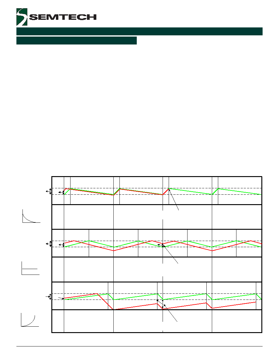
POWER MANAGEMENT
D<50%
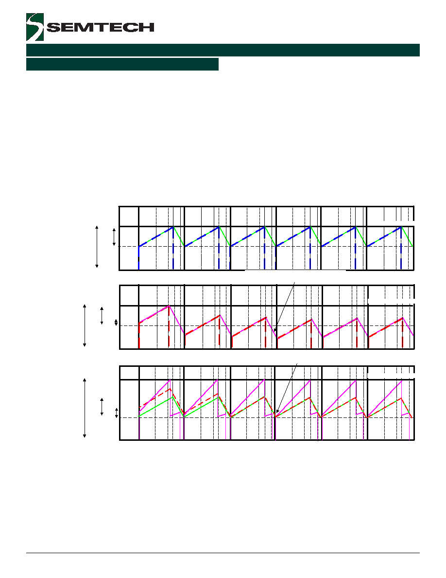
Instability in current mode operation
due to Duty cycle >50%
I
L
: Inductor current
i
L
: Small Inductor current perturbation
I
L
i
L
Note: After afew c ycles the perturbation
disappears and stable operation returns.
D=50%
I
L
i
L
i
L
I
L
Note: After afew c ycles the perturbation
is still pres ent, although this w ill caus e
jitter, but there is no instability.
D>50%
i
L
Note: After afew c ycles the perturbation
becomes larger, and causes instability.
i
L
Er
r
o
r
Time
Er
r
o
r
Time
Er
r
o
r
Time
SLOPE COMPENSATION (Current or Voltage mode of operation)
In applications where a current mode control is used for regulation, the peak inductor current information is used to
produce the average output current. If a small perturbation due to changes in supply voltage or noise pick up is gener-
ated, instability may occur if the duty cycle is >50%.
This phenomenon is graphically shown below. The inductor current and disturbed inductor current are shown for three
different duty cycles conditions.
The top wave form shows the applications where the duty cycle D is less than 50%. As shown, even if an error is
introduced, after only a few cycles the error converges to zero.
The second wave form shows the case where D = 50%. Under this condition, even though the error does not completely
disappear, it stays constant and is not getting larger. This will be seen as jitter at the inductor voltage.
The bottom wave form shows D>50%. As shown, a very small error results in a much larger error only after a few cycles.
This will cause instability in the converter and the average output inductor current. The output load will not be able to be
kept in regulation.
Application Information (Cont.)
15
2005 Semtech Corp.
www.semtech.com
SC4808B-2
POWER MANAGEMENT
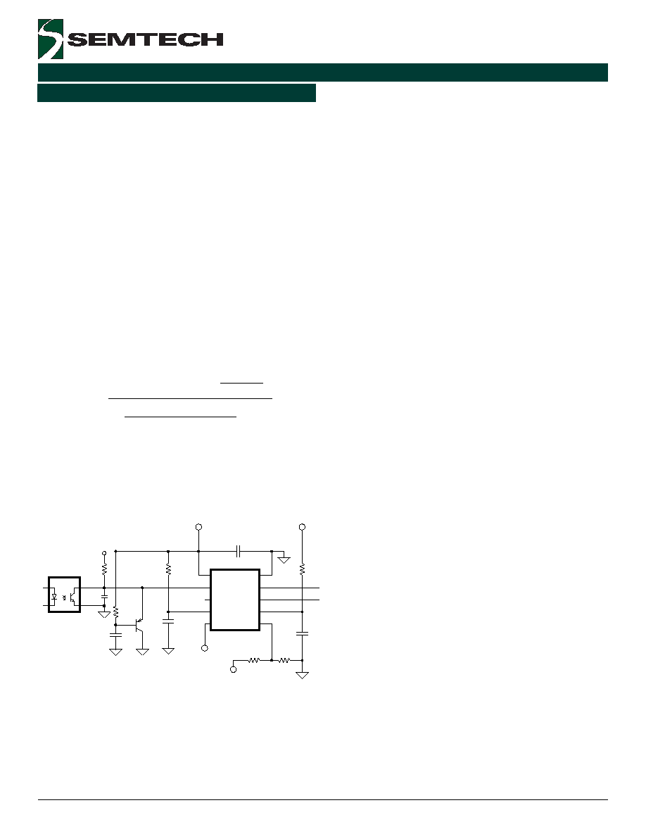
The instability can be corrected by modification of the peak
current information slope. One of the methods to alter the
peak current information is to add a positive going ramp to
the output of the current sensing circuitry.
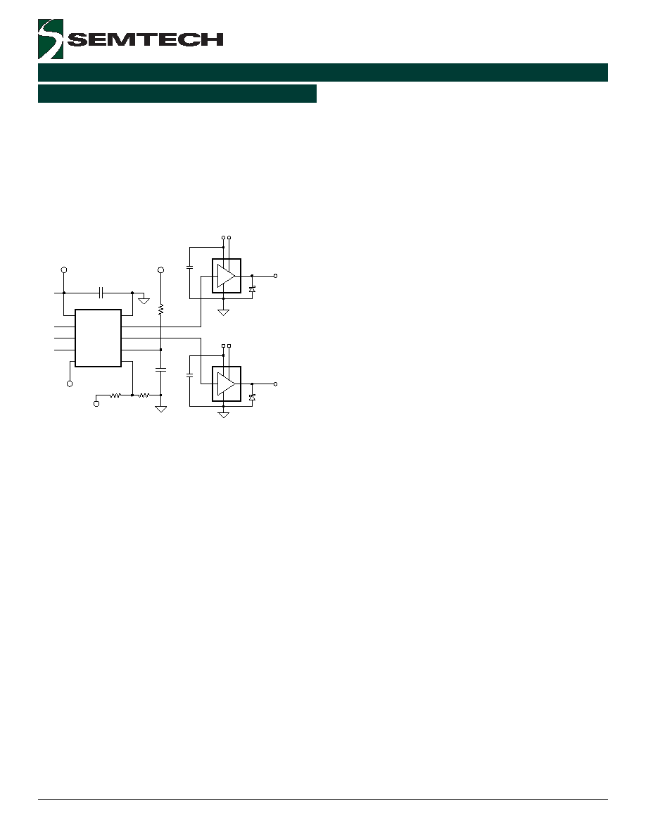
The SC4808B-2 achieves this by using an internal slope
compensation circuit. The oscillator ramp is internally buff-
ered and an internal 25kOhms resistor in conjunction with
an external resistor at the CS pin will program the level of
slope compensation.
Rosc
15k
R
10k
200p
Cosc
RSlope Comp
2.2u,16V
C
82p
Cfilter
D
REF
Rsense
SC4808
4
5
3
2
1
6
7
FB
REF
CS
RC
SYNC
GND
N = 100
25k
Current Transformer
RSlope Comp value will determine the Mode of operation (Voltage or Current)
The Peak current information is sensed and the result is
realistically summed to the buffered oscillator ramp, as
shown above. The value of the external resistor R
slope comp
will determine the percentage of the slope compensation.
As the value for R
slope comp
is reduced, the current informa-
tion becomes more dominant and the mode of operation
becomes more current mode. At the same time the slope
of the current information is modified to provide the slope
compensation.
Application Information (Cont.)
If the R
slope comp
is increased, the internal ramp becomes the
dominant signal and more voltage mode of operation is
achieved. As it can be calculated from the second formula
below, a 100% voltage mode operation can be achieved by
choosing R
slope comp
to be greater
than 6.25K ohms. Also if a
100% current mode of operation is required, R
slope comp
is
reduced to zero and the contribution from the internal ramp
is completely eliminated.
(
)
(
)
CS
ernal
int
sense
Comp
_
slope
sense
Comp
_
slope
Ramp
V
R
R
R
R
R
V
Comp
_
Slope
%
+
+
+
◊
=
or
(
)
(
)
◊
-
◊
∑
Comp
_
slope
%
2
.
0
1
Comp
_
slope
%
2
.
0
R
R
ernal
int
external
Next page illustrates how the buffered oscillator ramp is
used to modify the sensed inductor current.
It should be noted that in order for the slope compensa-
tion to be effective, the current sensed signal slope should
be at least 50% less steeper than the oscillator positive
ramp slope. The slope will include the magnetizing current
of the transformer and the inductor output current in iso-
lated applications. In non-isolated applications, the slope
will only include the inductor output current.
16
2005 Semtech Corp.
www.semtech.com
SC4808B-2
POWER MANAGEMENT
Slope Compensation generation from
Buffered Oscillator Ramp
I
L
: Inductor current
: Sm all Inductor current perturbation
I
L
D>50%
i
L
Note: Below wave forms are not to scale.
I
Sense
: Sensed Mosfet current
Buffered
Oscillator
Ramp
I
Sense
I
CS
: Summation of Isense and slope compensation, at the CS pin of the SC4808.
I
CS
Application Information (Cont.)
17
2005 Semtech Corp.
www.semtech.com
SC4808B-2
POWER MANAGEMENT
Application Information (Cont.)
Below the benefits from the slope compensation become apparent. The top wave form shows the stable operation
before the perturbation. The second wave form shows the perturbation and the instability caused from it if no slope
compensation is added to the current information. The last wave form shows the slope compensation and the effect of
it. The increase in the slope of the current information results in an early termination of the inductor current, hence a
reduction in the amount of error. As the cycle is repeated, the perturbation is reduced and finally eliminated.
Stable current mode operation with Slope
Compensation
I
L
: Inductor current
: Small Inductor current perturbation
I
L
D>50%
i
L
: Sensed Mosfet current
I
Sense
I
Sense
i
L
i
L
Stable operation
( no perturbation)
Instable operation
( with perturbation)
Stable operation
(Slope Compensation Added)
I
L
I
Sense
I
L
I
CS
Error Signal from Error amplifier
Error Signal from Error amplifier
I
CS
: Summation of Isense and slope compensation, at the CS pin of the SC4808.
Error Signal from Error amplifier
Note: After a few cycles the perturbation
disappears and stable operation returns.
Note: After a few cycles the perturbation
becomes larger, and causes instability.
18
2005 Semtech Corp.
www.semtech.com
SC4808B-2
POWER MANAGEMENT
SOFT START
During start up of the converter, the discharged output ca-
pacitor and the load current have large supply current re-
quirements. To avoid this a soft start scheme is usually
implemented where the duty cycle of the regulator is gradu-
ally increased from 0% until the soft start duration is
elapsed.
SC4808B-2 has an internal soft start circuit that limits the
duty cycle for a duration approximated by the formula be-
low. Also the soft start circuitry is activated if an over cur-
rent condition occurs. After an over current condition, OUTA
and OUTB are disabled and kept low for a duration of about
140µs. After the delay, the OUTA and OUTB are enabled
while the soft start limits the duty cycle. If the over current
condition persists, the soft start cycle repeats indefinitely.
Approximate internal soft start duration can be calculated
as below:
(
)
+
◊
1
R
R
2
VREF
Ramp
T
GND
_
to
_
CS
SlopeComp
_
Internal
SoftStart
SoftStart
If longer soft start durations are required, the simple exter-
nal circuit shown below can be implemented.
R27
15k
200p
C31
VCC
R28
10
2.2u,16V
C26
REF
0.1u,25V
C33
R33
10k
SYNC
U4
SC4808
4
5
3
2
10
1
6
7
8
9
FB
REF
CS
RC
LUVLO
SYNC
GND
OUTB
OUTA
VCC
R23
56.2k
Vin
56.2K
Csoft start
REF
MOCD207
6
5
C40
NA
R37
1k
Approximate soft start duration can be calculated as be-
low:
37
R
C
T
SoftStart
SoftStart
◊
Application Information (Cont.)
START UP SEQUENCE
Initially during the power up, the SC4808B-2 is in under
voltage lock out condition. As the Vcc supply exceeds the
UVLO limit of the SC4808B-2, the internal reference, oscil-
lator, and logic circuitry are powered up.
The OUTA and OUTB drivers are not enabled until the line
under voltage lock out limit is reached. At that point, once
the FB pin is above 1.5V, soft start circuitry starts the out-
put drivers, and gradually increases the duty cycle from
0%. The soft start duration is internally set (see formula in
Soft Start section).
As the output voltage starts to increase, the error signal
from the error amplifier starts to decrease. If isolation is
required, the error amplifier output can drive the LED of
the opto isolator. The output of the opto is connected in a
common emitter configuration with a pull-up resistor to a
reference voltage connected to the FB pin of the SC4808B-
2. The voltage level at the FB pin provides the duty cycle
necessary to achieve regulation.
If an over current condition occurs, the outputs are dis-
abled and after a soft start delay time of about 100µs, the
softstart sequence mentioned above is repeated.

19
2005 Semtech Corp.
www.semtech.com
SC4808B-2
POWER MANAGEMENT
7) If an Opto isolator is used for isolation, quiet primary
and secondary ground planes should be used. The same
precautions should be followed for the primary GND plane
as mentioned in item 5 mentioned above. For the second-
ary GND plane, the GND plane method mentioned in item
4 should be followed.
8) All the noise sensitive components such as LUVLO re-
sistive divider, reference by pass capacitor, Vcc bypass ca-
pacitor, current sensing circuitry, feedback circuitry, and
the oscillator resistor/capacitor network should be con-
nected as close as possible to the SC4808B-2. The GND
return should be connected to the quiet SC4808B-2 GND
plane.
9) The connection from the OUTA and OUTB of the
SC4808B-2 should be minimized to avoid any stray induc-
tance. If the layout can not be optimized due to constraints,
a small Schottky diode may be connected from the OUTA/
B pins to the ground directly at the IC. This will clamp ex-
cessive negative voltages at the IC. If drivers are used, the
Schottky diodes should be connected directly at the IC from
the output of the driver to the driver ground (See page 9).
10) If the SYNC function is not used, the SYNC pin should
be grounded at the SC4808B-2 GND to avoid noise pick
up.
Application Information (Cont.)
LAYOUT GUIDELINES
Careful attention to layout requirements are necessary for
successful implementation of the SC4808B-2 PWM con-
troller.
High current switching is present in the application and
their effect on ground plane voltage differentials must be
understood and minimized.
1). The high power parts of the circuit should be laid out
first. A ground plane should be used, the number and po-
sition of ground plane interruptions should be such as to
not unnecessarily compromise ground plane integrity. Iso-
lated or semi-isolated areas of the ground plane may be
deliberately introduced to constrain ground currents to
particular areas, such as the input capacitor and FET
ground.
2). In the loop formed by the Input Capacitor(s) (Cin), the
FET must be kept as small as possible. This loop contains
all the high current, fast transition switching. Connections
should be as wide and as short as possible to minimize
loop inductance. Minimizing this loop area will a) reduce
EMI, b) lower ground injection currents, resulting in electri-
cally "cleaner" grounds for the rest of the system and c)
minimize source ringing, resulting in more reliable gate
switching signals.
3). The connection between FETs and the Transformer
should be a wide trace or copper region. It should be as
short as practical. Since this connection has fast voltage
transitions, keeping this connection short will minimize EMI.
4) The Output Capacitor(s) (Cout) should be located as close
to the load as possible. Fast transient load currents are
supplied by Cout only, and connections between Cout and
the load must be short, wide copper areas to minimize in-
ductance and resistance.
5) The SC4808B-2 is best placed over a quiet ground plane
area. Avoid pulse currents in the Cin FET loop flowing in
this area. GND should be returned to the ground plane close
to the package and close to the ground side of (one of) the
VCC supply capacitor(s). Under no circumstances should
GND be returned to a ground inside the Cin, Q1, Q2 loop.
Avoid making a star connection between the quiet GND
planes that the SC4808B-2 will be connected to and the
noisy high current GND planes connected to the FETs.
6) The feed back connection between the error amplifier
and the FB pin should be kept as short as possible The
GND connections should be connected to the quiet GND
used for the SC4808B-2.

20
2005 Semtech Corp.
www.semtech.com
SC4808B-2
POWER MANAGEMENT
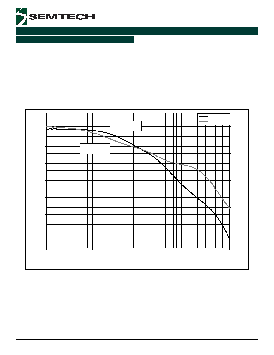
Gain & Phase Margin
Typical SC4808B-2 Push Pull Converter Gain/Phase plot at Vin = 36V, Vout = 3.3V, Iout = 10A, Fosc = 650kHz
-30
-20
-10
0
10
20
30
40
50
10
100
1000
10000
100000
Freq (Hz)
G
a
in
(d
B
)
-225
-180
-135
-90
-45
0
45
90
135
180
225
Phas
e (
d
e
g
)
Gain
Phase (deg)
Gain
Phase
21
2005 Semtech Corp.
www.semtech.com
SC4808B-2
POWER MANAGEMENT
Typical SC4808B-2 Push Pull Converter Gain/Phase plot at Vin = 48V, Vout = 3.3V, Iout = 10A, Fosc = 650kHz
Gain & Phase Margin (Cont.)
-30
-20
-10
0
10
20
30
40
50
10
100
1000
10000
100000
Freq (Hz)
G
a
in
(d
B
)
-225
-180
-135
-90
-45
0
45
90
135
180
225
Phase
(
d
eg
)
Gain
Phase (deg)
Gain
Phase

22
2005 Semtech Corp.
www.semtech.com
SC4808B-2
POWER MANAGEMENT
Gain & Phase Margin (Cont.)
Typical SC4808B-2 Push Pull Converter Gain/Phase plot at Vin = 72V, Vout = 3.3V, Iout = 10A, Fosc = 650kHz
-30
-20
-10
0
10
20
30
40
50
10
100
1000
10000
100000
Freq (Hz)
Ga
in (dB)
-225
-180
-135
-90
-45
0
45
90
135
180
225
Phase
(
d
eg
)
Gain
Phase (deg)
Gain
Phase
23
2005 Semtech Corp.
www.semtech.com
SC4808B-2
POWER MANAGEMENT
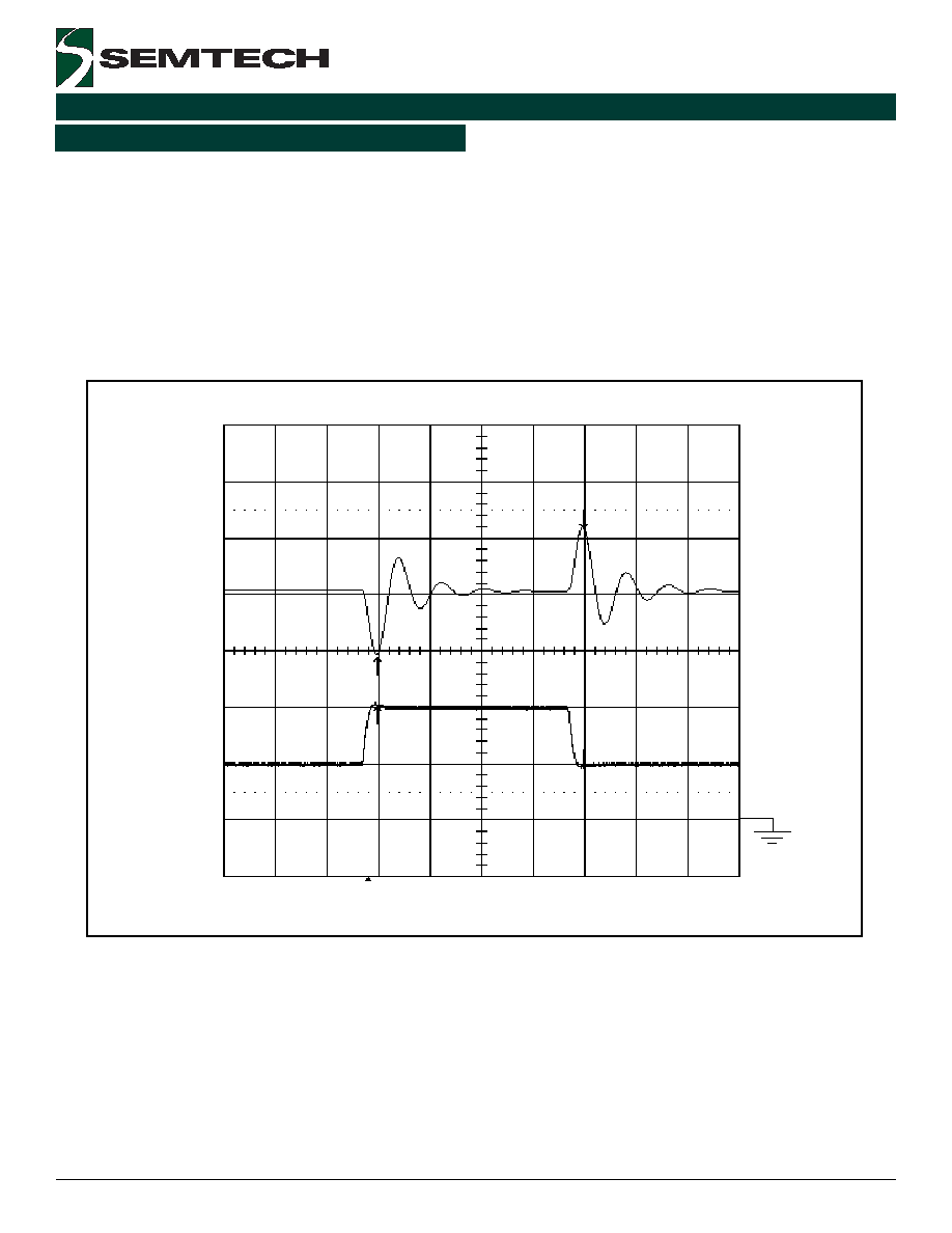
Typical Step Load
Typical SC4808B-2 Push Pull Converter Step Load plot at Vin = 48V, Vout = 3.3V, Step = 37% to 75% Iout, Fosc = 650kHz
Cout = 6X22uF (132uF) Ceramic
Iout
5A/Div
Vout
500mV/Div
100us/Div
24
2005 Semtech Corp.
www.semtech.com
SC4808B-2
POWER MANAGEMENT
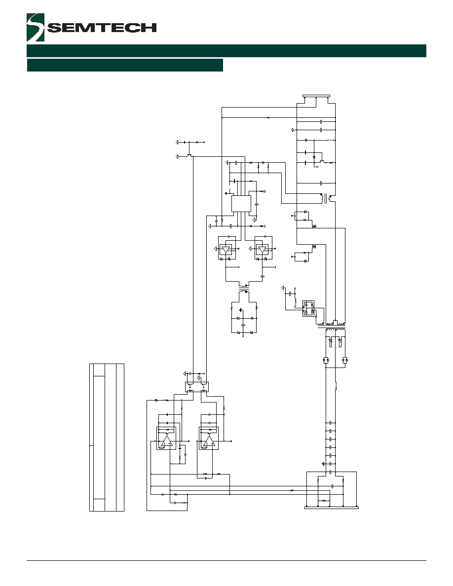
Evaluation Board Schematics
Sync Drive Supply
1u,16V
C20
.1u,16V
C14
M2
SUD19N20-90
3
2
1
R4
250
Q1 FZT853
E
B
C
C30
1nF
R31
16.2
Murata GRM32DR60J226KA01
D2
MBRB2535CTL
1
3
4
R29
100
CON2
3input_half_brick
1
2
4
V
in+
ON/OFF
Vin-
D3
1N5819HW
A
C
R19
0
C34
.1uF
For output power > 30W, adequate air flow should be provided to avoid over dissipation.
SC4808EVB__non_sync
1.1
SC4808 Push Pull 3.3V 50W non Synchronous
11
Monday, October 07, 2002
Title
Size
Document Number
Rev
Date:
Sheet
of
SEMTECH CORPORATION
D14
CMOSH-3
R27
15k
VCC = 15V
1u,100V
C11
D6
1N5819HW
D13
CMOSH-3
C24
0.1u
R3
20k
R12
56.2k
22u,6.3V
C6
0.1u,25V
C23
G_B
N = 100
T2
P8208T
8
7
1
3
G_A
M1
SUD19N20-90
3
2
1
R23
18.2k
1u,100V
C12
GRM55DR72E105KW01
R22
37.4k
R30
15k
D8
LS4448
D11
CMOSH-3
J2
0.1u
C10
0
J3
C26
0.1u
R26
2.2k
VCC
R21
10k
J1
T3
PE-68386
1
3
6
4
R25
11.5k
R24
1k
C3
2.2n
R32
56.2k
0.1u
C2
R8
0
VCC
2.2u,16V
C19
D15
CMOSH-3
R18
10
D12
CMOSH-3
Sync Drive Supply
R5
10
D1
MBRB2535CTL
1
3
4
C35
2.2uF 16V
Vref
U5
SC4431
1
2
4
5
D4
ZM4743A
22u,6.3V
C7
D16
1N5819HW
A
C
REF
REF
U3
SC1301A
1
4
3
2
5
R17
15k
R6
TBD
U1
SC4808
4
5
3
2
10
1
6
7
8
9
FB
REF
CS
RC
LUVLO
SYNC
GND
OUTB
OUTA
VCC
D7
CMOSH-3
D9
CMOSH-3
U2
SC1301A
1
4
3
2
5
22u,6.3V
C9
R7
0
C32
0.1u
R13
10k
82p
C22
U7
CBRHD-02
1
2
3
4
C1
2.2n
R1
0
R9
2.2
JP1
SYNC
G_B
C28
NA
Vref
U4
SC4431
1
2
4
5
L2
LQH43MN102K011
1
2
22u,6.3V
C4
R15
0
R20
2.2k
Sync Drive Supply
R11
TBD
R16
1k
R10
2.2
R28
25.5k
Q2 FMMT718
22u,6.3V
C8
VCC
D10
CMOSH-3
10u,16V
C15
GRM32DR61C106KA01
82p
C21
C25
10nF
22nF C18
R2
10
U6
MOCD207
1
2
8
7
3
4
6
5
10u,16V
C16
GRM32DR61C106KA01
C17
0.1u
G_A
VCC
VCC
C29
100pF
22u,6.3V
C5
D5
1N5819HW
CON1
5output_half_brick
5
6
7
8
9
Vout-
Sense-
Trim
Sense+
Vout+
C27
22n
C31
470pF
C33
22n
6T 1T
4T
T1
PA0500
2
5
3
4
10
9
8
1
6
R14
15
1u,100V
C13
GRM55DR72E105KW01
Note:
L1
0.9uH
1
2
0
REF
6T 1T
PG0006.102T
25
2005 Semtech Corp.
www.semtech.com
SC4808B-2
POWER MANAGEMENT
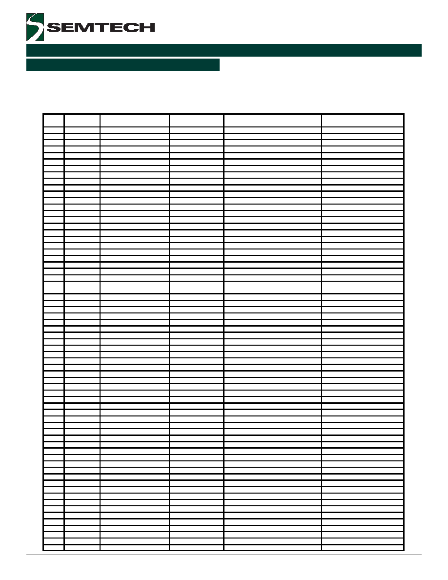
Evaluation Board Bill of Materials
SC4808 Push Pull 3.3V 50W non Synchronous
SC4808EVB__non_sync Revision: 1.1
Bill Of Materials October 7,2002 13:35:18
1
1
CON1
5output_half_brick
CON\5OUTPUT_HALF_BRICK
2
1
CON2
3input_half_brick
CON\3INPUT_HALF_BRICK
3
2
C3,C1
2.2n
SM/C_1206
4
6
C2,C10,C17,C24,C26,C32
0.1u
SM/C_0805
5
6
C4,C5,C6,C7,C8,C9
22u,6.3V
GRM32DR60J226KA01
SM/C_1210_GRM
6
3
C11,C12,C13
1u,100V
GRM55DR72E105KW01
SM/C_2220
7
1
C14
.1u,16V
SM/C_0805
8
2
C15,C16
10u,16V
GRM32DR61C106KA01
SM/C_1210_GRM
9
1
C18
22nF
SM/C_1206
10
1
C19
2.2u,16V
SM/C_1206
11
1
C20
1u,16V
GRM32RR71H105KA011
SM/C_1210_GRM
12
2
C22,C21
82p
SM/C_0805
13
1
C23
0.1u,25V
SM/C_1206
14
1
C25
10nF
SM/C_0805
15
2
C27,C33
22n
SM/C_0805
16
1
C28
NA
SM/C_0805
17
1
C29
100pF
SM/C_0805
18
1
C30
1nF
SM/C_0805
19
1
C31
470pF
SM/C_0805
20
1
C34
.1uF
SM/C_0805
21
1
C35
2.2uF 16V
SM/C_0805
22
2
D2,D1
MBRB2535CTL
DIODE_D2PAK
23
4
D3,D5,D6,D16
1N5819HW
SOD123
24
1
D4
ZM4743A
SMB/DO214
25
8
D7,D9,D10,D11,D12,D13,
CMOSH-3
CMOSH-3 (Central Semiconductor)
SOD523
D14,D15
26
1
D8
LS4448
SM/DO213AC
27
1
JP1
short
VIA\2P
28
1
J1
REF
ED5052
29
1
J2
Vcc
ED5052
30
1
J3
SYNC
ED5052
31
1
L1
0.9uH
PG0006
32
1
L2
LQH43MN102K011
LQH43MN102K01L
SDIP0302
33
2
M1,M2
SUD19N20-90
SUD19N20-90
DPAKFET
34
1
Q1
FZT853
SM/SOT223_BCEC
35
1
Q2
FMMT718
36
4
R1,R7,R15,R19
0
SM/R_0805
37
2
R5,R2
10
SM/R_1206
38
1
R3
20k
SM/R_1206
39
1
R4
250
SM/R_1210_MCR
40
2
R6,R11
TBD
SM/R_0805
41
1
R8
0
SM/R_1206
42
2
R9,R10
2.2
SM/R_0805
43
1
R12
56.2k
SM/R_1206
44
1
R13
10k
SM/R_0805
45
1
R14
15
SM/R_0805
46
2
R16,R24
1k
SM/R_0805
47
3
R17,R27,R30
15k
SM/R_0805
48
1
R18
10
SM/R_0805
49
2
R26,R20
2.2k
SM/R_0805
50
1
R21
10k
SM/R_1206
51
1
R22
37.4k
SM/R_0805
52
1
R23
18.2k
SM/R_0805
53
1
R25
11.5k
SM/R_0805
54
1
R28
25.5k
SM/R_0805
55
1
R29
100
SM/R_0805
56
1
R31
16.2
SM/R_1206
57
1
R32
56.2k
SM/R_0805
58
1
T1
PA0500
PA0500
59
1
T2
P8208T
P8208T
60
1
T3
PE-68386
PE-68386
61
1
U1
SC4808
MSOP10
62
2
U2,U3
SC1301A
SOT23_5PIN
63
2
U4,U5
SC4431
SOT23_5PIN
64
1
U6
MOCD207
SO-8
65
1
U7
CBRHD-02
CBRHD-02
Manufacturer #
Foot Print
Item
Quantity
Reference
Part
26
2005 Semtech Corp.
www.semtech.com
SC4808B-2
POWER MANAGEMENT
Evaluation Board Gerber Plots
Board Layout Assembly Top
Board Layout Assembly Bottom
Board Layout Top
Board Layout Bottom
27
2005 Semtech Corp.
www.semtech.com
SC4808B-2
POWER MANAGEMENT
Evaluation Board Gerber Plots
Board Layout INNER1
Board Layout INNER2
28
2005 Semtech Corp.
www.semtech.com
SC4808B-2
POWER MANAGEMENT
Outline Drawing - MSOP-10
Semtech Corporation
Power Management Products Division
200 Flynn Road, Camarillo, CA 93012
Phone: (805)498-2111 FAX (805)498-3804
Contact Information
bbb
C A-B D
DIMENSIONS "E1" AND "D" DO NOT INCLUDE MOLD FLASH, PROTRUSIONS
3.
OR GATE BURRS.
DATUMS AND TO BE DETERMINED AT DATUM PLANE
CONTROLLING DIMENSIONS ARE IN MILLIMETERS (ANGLES IN DEGREES).
-B-
NOTES:
1.
2.
-A-
-H-
SIDE VIEW
A
B
C
D
H
PLANE
0∞
.010
.004
-
.016
.003
.024
(.037)
-
.000
.030
-
-
-
-
0.25
0.10
8∞
0∞
-
8∞
0.60
(.95)
.032
.009
0.40
0.08
.043
.006
.037 0.75
0.00
-
0.80
0.23
-
0.95
1.10
0.15
-
-
-
e
.193 BSC
.020 BSC
DETAIL
aaa C
SEATING
INDICATOR
ccc C
2X N/2 TIPS
PIN 1
2X E/2
10
SEE DETAIL
A1
A
A2
bxN
D
0.25
A
PLANE
GAGE
.003
E1
1 2
N
.114
.114
.118
.118
.007
-
10
01
c
(L1)
L
A
0.08
3.00
3.00
4.90 BSC
0.50 BSC
.122
.122
2.90
2.90
.011 0.17
3.10
3.10
0.27
-
REFERENCE JEDEC STD MO-187, VARIATION BA.
4.
DIM
ccc
A1
e
bbb
aaa
01
L1
N
L
D
E1
E
A2
b
c
A
MILLIMETERS
NOM
INCHES
DIMENSIONS
MIN NOM MAX MIN
MAX
E
THIS LAND PATTERN IS FOR REFERENCE PURPOSES ONLY.
CONSULT YOUR MANUFACTURING GROUP TO ENSURE YOUR
COMPANY'S MANUFACTURING GUIDELINES ARE MET.
NOTES:
1.
P
(C)
X
Z
G
Y
.063
.224
.011
.020
.098
(.161)
5.70
1.60
0.30
0.50
2.50
(4.10)
MILLIMETERS
DIMENSIONS
DIM
INCHES
Y
Z
G
P
X
C
Land Pattern - MSOP-10