 | –≠–ª–µ–∫—Ç—Ä–æ–Ω–Ω—ã–π –∫–æ–º–ø–æ–Ω–µ–Ω—Ç: SC4809C | –°–∫–∞—á–∞—Ç—å:  PDF PDF  ZIP ZIP |

1
www.semtech.com
SC4809A/B/C
High Performance Current Mode
PWM Controller
POWER MANAGEMENT
Revision July 18, 2003
Description
Features
Applications
Typical Application Circuit
Operation to 1MHz
Accurate programmable maximum duty cycle
Line voltage monitoring
External frequency synchronization
Bi-phase mode of operation for low ripple
Under 100µA start-up current
Accessible reference voltage
VDD undervoltage lockout
-40∞C to 105∞C operating temperature
10 lead MSOP package
The SC4809A/B/C is a 10 pin BICMOS primary side
current mode controller for use in Isolated DC-DC and
off-line switching power supplies. It is a highly integrated
solution, requiring few external components. It features
a high frequency of operation, accurately programmable
maximum duty cycle, current mode control, line voltage
monitoring, supply UVLO, low start-up current, and
programmable soft start with user accessible reference.
It operates in a fixed frequency, highly desirable for
Telecom applications. Features a separate sync pin which
simplifies synchronization to an external clock. Feeding
the oscillator of one device to the sync of another forces
biphase operation which reduces input ripple and filter
size.
The SC4809A/B/C have different threshold and VREF
to accommodate a wide variety of applications
These devices are available in the MSOP≠10 lead
package.
Telecom equipment and power supplies
Networking power supplies
Power over LAN applications
Industrial power supplies
Isolated power supplies
C1
C5
C4
+48V
-- 48V
R6
C2
R7
R2
U4
SC4431
VCC
3
OUT
4
IN
1
EN
5
GND
2
U2
SC1301
Q2
R11
R10
T1
C6
U3
R9
R3
R1
R12
D1
C7
D2
C8
C9
R14
R13
Vout
DISABLE
VDD
1
LUVLO
2
SYNC
3
RCT
4
FB
7
GND
8
OUT
9
VREF
10
DMAX
5
SS
6
U1
SC4809
SYNC
Q1
R4
R5
R8
C3

2
2003 Semtech Corp.
www.semtech.com
SC4809A/B/C
POWER MANAGEMENT
Absolute Maximum Ratings
Electrical Characteristics
r
e
t
e
m
a
r
a
P
s
n
o
i
t
i
d
n
o
C
t
s
e
T
n
i
M
p
y
T
x
a
M
t
i
n
U
n
o
i
t
c
e
S
y
l
p
p
u
S
p
m
a
l
C
D
D
V
n
o
i
s
r
e
v
B
6
1
5
.
7
1
9
1
V
I
D
D
5
.
1
5
.
2
A
m
I
D
D
g
n
it
r
a
t
S
0
1
1
A
µ
)
n
o
i
s
r
e
v
A
(
n
o
i
t
c
e
S
O
L
V
U
d
l
o
h
s
e
r
h
T
t
r
a
t
S
5
3
.
4
5
.
4
V
s
i
s
e
r
e
t
s
y
H
3
.
0
V
)
n
o
i
s
r
e
v
B
(
n
o
i
t
c
e
S
O
L
V
U
d
l
o
h
s
e
r
h
T
t
r
a
t
S
1
1
2
1
V
s
i
s
e
r
e
t
s
y
H
4
V
)
n
o
i
s
r
e
v
C
(
n
o
i
t
c
e
S
O
L
V
U
d
l
o
h
s
e
r
h
T
t
r
a
t
S
5
5
.
6
5
9
.
6
V
s
i
s
e
r
e
t
s
y
H
5
7
.
0
V
n
o
i
t
c
e
S
F
E
R
V
)
n
o
i
s
r
e
v
A
(
F
E
R
V
A
m
5
-
0
%
3
-
4
%
3
+
V
)
n
o
i
s
r
e
v
C
,
B
(
F
E
R
V
A
m
5
-
0
%
3
-
5
%
3
+
V
r
e
t
e
m
a
r
a
P
l
o
b
m
y
S
m
u
m
i
x
a
M
s
t
i
n
U
e
g
a
tl
o
V
y
l
p
p
u
S
V
D
D
9
1
V
t
n
e
r
r
u
C
y
l
p
p
u
S
I
D
D
5
2
A
m
T
C
R
,
X
A
M
D
,
O
L
V
U
,
S
S
V
o
t
V
3
.
0
-
F
E
R
V
3
.
0
+
V
F
E
R
V
t
n
e
r
r
u
C
I
F
E
R
5
1
A
m
O
L
V
U
L
t
n
e
r
r
u
C
I
O
L
V
U
L
1
-
A
m
e
g
n
a
R
e
r
u
t
a
r
e
p
m
e
T
e
g
a
r
o
t
S
T
G
T
S
0
5
1
+
o
t
5
6
-
C
∞
e
r
u
t
a
r
e
p
m
e
T
n
o
it
c
n
u
J
T
J
0
5
1
+
o
t
0
4
-
C
∞
e
c
n
a
t
s
i
s
e
R
l
a
m
r
e
h
T
A
J
3
1
1
W
/
C
∞
.
c
e
S
0
1
)
g
n
ir
e
d
l
o
S
(
e
r
u
t
a
r
e
p
m
e
T
d
a
e
L
T
D
A
E
L
0
0
3
+
C
∞
)l
e
d
o
m
y
d
o
b
n
a
m
u
H
(
g
n
it
a
R
D
S
E
D
S
E
2
V
k
Unless specified: V
DD
= 12V, C
SS
=1nF, F
OSC
= 500kHz, R
T
= 10K, C
T
= 100pF, D
MAX
= 2V, T
A
= T
J
= -40
∫
C to +105
∫
C.
Exceeding the specifications below may result in permanent damage to the device, or device malfunction. Operation outside of the parameters specified
in the Electrical Characteristics section is not implied.

3
2003 Semtech Corp.
www.semtech.com
SC4809A/B/C
POWER MANAGEMENT
Electrical Characteristics (Cont.)
r
e
t
e
m
a
r
a
P
s
n
o
i
t
i
d
n
o
C
t
s
e
T
n
i
M
p
y
T
x
a
M
t
i
n
U
t
u
o
k
c
o
L
e
g
a
t
l
o
V
r
e
d
n
U
e
n
i
L
d
l
o
h
s
e
r
h
T
t
r
a
t
S
R
A
R
,
k
9
.
1
6
=
B
k
0
1
=
%
3
-
3
%
3
-
V
s
i
s
e
r
e
t
s
y
H
R
A
R
,
k
9
.
1
6
=
B
k
0
1
=
0
5
1
V
m
t
n
e
r
r
u
C
s
a
i
B
t
u
p
n
I
V
2
.
3
=
O
L
V
U
L
0
0
1
-
0
5
2
-
A
n
n
o
i
t
c
e
S
r
o
t
a
r
a
p
m
o
C
B
F
I
ff
O
t
u
p
t
u
O
0
0
1
-
A
n
)
n
o
i
s
r
e
v
B
,
A
(
d
l
o
h
s
e
r
h
T
r
o
t
a
r
a
p
m
o
C
0
7
5
0
0
6
0
3
6
V
m
)
n
o
i
s
r
e
v
C
(
d
l
o
h
s
e
r
h
T
r
o
t
a
r
a
p
m
o
C
0
5
9
0
0
0
1
0
5
0
1
V
m
)
d
a
o
L
o
N
(
y
a
l
e
D
n
o
it
a
g
a
p
o
r
P
T
U
O
V
B
F
T
t
a
V
2
.
1
o
t
V
8
.
0
=
R
s
n
0
1
=
5
7
0
0
1
s
n
n
o
i
t
c
e
S
t
r
a
t
S
t
f
o
S
I
S
S
V
S
S
0
4
-
;
V
0
=
T
<
C
∞
a
C
∞
5
0
1
+
2
-
0
.
8
-
A
µ
)
n
o
i
s
r
e
v
B
,
A
(
d
l
o
h
s
e
r
h
T
n
w
o
d
t
u
h
S
0
0
3
0
4
3
V
m
)
n
o
i
s
r
e
v
C
(
d
l
o
h
s
e
r
h
T
n
w
o
d
t
u
h
S
0
4
4
0
0
5
V
m
n
o
i
t
c
e
S
r
o
t
a
ll
i
c
s
O
e
g
n
a
r
y
c
n
e
u
q
e
r
F
0
5
0
0
1
1
z
H
k
e
g
a
tl
o
V
k
a
e
P
T
C
R
0
0
.
3
V
e
g
a
tl
o
V
y
e
ll
a
V
T
C
R
5
0
.
0
V
h
t
d
i
W
e
s
l
u
P
e
l
c
y
C
y
t
u
D
m
u
m
i
n
i
M
V
B
F
V
2
=
0
5
s
n
e
l
c
y
C
y
t
u
D
m
u
m
i
x
a
M
0
9
%
K
C
O
L
C
/
c
n
y
S
d
l
o
h
s
e
r
h
T
C
N
Y
S
k
c
o
l
C
d
e
r
e
g
g
ir
T
e
g
d
E
e
v
it
i
s
o
P
1
.
2
V
h
t
d
i
W
e
s
l
u
P
t
u
p
n
I
c
n
y
S
m
u
m
i
n
i
M
F
C
N
Y
S
c
s
o
F
>
0
5
s
n
n
o
i
t
c
e
S
t
u
p
t
u
O
w
o
L
T
A
S
V
t
u
p
t
u
O
I
T
U
O
A
m
1
=
0
0
5
V
m
h
g
i
H
T
A
S
V
t
u
p
t
u
O
I
T
U
O
A
m
1
=
V
F
E
R
5
.
0
-
V
e
m
i
T
e
s
i
R
C
T
U
O
F
p
0
2
=
0
1
5
2
s
n
e
m
i
T
ll
a
F
C
T
U
O
F
p
0
2
=
0
1
5
2
s
n
Unless specified: V
DD
= 12V, C
SS
=1nF, F
OSC
= 500kHz, R
T
= 10K, C
T
= 100pF, D
MAX
= 2V, T
A
= T
J
= -40
∫
C to +105
∫
C.
4
2003 Semtech Corp.
www.semtech.com
SC4809A/B/C
POWER MANAGEMENT
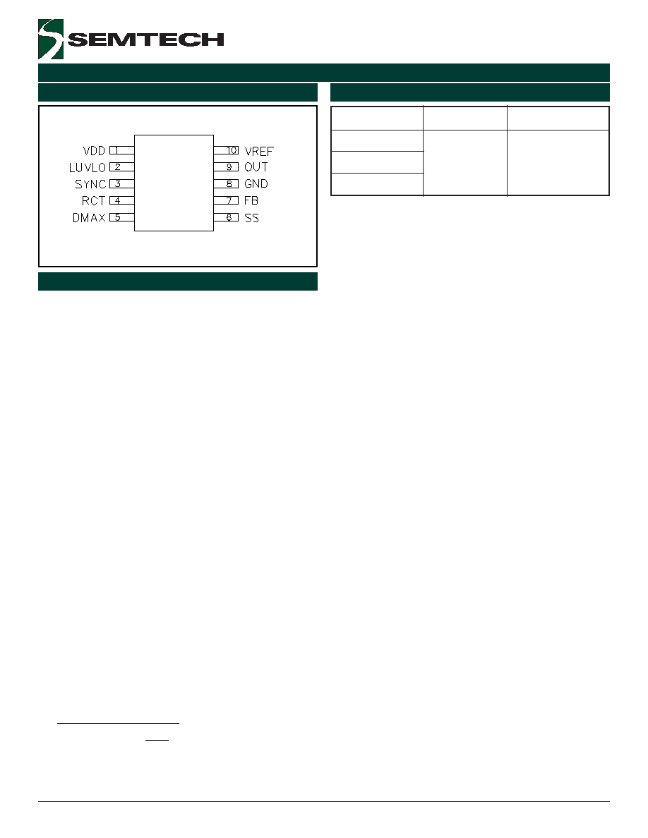
Pin Configuration
Ordering Information
Pin Descriptions
FB: This pin is the summing node for current sense feed-
back, voltage sense feedback (by optocoupler) and slope
compensation. Slope compensation is derived from the
rising voltage at the time capacitor and can be buffered
with an external small signal NPN transistor. External
high frequency filter capacitance applied from this node
to GND is discharged by an internal 250
on-resistance
NMOS FET during PWM off -time and offers effective lead-
ing edge blanking set by the RC time constant of the
feedback resistance from the current sense resistor to
the FB input and the high frequency filter capacitor ca-
pacitance at this node to GND.
GND: Reference ground and power ground for all func-
tions.
OUT: This pin is the logic level drive output to the exter-
nal MOSFET driver circuit (similar to SC1301).
VREF: The internal 4V (A) / 5V (B & C) reference output.
This reference is buffered and is available on the VREF
pin. VREF should be bypassed with a 0.47 - 1.0µF ce-
ramic capacitor.
RCT: The oscillator frequency is configured by connect-
ing resistor RT from VREF to RCT and capacitor CT from
RCT to ground. Using the equation below values for RT
and CT can be selected to provide the desired OUT fre-
quency.
-
∑
∑
-
=
-
REF
K
P
V
V
1
ln
CT
RT
1
F
where V
P-K
= RCT peak voltage
DMAX: Duty cycle up to 98% can be programmed via R4
and R5 (the resistor divider from Vref in the Application
Circuit). When DMAX pin is taken above 3V, 100% duty
cycle is achieved.
SS: This pin serves two functions. The soft start timing
capacitor connects to SS and is charged by an internal
8µA current source. Under normal soft start SS is dis-
charged to less than 1V and then ramps positive to 1V
during which time the output driver is held low. As SS
charges from 1V to 2V, soft start is implemented by an
increasing output duty cycle. If SS is taken below shut-
down threshold, the output driver is inhibited and held
low. The user accessible voltage reference also goes
low and IDD < 100µA.
VDD: The power input connection for this device. This pin
is shunt regulated at 17.5V which is sufficiently below the
voltage rating of the DMOS output driver stage. VDD
should be bypassed with a 1µF ceramic capacitor.
LUVLO: Line undervoltage lock out pin. An external resis-
tive divider will program the undervoltage lock out level.
During the LUVLO, the Driver outputs are disabled and
the softstart is reset.
SYNC: SYNC is a positive edge triggered input with a
threshold set to 2.1V. In the Bi-Phase operation mode
the SYNC pin should be connected to the CT
(Timing Capacitor) of the second controller. This will force
a out of phase operation. In a single controller opera-
tion, SYNC could be grounded or connected to an exter-
nal synchronization clock with a frequency higher than
the on-board oscillator frequency. The external OSC fre-
quency should be 30% greater for guaranteed SYNC
operation.
MSOP-10
Note:
Only available in tape and reel packaging. A reel
contains 2500 devices.
r
e
b
m
u
N
t
r
a
P
e
g
a
k
c
a
P
T
(
e
g
n
a
R
.
p
m
e
T
J
)
R
T
S
M
I
A
9
0
8
4
C
S
0
1
-
P
O
S
M
C
∞
0
5
1
+
o
t
C
∞
0
4
-
R
T
S
M
I
B
9
0
8
4
C
S
R
T
S
M
I
C
9
0
8
4
C
S
Top View

5
2003 Semtech Corp.
www.semtech.com
SC4809A/B/C
POWER MANAGEMENT
Block Diagram
Marking Information
Part Number (Example: 1456)
yyww = Datecode (Example: 0012)
xxxxx = Semtech Lot # (Example: E901
xxxxx = 01-1)
Top Mark
Bottom Mark
xxxx
xxxx
Top Mark
Bottom Mark
xxxx
xxxx
Top Mark
Bottom Mark
yyww
AF0C
xxxx
xxxx
yyww
AF0A
yyww
AF0B

6
2003 Semtech Corp.
www.semtech.com
SC4809A/B/C
POWER MANAGEMENT
Applications Information
Flyback, 90V - 300V to 5V @ 1A typ.
VCC
3
OUT
4
IN
1
EN
5
GND
2
U2
SC1301A
U4
SC4431
Q3
IRFR420
R12 2.2
T1
U3
MOC207
R16
150
C18
330/6.3V/0.04 Ohm
R18
3k
R15
1.5
C16
2.7n
R20
316
D2
US1G
Np1
Np2
Ns1
C14
220pF
VDD
1
LUVLO
2
SYNC
3
FB
7
GND
8
OUT
9
VREF
10
DMAX
5
SS
6
RCT
4
U1
SC4809
R21
102
C17 1n
5
11
2
6
71
R19 10k
R14
100
L2
10uH
C20
0.1
C19
10uF/6.3V
D3
US1B
D4
B240
R5
510
Z2
CMZ5929
C5
0.1
C9
33n
R13
300
R8 4.3k
R9 5.6k
R7 7.5k
R11
3k
R10
1k
R6
10k
R4
100k
C7
100p
Q2
FMMT718
C8
0.1
C6
100p
R3 820k
R2
2M
C10 1n
C12 0.1
C21
2.2n
L1
(Opt.)
C3 2.2n
C2 2.2n
C1
1/450V
90 - 300VDC
Q1 FZT458
Z1
BZX84C12
D1 SD103C
R1
750k
C4
47/400V
Z3
SMBJ85
+
_
C13
4.7/20V/1.8 Ohm
C11 0.33
T1
-----------------------------------------
Core: EFD15, 3C85
Magnetizing L = 230uH
Np1 = 24 ts
Np2 = 5 ts
Ns1 = 2 ts
Approximate Gap = 0.038mm
AL value = 397 nH/N≤
Fsw = 500kHz
Vcc
Q3: IRFR420, Dpak, Inter.Rect.
B240, SMB, Vishay
C17: 6TPB330M, "7343", Sanyo
U1: SC4809AIMSTR, MSOP-10, SEMTECH
U2: SC1301AISKTR, SOT-23-5, SEMTECH
U4: SC4431CSK, SOT-23-5, SEMTECH
CRITICAL COMPONENTS:
L2: TOKO, A920CY-100M or similar
C15
0.1
R17
1k
5V@1A
7
2003 Semtech Corp.
www.semtech.com
SC4809A/B/C
POWER MANAGEMENT
Application Information
The flyback power stage is very popular in 48V input
telecom applications for output power levels up to
approximately 50 watts. The exact power rating of the
flyback power stage, of course, is dependent on the input
voltage/output voltage combination, its operating
environment and many other factors. Additional output
voltages can be generated easily by simply adding another
winding to the coupled inductor along with an output
diode and output capacitor. Obtaining multiple output
voltages from a single power stage is another advantage
of the flyback power stage.
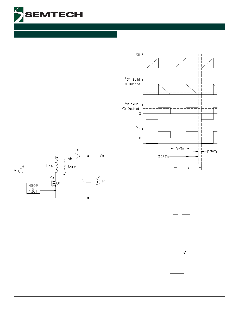
A simplified schematic of the flyback power stage with a
drive circuit block included is shown in Figure 1. In the
schematic shown, the secondary winding of the coupled
inductor is connected to produce output voltage. The
power switch, Q1, is an N-channel MOSFET. The
secondary inductance, L
SEC
and capacitor C, make up the
output filter, The resistor R, represents the load seen by
the power supply output.
Figure 1: Flyback Power Converter
The important waveforms of the flyback power stage
operating in DCM are shown in Figure 2.
Figure 2: Discontinuous Mode Flyback Waveforms
The simplified voltage conversion relationship for the
flyback power stage operating in CCM is given by:
D
1
D
N
N
V
V
P
S
I
O
-
∑
∑
=
The simplified voltage conversion relationship for the
flyback power stage operating in DCM is given by:
K
D
N
N
V
V
P
S
I
O
∑
∑
=
Where K is defined as:
S
SEC
T
R
L
2
K
∑
∑
=
8
2003 Semtech Corp.
www.semtech.com
SC4809A/B/C
POWER MANAGEMENT
Control-to-Output transfer function for the flyback power
stage operating in CCM is given by:
2
O
2
O
2
z
1
z
P
S
2
I
O
S
Q
S
1
S
1
S
1
N
N
)
D
1
(
V
dD
dV
+
∑
+
-
∑
+
∑
∑
-
=
where:
C
L
R
x
)
D
1
(
Q
C
L
D
1
L
D
R
)
D
1
(
C
R
1
1
z
SEC
SEC
O
SEC
2
2
z
C
-
∑
-
∑
∑
-
∑
=
Control-to Output transfer function for the flyback power
stage operating in DCM is given by:
P
SEC
S
P
S
I
O
S
1
1
L
2
T
R
N
N
V
dD
dV
+
∑
∑
∑
∑
∑
=
where:
C
R
2
P
∑
=
Peak current mode control requires simpler
compensation, has pulse-by-pulse current limiting, and
has better load current regulation. Primary and secondary
RMS currents can be up to two times higher for
discontinuous mode than for CCM. Discontinuous
conduction mode would require using a transistor with a
higher current rating. Because the output ripple current
is less than it would be continuous mode were used, the
output capacitors are smaller. Continuous conduction
mode (CCM) was therefore chosen.
Application Information (Cont.)
The DC transfer function of a CCM flyback converter is:
-
∑
=
-
+
max
max
)
on
(
Rds
(min)
IN
D
O
D
1
D
N
1
V
V
V
V
where V
O
= output voltage,
V
D
= forward voltage drop across rectifier D1,
N = turns ratio, equal to N
P
/N
S
,
D = duty cycle.
Transformer Design
The transformer in a flyback converter is actually a coupled
inductor with multiple windings. Transformers provide
coupling and isolation whereas inductors provide energy
storage. The energy stored in the air gap of the inductor
is equal to:
(
)
2
I
L
E
2
PEAK
P
∑
=
where E is in Joules, L
P
is the primary inductance in
Henries, and I
PEAK
is the primary peak current in Amperes.
When the switch is on, D1 is reverse biased due to the
dot configuration of the transformer. No current flows in
the secondary windings and the current in the primary
winding ramps up at a rate of:
P
)
on
(
Rds
(min)
IN
L
L
V
V
t
I
-
=
The output capacitor, C
OUT
, supplies all of the load current
at this time. Because the converter is operating in the
continuous conduction mode,
I
L
is the change in the
inductor current which appears as a positive slope ramp
on a step. The step is present because there is still
current left in the secondary windings when the primary
turns on. When the switch turns off, current flows through
the secondary winding and D1 as a negative ramp on a
step, replenishing C
OUT
and supplying current directly to
the load.

9
2003 Semtech Corp.
www.semtech.com
SC4809A/B/C
POWER MANAGEMENT
The primary inductance can be calculated given an
acceptable current ripple,
I
L
.
I
L
was set to equal one-
half the peak primary current. For a CCM flyback design,
the peak primary current is calculated:
2
I
D
1
1
N
I
I
L
max
(max)
OUT
PEAK
+
-
∑
=
Because the converter is operating in the continuous
mode, the maximum peak flux density B
MAX
, is limited by
the saturation flux density, B
SAT
. Taking all this into
consideration, the maximum core size is determined by.
31
.
1
MAX
4
RMS
PEAK
P
B
k
420
10
I
I
L
AP
∑
∑
∑
∑
∑
=
where AP = the core area product in cm
4
,
k = winding factor,
B
MAX
B
SAT
,
The result is compared to the product of the winding area,
Aw (cm
2
), and effective core area, Ae (cm
2
), listed in the
core manufacturer's data sheet.
The minimum number of primary turns is determined by:
Ae
B
10
I
L
N
MAX
4
PEAK
P
P
∑
∑
∑
=
Based upon this result and the predetermined turns ratio,
the number of secondary turns is established.
The energy stored in the flyback transformer is actually
stored in an air gap in the core. This is because the high
permeability of the ferrite material can't store much
energy without saturating first. By adding an air gap, the
hysteresis curve of the magnetic material is actually tilted,
requiring a much higher field strength to saturate the
core. The length of the air gap is calculated by:
P
2
2
P
r
o
g
L
10
Ae
)
N
(
-
∑
∑
∑
µ
∑
µ
=
l
Application Information (Cont.)
MOSFET Selection
The switching element in a flyback converter must have
a voltage rating high enough to handle the maximum input
voltage and the reflected secondary voltage, not to
mention any leakage inductance induced spike that is
inevitably present. Approximate the required voltage
rating of the MOSFET using.
(
)
(
)
3
.
1
V
V
N
N
V
V
V
D
O
S
P
L
(max)
IN
ds
∑
+
∑
+
+
=
where V
ds
= the required drain to source voltage rating of
the MOSFET,
V
L
= the voltage spike due to the leakage inductance of
the transformer, estimated to be thirty percent of V
IN(MAX)
,
and the additions 1.3 factor includes an overall thirty
percent margin.
This FET will experience both switching and conduction
losses. The conduction losses will be equal to the I
2
R
losses, as shown by:
( )
)
ON
(
DS
2
RMS
COND
R
I
P
∑
=
Switching losses are the result of overlapping drain
current and drain to source voltage at turn on and turn
off.
The total switching losses are estimated based on
equation:
sw
ch
PEAK
DS
SW
2
DS
OSS
SW
f
t
I
V
2
f
)
V
(
C
P
∑
∑
∑
+
∑
∑
=
where t
ch
:
)
th
(
gs
g
gd
CH
V
VDD
R
Q
t
-
∑
=
Diode Selection
Schottky rectifiers have a lower forward voltage drop than
typical PN devices, making it the rectifier of choice when
considering reducing converter losses and improving
overall efficiency. Selecting the appropriate Schottky for
a specific application depends mainly on the working
peak reverse voltage rating and peak repetitive forward
current.

10
2003 Semtech Corp.
www.semtech.com
SC4809A/B/C
POWER MANAGEMENT
Input and Output Capacitors
The input capacitors are chosen based upon their ripple
current rating and their rated voltage. The actual capacitor
value is not that critical as long as the minimum
capacitance gives an acceptable ripple voltage
determined by the following equation:
V
f
8
I
C
SW
RMS
MIN
∑
∑
=
The output capacitors are also chosen based upon their
low equivalent series resistance (ESR), ripple current and
voltage ratings. The ripple current that the output
capacitor experiences is a result of supplying the load
current during the FET conduction time and its charging
current during the FET off-time.
Voltage Feedback
The FB pin of the SC4809 sums the voltage feedback
signal to the current sense signal and any added slope
compensation. The voltage feedback signal is from an
optocoupler, which is driven from an error amplifier on
the secondary side of the converter. The signal from the
optocoupler is designed to trip the FB threshold of the
SC4809 internal comparator when the output voltage
exceeds its specified limit.
Current Limit
Selection of the current sense resistor is accomplished
by dividing the FB threshold value by the peak primary
current at the desired current limit point. This ground-
referenced R
SENSE
must be a low inductance type and have
a rated power level to meet the (I
RMS
)
2
∑
R
SENSE
requirement.
Current spikes caused by the leakage inductance of the
flyback transformer and the reverse recovery of the diode
could trip the current sense latch and prematurely shut
off the output. This unwanted spike can be suppressed
by adding a small RC filter for effective leading edge
blanking.
Slope Compensation
Sensing peak inductor current instead of average
inductor current results in a loop response that is Less
than ideal. Adding slope compensation to the current
signal cancels this error by maintaining a constant average
current independent of duty cycle. Slope compensation
is required for open loop stability in a current mode system
with 50% or greater duty cycles, but will benefit any
current mode application at the cost of a few small parts.
Loop Compensation
The continuous current mode flyback will contain a right-
half-plane (RHP) zero in its transfer function. Any increase
in load current will require the primary peak inductor
current to increase. The duty cycle must increase to
accomplish this. In a flyback converter, the inductor
current flows to the output only when the FET is off and
the diode is conducting. Increasing the duty cycle
increases the FET condition time but decreases the diode
conduction time. The result of this is the average diode
current, the current that supplies the load, actually
decreases. This is a temporary situation; as the inductor
current rises, the diode current eventually reaches its
proper value. The condition where the average diode
current must actually decrease before it can increase is
referred to as a right-half-plane zero. To complicate
matters, this zero contributes a phase lag, not a phase
lead as a normal zero would. This zero moves in frequency
as a function of load and input voltage, making it
impossible to cancel out by the insertion of a pole.
)
V
N
V
(
L
R
2
V
N
f
OUT
IN
P
OUT
2
IN
RHPZERO
∑
+
∑
∑
∑
∑
∑
=
The easiest way to deal with a right-half-plane zero is to
roll off the loop gain at a relatively low frequency using
simple dominant pole compensation. Unfortunately, the
result of this is poor dynamic response.
The primary goal of the compensation network is to
provide good line and load regulation and dynamic
response. These objectives are best met by providing
high gain at low frequencies for good DC regulation and
high bandwidth for good transient response. Optimum
closed loop performance can only be achieved by first
Application Information (Cont.)
11
2003 Semtech Corp.
www.semtech.com
SC4809A/B/C
POWER MANAGEMENT
knowing what the transfer characteristic of the PWM and
switching circuit looks like. Constructing a Bode plot of
the known poles and zeros in the power stage does this.
Bode plots give a visual interpretation of the gain versus
frequency and phase versus frequency characteristics
of a system. In the gain plot, the gain shown at each
frequency represents the amount by which the feedback
loop will reduce a disturbance at that frequency.
Besides the RHP zero, the output capacitor and the load
contribute a pole and the output capacitor alone will
contribute a zero based upon its ESR.
OUT
OUT
pole
C
R
2
D
1
f
∑
∑
∑
+
=
OUT
zero
C
ESR
2
1
f
∑
∑
=
The control to output gain is calculated by:
+
∑
∑
∑
-
∑
∑
∑
∑
∑
=
)
V
V
N
2
(
)
D
1
(
V
V
R
I
log
20
GAIN
IN
O
C
IN
OUT
SC
Once the frequency response of the uncompensated
system is determined, the next step is to determine what
compensation is needed around the error amplifier for
optimum performance. As stated earlier, optimum
performance requires a high gain at low frequencies for
good DC regulation and high bandwidth for good transient
response. The crossover frequency, f
c
, is the frequency
at which the gain magnitude equals 0dB. High bandwidth
is achieved by having the highest possible f
c
. Because of
the RHP zero, the highest possible crossover frequency
is limited to f
RHPZERO
/
. The phase margin, or the amount
the phase lag measures at f
c
less 180∞, should be at
least 45∞ for good transient response with little
overshoot. The magnitude of the gain at the frequency
where the phase plot measures - 180∞ is referred to as
the gain margin. If the slope of the gain plot is -2, or
-40dB/decade, at low frequencies, it much transition to
a -20dB/decade slope, also known as a -1 slope, one
decade before crossing the 0dB point. If the slope
remains at the -2 slope the resultant gain margin would
be too small causing sever underdamped oscillations at
fc.
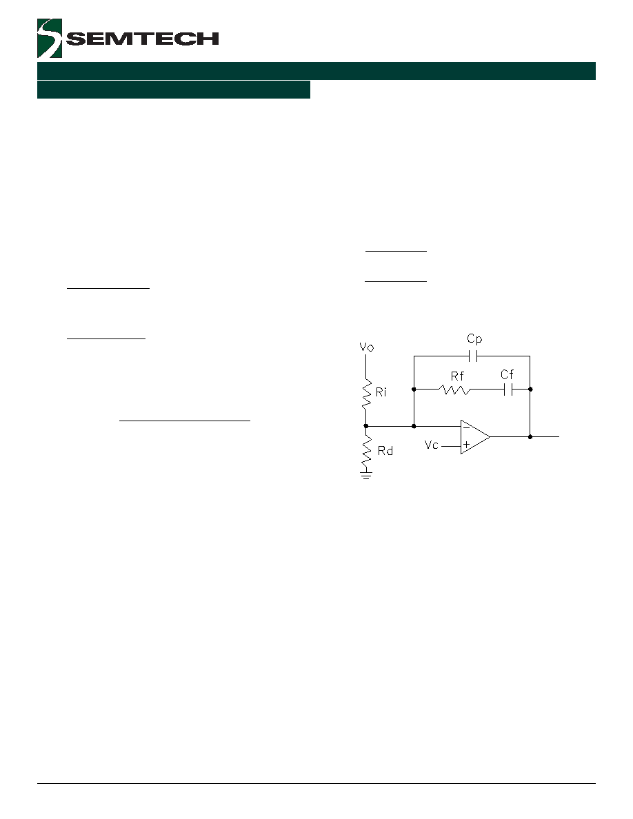
Application Information (Cont.)
The scheme shown below will handle most compensation
requirements. There is a pole at the origin which
contributes a -1 slope in the gain plot, a low frequency
zero, f
EAZERO
flattens out the slope so the mid-range gain
is equal to Rf/Ri. A high frequency pole, f
EAPOLE
helps
suppress any high frequency noise from propagating
through the system. Rd forms a voltage divider with Ri
and provides a DC offset.
p
f
EAPOLE
f
f
EAZERO
C
R
2
1
f
C
R
2
1
f
∑
∑
∑
=
∑
∑
∑
=
By combining the Bode plots of the PWM and power stage
with the error amplifier compensation, a plot of the entire
system is realized.

12
2003 Semtech Corp.
www.semtech.com
SC4809A/B/C
POWER MANAGEMENT
C1 1.0/100V
C5 0.47
C4 0.1
+48V
-- 48V
R6 10k
C2 100p
R7 1k
VCC
3
OUT
4
IN
1
EN
5
GND
2
U2
SC1301
Q2
IRF640N
R14
0.2 1/2W
R12
1k
C6
200p
R11
7.5k
R3
1k
R2
20k
D1
MURD620CT
C7 0.1
DISABLE
VDD
1
LUVLO
2
SYNC
3
FB
7
GND
8
OUT
9
VREF
10
DMAX
5
SS
6
RCT
4
U1
SC4809
L1
10uH
Q3
BSS64ZXCT
Z2 ZMM5242B
C9 1n
R15 22k
R16 47k
R17
1k
R13
10
R10
47k
R18
200 1W
C11 1.0
C10
150/16V
GND
+12V
C1 1.0/100V
C5 0.47
C4 0.1
R6 10k
C2
150p
R7 1k
VCC
3
OUT
4
IN
1
EN
5
GND
2
U2
SC1301
Q2
IRF640N
R14
0.2 1/2W
R12
1k
C6
200p
R11
7.5k
R3
1k
R2
20k
D1
MURD620CT
C7 0.1
DISABLE
VDD
1
LUVLO
2
SYNC
3
FB
7
GND
8
OUT
9
VREF
10
DMAX
5
SS
6
RCT
4
U1
SC4809
L1
10uH
Q3
BSS64ZXCT
Z2 ZMM5242B
C9 1n
R15 22k
R16 47k
R17
1k
R13 10
R10
47k
R18 200 1W
C11
1.0
C10
150/16V
GND
+12V
Z1
ZMM5242B
Z1
ZMM5242B
R9
100
C8
1.0
C8
1.0
R9
100
Qa
TIP30C
R1
1k
Rb
300 1W
Ra
300 1W
Za
ZMM5242B
C3
0.47
C3 0.47
R8
3.9k
R8
3.9k
R4
2.7k
R4
2.7k
R5
7.5k
R5
7.5k
Q1
MMBT2907A
Q1
MMBT2907A
"MASTER"
"SLAVE"
Out of Phase, Synchronized, Dual Converter
Applications Information (Cont.)
13
2003 Semtech Corp.
www.semtech.com
SC4809A/B/C
POWER MANAGEMENT
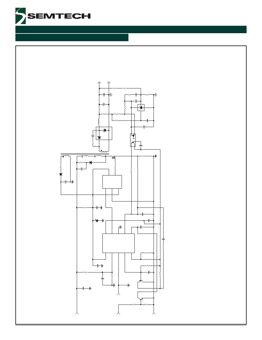
Evaluation Board Schematic
50W Forward Converter
C7
0.
47
C6
0.
033
R7
10k
C4 *
R8
1.
5k
R1
2
*
U4 SC
4431
VC
C
3
OU
T
4
IN
1
EN
5
GN
D
2
U2
S
C
1301
A
R1 5.
1k
R2 1k
Q1
M
M
BT
2222A
Q3
I
R
F
6
40NS
R1
5
3.
3
R1
8
*
R1
7
*
C8
*
U3
M
O
C
207
R1
6
*
R4
10k
R3
100k
R2
1
1k
C9
1/
25V
C1
7
10.
0
D3
M
B
R
B
1530C
T
C1
4
-
1
6
470/
6.
3V
C2
0
430p
F
R2
4
1.
21k
R2
2
39.
2
k
R2
5
3.
83k
R6
2
k
R1
0
*
C5 0.
01
SYN
C
C1
2
220p
F
C1
0
1.
0/
16V
C1
1
0.
01/
1
00V
R1
4
3.
3k
1W
D2
ES
1
D
R1
9
20
1/
4
W
C1
3
1n
F
/
50V
R2
3
62k
R2
6
0
SM
A
C1
1.
0/
100V
VD
D
1
LU
V
L
O
2
SYN
C
3
FB
7
GN
D
8
OU
T
9
VR
E
F
10
DM
A
X
5
SS
6
RC
T
4
U1
S
C
4
8
0
9
_A
_B
_C
1
2
7
5
6
3
6
10,
1
1
,
12
7,
8,
9
5
1
C3
0.
1/
25V
R9 7.
5k
Q2
M
M
BT
2907A
2
4
L1 2.
5u
H
@
10A
R1
1
100
C2
1
0.
01
Z1
Z
M
M
5245B
C2
0.
01
R5 10k
T
1
:
P
A
0273,
P
u
l
s
e
E
n
g
.
L
1
:
E
T
Q
P
6F2
R
5S
F
A
,
P
a
na
so
ni
c
C
1
4
-
16:
6T
P
B
470M
,
P
o
s
C
a
p
,
S
a
n
y
o
R2
0
1k
Vc
c
C1
9
0.
01
C1
8
0.
022
F
s
w
=33
0k
Hz
R10
R
16
R17
R
18
C
4
C
8
A
B
C
10
k
10
k
8.
2k
10
0
62
62
60
4
60
4
1k
0.
15
0.
15
0.
22
20
0p
30
0p
30
0p
68
0p
68
0p
39
0p
R12
2x
1
0
k
|
|
3x
1
2
k
|
|
2x
1
2
k
|
|
14
2003 Semtech Corp.
www.semtech.com
SC4809A/B/C
POWER MANAGEMENT
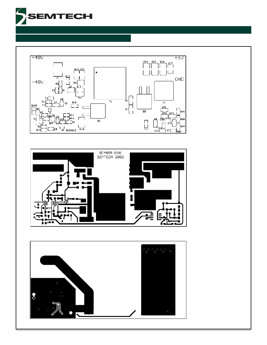
Evaluation Board Layout
50W Forward Converter
Layout
Top
Bottom
15
2003 Semtech Corp.
www.semtech.com
SC4809A/B/C
POWER MANAGEMENT
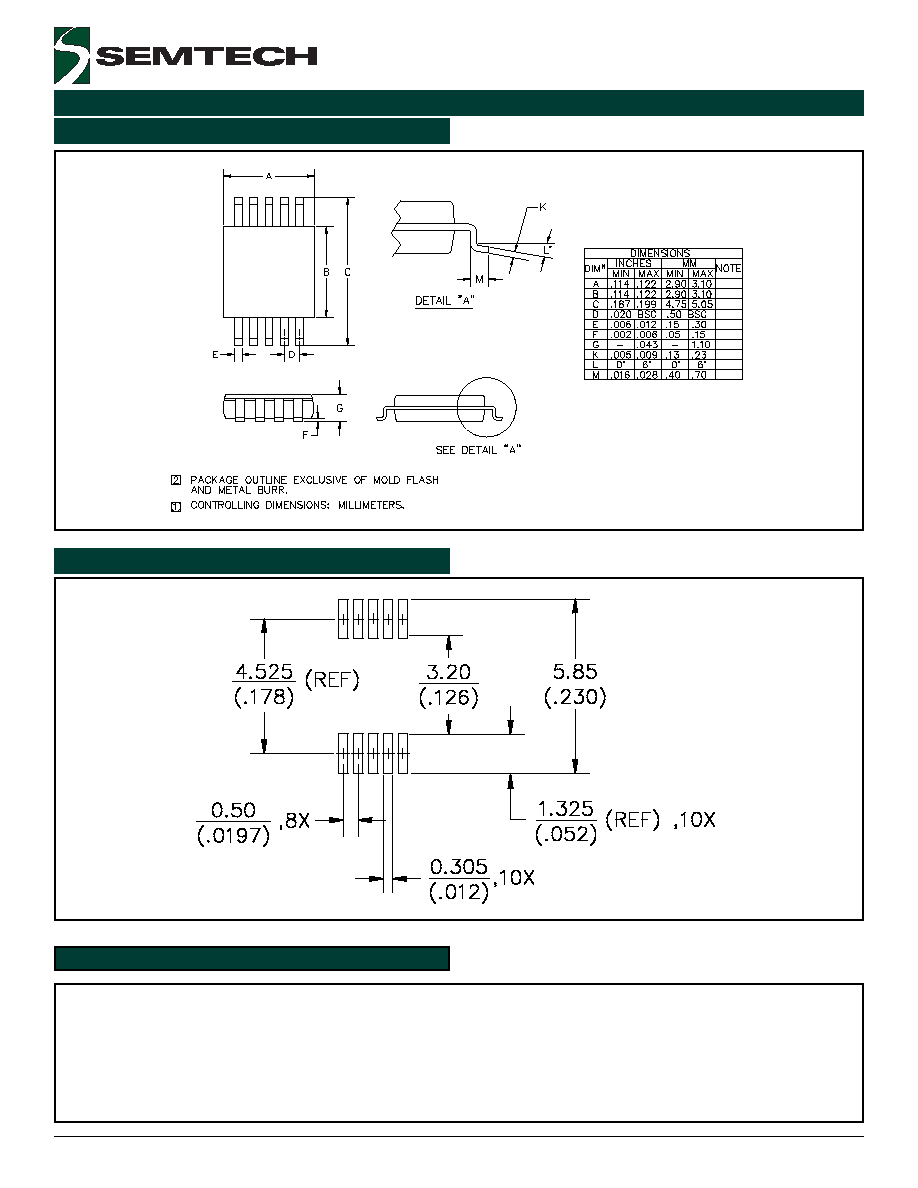
Outline Drawing - MSOP-10
Semtech Corporation
Power Management Products Division
200 Flynn Road, Camarillo, CA 93012
Phone: (805)498-2111 FAX (805)498-3804
Contact Information
Land Pattern - MSOP-10