 | ÐлекÑÑоннÑй компоненÑ: SC486 | СкаÑаÑÑ:  PDF PDF  ZIP ZIP |
SC486 data sheet
1
www.semtech.com
SC486
Complete DDR1/2 Memory
Power Supply
POWER MANAGEMENT
Revision: February 07, 2005
The SC486 is a combination switching regulator and linear
source/sink regulator intended for DDR1/2 memory
systems. The switching regulator is used to generate the
supply voltage, VDDQ, for the memory system. It is a
pseudo-fixed frequency constant on-time controller
designed for high efficiency, superior DC accuracy, and
fast transient response. The linear source/sink regulator
is used to generate the memory termination voltage, VTT,
with the ability to source and sink a 3A peak current.
For the VDDQ regulator, the switching frequency is
constant until a step in load or line voltage occurs at
which time the pulse density, i.e. frequency, will increase
or decrease to counter the transient change in output or
input voltage. After the transient, the frequency will return
to steady-state operation. At lighter loads, the selectable
Power-Save Mode enables the PWM converter to reduce
its switching frequency and improve efficiency. The
integrated gate drivers feature adaptive shoot-through
protection and soft-switching.
For the VTT regulator, the output voltage tracks VREF,
which is ½ VDDQ to provide an accurate termination
voltage. The VTT output is generated from a 1.2V to VDDQ
input by a linear source/sink regulator which is designed
for high DC accuracy, fast transient response, and low
external component count. Additional features include
cycle-by-cycle current limiting, digital soft-start, power
good (all VDDQ only) and over-voltage and under-voltage
protection (VDDQ and VTT). All 3 outputs (VDDQ, VTT and
REF) are actively discharged when VDDQ is disabled,
reducing external component count and cost. The SC486
is available in a 24 pin MLPQ 4mmx4mm lead-free
package.
Notebook computers
CPU I/O supplies
Handheld terminals and PDAs
LCD monitors
Network power supplies
24 lead MLPQ (4 x 4mm) lead free package
Constant on-time controller for fast dynamic
response on VDDQ
Programmable VDDQ range - 1.5V to 3V
1% Internal Reference (2% System Accuracy)
Resistor programmable on time for VDDQ
VCCA/VDDP range = 4.5V to 5.5V
VBAT range = 2.5V to 25V
VDDQ DC current sense using low-side R
DS(ON)
sensing or external R
SENSE
in series with low-side
FET
Cycle-by-cycle current limit for VDDQ
Digital soft-start for VDDQ
Combined EN and PSAVE pin for VDDQ
Over-voltage/under-voltage fault protection for
both outputs and PGD output (VDDQ only)
Separate VCCA and VDDP supplies
VTT/REF range = 0.75V 1.5V
VTT source/sink 3A peak
Internal resistor divider for VTT/REF
VTT is high impedance in S3
VDDQ, VTT and REF are actively discharged in
S4/S5
+
C10
VDDQ
C12
1uF
C11
20uF
VTT
C9
1uF
R2
10R
5VRUN
5VSUS
C3
no-pop
R7 10R
REF
R6
10R
C6
1uF
R4 10R
C2
1uF
R5
R9
VDDQ
PGOOD
VBAT
C8
1nF
C1
no-pop
C7
no-pop
R8 0R
VDDQ
4
1
2
3
5
6
7
8
Q1
R10
C13
1uF
C4
0.1uF
D1
R3 470k
5VSUS
C5
10uF
R1
VBAT
L1
PGND1
18
REF
8
EN/PSV
1
TON
2
VDDQS
3
VCCA
5
FB
6
PGD
7
VSSA
4
PGND2
17
DL
19
VDDP
20
ILIM
21
LX
22
DH
23
BST
24
VTTEN
11
VTT
15
PGND2
16
VTTIN
12
VTTIN
13
VTT
14
VTTS
10
COMP
9
PA
D
U1
SC486
Description
Features
Applications
Typical Application Circuit
2
2005 Semtech Corp.
www.semtech.com
SC486
POWER MANAGEMENT
Absolute Maximum Ratings
(10)
Test Conditions: V
BAT
= 15V, VCCA = VDDP = VTTEN = EN/PSV = 5V, VDDQ = VTTIN = 1.8V, R
TON
= 1M
r
e
t
e
m
a
r
a
P
s
n
o
i
t
i
d
n
o
C
C
°
5
2
C
°
5
2
1
o
t
C
°
0
4
-
s
t
i
n
U
n
i
M
p
y
T
x
a
M
n
i
M
x
a
M
s
e
il
p
p
u
S
t
u
p
n
I
t
n
e
r
r
u
C
g
n
it
a
r
e
p
O
A
C
C
V
I
,t
n
i
o
p
n
o
it
a
l
u
g
e
r
>
B
F
Q
D
D
V
A
0
=
0
0
5
1
0
0
5
2
A
µ
3
S
,t
n
e
r
r
u
C
g
n
it
a
r
e
p
O
A
C
C
V
I
,t
n
i
o
p
n
o
it
a
l
u
g
e
r
>
B
F
Q
D
D
V
,
A
0
=
V
0
=
N
E
T
T
V
0
0
0
1
A
µ
t
n
e
r
r
u
C
g
n
it
a
r
e
p
O
P
D
D
V
I
,t
n
i
o
p
n
o
it
a
l
u
g
e
r
>
B
F
Q
D
D
V
A
0
=
0
7
0
5
1
A
µ
t
n
e
r
r
u
C
g
n
it
a
r
e
p
O
N
O
T
M
1
=
N
O
T
R
5
1
A
µ
t
n
e
r
r
u
C
g
n
it
a
r
e
p
O
N
I
T
T
V
I
T
T
V
A
0
=
1
5
A
µ
N
O
T
+
P
D
D
V
+
A
C
C
V
t
n
e
r
r
u
C
n
w
o
d
t
u
h
S
V
0
=
N
E
T
T
V
=
V
S
P
/
N
E
5
1
1
A
µ
r
e
t
e
m
a
r
a
P
l
o
b
m
y
S
m
u
m
i
x
a
M
s
t
i
n
U
A
S
S
V
o
t
N
O
T
0
.
5
2
+
o
t
3
.
0
-
V
1
D
N
G
P
o
t
T
S
B
,
H
D
0
.
0
3
+
o
t
3
.
0
-
V
1
D
N
G
P
o
t
X
L
0
.
5
2
+
o
t
0
.
2
-
V
1
D
N
G
P
o
t
P
D
D
V
,
M
I
L
I
,
L
D
0
.
6
+
o
t
3
.
0
-
V
L
D
o
t
P
D
D
V
0
.
6
+
o
t
3
.
0
-
V
2
D
N
G
P
o
t
T
T
V
,
N
I
T
T
V
0
.
6
+
o
t
3
.
0
-
V
T
T
V
o
t
N
I
T
T
V
0
.
6
+
o
t
3
.
0
-
V
,
N
E
T
T
V
,
S
Q
D
D
V
,
A
C
C
V
,
F
E
R
,
D
G
P
,
B
F
,
V
S
P
/
N
E
,
P
M
O
C
A
S
S
V
O
T
S
T
T
V
0
.
6
+
o
t
3
.
0
-
V
,
N
E
T
T
V
,
T
T
V
,
S
Q
D
D
V
,
F
E
R
,
B
F
,
V
S
P
/
N
E
,
P
M
O
C
o
t
A
C
C
V
S
T
T
V
,
N
I
T
T
V
0
.
6
+
o
t
3
.
0
-
V
A
S
S
V
o
t
1
D
N
G
P
,
2
D
N
G
P
o
t
1
D
N
G
P
3
.
0
+
o
t
3
.
0
-
V
X
L
o
t
H
D
,
T
S
B
0
.
6
+
o
t
3
.
0
-
V
t
n
e
i
b
m
A
o
t
n
o
it
c
n
u
J
e
c
n
a
t
s
i
s
e
R
l
a
m
r
e
h
T
A
J
6
4
W
/
C
°
e
g
n
a
R
e
r
u
t
a
r
e
p
m
e
T
n
o
it
c
n
u
J
g
n
it
a
r
e
p
O
T
J
0
5
1
+
o
t
0
4
-
C
°
e
g
n
a
R
e
r
u
t
a
r
e
p
m
e
T
e
g
a
r
o
t
S
T
G
T
S
0
5
1
+
o
t
5
6
-
C
°
s
0
4
-
s
0
1
,
e
r
u
t
a
r
e
p
m
e
T
w
o
lf
e
R
R
I
k
a
e
P
T
G
K
P
0
6
2
C
°
Exceeding the specifications below may result in permanent damage to the device, or device malfunction. Operation outside of the parameters
specified in the Electrical Characteristics section is not implied. Exposure to Absolute Maximum rated conditions for extended periods of time may
affect device reliability.
Electrical Characteristics
3
2005 Semtech Corp.
www.semtech.com
SC486
POWER MANAGEMENT
r
e
t
e
m
a
r
a
P
s
n
o
i
t
i
d
n
o
C
C
°
5
2
C
°
5
2
1
o
t
C
°
0
4
-
s
t
i
n
U
n
i
M
p
y
T
x
a
M
n
i
M
x
a
M
r
e
ll
o
r
t
n
o
C
Q
D
D
V
d
l
o
h
s
e
r
h
T
r
o
t
a
r
a
p
m
o
C
r
o
r
r
E
B
F
)
1
(
V
5
.
5
o
t
V
5
.
4
=
A
C
C
V
0
0
5
.
1
5
8
4
.
1
5
1
5
.
1
V
e
m
i
T
-
n
O
R
N
O
T
M
1
=
V
8
.
1
=
Q
D
D
V
,
0
6
4
0
9
3
0
3
5
s
n
R
N
O
T
k
0
0
5
=
V
8
.
1
=
Q
D
D
V
,
5
6
2
5
2
2
5
0
3
e
m
i
T
-
ff
O
m
u
m
i
n
i
M
0
0
4
0
5
5
s
n
e
c
n
a
t
s
i
s
e
R
t
u
p
n
I
S
Q
D
D
V
0
5
1
k
n
w
o
d
t
u
h
S
S
Q
D
D
V
e
c
n
a
t
s
i
s
e
R
e
g
r
a
h
c
s
i
D
D
N
G
=
V
S
P
/
N
E
2
2
t
n
e
r
r
u
C
e
g
a
k
a
e
L
B
F
0
.
1
-
0
.
1
A
µ
r
e
ll
o
r
t
n
o
C
T
T
V
t
n
e
r
r
u
C
e
g
a
k
a
e
L
P
M
O
C
0
.
1
-
0
.
1
A
µ
t
n
e
r
r
u
C
e
c
r
u
o
S
F
E
R
0
1
A
m
y
c
a
r
u
c
c
A
t
u
p
t
u
O
F
E
R
I
F
E
R
A
m
0
1
o
t
0
=
0
0
9
2
8
8
8
1
9
V
m
n
w
o
d
t
u
h
S
F
E
R
e
c
n
a
t
s
i
s
e
R
e
g
r
a
h
c
s
i
D
D
N
G
=
V
S
P
/
N
E
2
2
y
c
a
r
u
c
c
A
t
u
p
t
u
O
T
T
V
I
<
A
2
-
T
T
V
A
2
<
F
E
R
0
2
-
0
2
+
V
m
n
w
o
d
t
u
h
S
T
T
V
e
c
n
a
t
s
i
s
e
R
e
g
r
a
h
c
s
i
D
D
N
G
=
V
S
P
/
N
E
2
2
t
n
e
r
r
u
C
e
g
a
k
a
e
L
S
T
T
V
0
.
1
-
0
.
1
A
µ
g
n
i
s
n
e
S
t
n
e
r
r
u
C
t
n
e
r
r
u
C
M
I
L
I
0
1
9
1
1
A
µ
t
e
s
ff
O
r
o
t
a
r
a
p
m
o
C
t
n
e
r
r
u
C
M
I
L
I
-
1
D
N
G
P
0
1
-
0
1
V
m
d
l
o
h
s
e
r
h
T
g
n
i
s
s
o
r
C
-
o
r
e
Z
V
5
=
V
S
P
/
N
E
,
X
L
-
1
D
N
G
P
5
V
m
n
o
i
t
c
e
t
o
r
P
t
l
u
a
F
Q
D
D
V
)
e
v
it
i
s
o
P
(
ti
m
i
L
t
n
e
r
r
u
C
)
2
(
R
,
X
L
-
1
D
N
G
P
M
I
L
I
k
5
=
0
5
5
3
5
6
V
m
R
,
X
L
-
1
D
N
G
P
M
I
L
I
k
0
1
=
0
0
1
0
8
0
2
1
R
,
X
L
-
1
D
N
G
P
M
I
L
I
k
0
2
=
0
0
2
0
7
1
0
3
2
)
e
v
it
a
g
e
N
(
ti
m
i
L
t
n
e
r
r
u
C
X
L
-
1
D
N
G
P
5
2
1
-
0
6
1
-
0
9
-
V
m
tl
u
a
F
e
g
a
tl
o
V
r
e
d
n
U
t
u
p
t
u
O
e
c
n
e
r
e
f
e
r
l
a
n
r
e
t
n
i
o
t
t
c
e
p
s
e
r
h
ti
W
0
3
-
5
3
-
5
2
-
%
y
a
l
e
D
tl
u
a
F
e
g
a
tl
o
V
r
e
d
n
U
h
t
V
V
U
w
o
l
e
b
d
e
c
r
o
f
B
F
8
s
k
l
c
)
3
(
e
m
i
T
k
n
a
l
B
e
g
a
tl
o
V
r
e
d
n
U
h
g
i
h
N
E
m
o
r
F
0
4
4
s
k
l
c
)
3
(
Test Conditions: V
BAT
= 15V, VCCA = VDDP = VTTEN = EN/PSV = 5V, VDDQ = VTTIN = 1.8V, R
TON
= 1M
Electrical Characteristics (Cont.)
4
2005 Semtech Corp.
www.semtech.com
SC486
POWER MANAGEMENT
r
e
t
e
m
a
r
a
P
s
n
o
i
t
i
d
n
o
C
C
°
5
2
C
°
5
2
1
o
t
C
°
0
4
-
s
t
i
n
U
n
i
M
p
y
T
x
a
M
n
i
M
x
a
M
)
.
t
n
o
C
(
n
o
i
t
c
e
t
o
r
P
t
l
u
a
F
Q
D
D
V
tl
u
a
F
e
g
a
tl
o
V
r
e
v
O
t
u
p
t
u
O
e
c
n
e
r
e
f
e
r
l
a
n
r
e
t
n
i
o
t
t
c
e
p
s
e
r
h
ti
W
6
1
+
2
1
+
0
2
+
%
y
a
l
e
D
tl
u
a
F
e
g
a
tl
o
V
r
e
v
O
h
t
V
V
O
e
v
o
b
a
d
e
c
r
o
f
B
F
5
s
µ
e
g
a
tl
o
V
t
u
p
t
u
O
w
o
L
D
G
P
A
m
1
k
n
i
S
4
.
0
V
t
n
e
r
r
u
C
e
g
a
k
a
e
L
D
G
P
V
5
=
D
G
P
,
n
o
it
a
l
u
g
e
r
n
i
B
F
1
A
µ
d
l
o
h
s
e
r
h
T
V
U
D
G
P
e
c
n
e
r
e
f
e
r
l
a
n
r
e
t
n
i
o
t
t
c
e
p
s
e
r
h
ti
W
0
1
-
2
1
-
8
-
%
y
a
l
e
D
tl
u
a
F
D
G
P
w
o
d
n
i
w
D
G
P
e
d
i
s
t
u
o
d
e
c
r
o
f
B
F
5
s
µ
e
g
a
tl
o
V
r
e
d
n
U
A
C
C
V
V
m
0
0
1
s
i
s
e
r
e
t
s
y
h
,
e
g
d
e
g
n
i
s
i
R
0
.
4
7
.
3
3
.
4
V
n
o
i
t
c
e
t
o
r
P
t
l
u
a
F
T
T
V
tl
u
a
F
e
g
a
tl
o
V
r
e
d
n
U
t
u
p
t
u
O
F
E
R
t
r
/
w
T
T
V
2
1
-
6
1
-
8
-
%
tl
u
a
F
e
g
a
tl
o
V
r
e
v
O
t
u
p
t
u
O
F
E
R
t
r
/
w
T
T
V
2
1
+
8
+
6
1
+
%
y
a
l
e
D
n
w
o
d
t
u
h
S
tl
u
a
F
w
o
d
n
i
w
V
O
/
V
U
e
d
i
s
t
u
o
T
T
V
0
5
s
µ
n
w
o
d
t
u
h
S
l
a
m
r
e
h
T
)
5
(
)
4
(
0
6
1
0
5
1
0
7
1
C
°
s
t
u
p
t
u
O
/
s
t
u
p
n
I
e
g
a
tl
o
V
w
o
L
t
u
p
n
I
c
i
g
o
L
w
o
l
V
S
P
&
N
E
2
.
1
V
w
o
l
N
E
T
T
V
6
.
0
e
g
a
tl
o
V
h
g
i
H
t
u
p
n
I
c
i
g
o
L
w
o
l
V
S
P
,
h
g
i
h
N
E
2
.
1
4
.
2
V
h
g
i
h
N
E
T
T
V
4
.
2
e
g
a
tl
o
V
h
g
i
H
t
u
p
n
I
c
i
g
o
L
h
g
i
h
V
S
P
,
h
g
i
h
N
E
4
.
2
V
e
c
n
a
t
s
i
s
e
R
t
u
p
n
I
V
S
P
/
N
E
g
n
i
c
r
u
o
S
5
.
1
M
g
n
i
k
n
i
S
0
.
1
t
r
a
t
S
t
f
o
S
e
m
i
T
p
m
a
R
t
r
a
t
S
tf
o
S
Q
D
D
V
h
g
i
h
D
G
P
o
t
h
g
i
h
V
S
P
/
N
E
0
4
4
s
k
l
c
)
3
(
e
t
a
R
p
m
a
R
t
r
a
t
S
tf
o
S
T
T
V
)
6
(
6
s
µ
/
V
m
s
e
v
i
r
D
e
t
a
G
y
a
l
e
D
n
o
it
c
e
t
o
r
P
u
r
h
t
-
t
o
o
h
S
)
7
(
)
4
(
g
n
i
s
ir
L
D
r
o
H
D
0
3
s
n
e
c
n
a
t
s
i
s
e
R
n
w
o
D
-l
l
u
P
L
D
w
o
l
L
D
8
.
0
6
.
1
t
n
e
r
r
u
C
k
n
i
S
L
D
V
L
D
V
5
.
2
=
1
.
3
A
e
c
n
a
t
s
i
s
e
R
p
U
-l
l
u
P
L
D
h
g
i
h
L
D
2
4
Test Conditions: V
BAT
= 15V, VCCA = VDDP = VTTEN = EN/PSV = 5V, VDDQ = VTTIN = 1.8V, R
TON
= 1M
Electrical Characteristics (Cont.)
5
2005 Semtech Corp.
www.semtech.com
SC486
POWER MANAGEMENT
Notes:
(1) The output voltage will have a DC regulation level higher than the error-comparator threshold by 50% of the
ripple voltage.
(2) Using a current sense resistor, this measurement relates to PGND1 minus the voltage of the source on the
low-side MOSFET.
(3) clks = switching cycles, consisting of one high side and one low side gate pulse.
(4) Guaranteed by design.
(5) Thermal shutdown latches both outputs (VTT and VDDQ) off, requiring VCCA or EN/PSV cycling to reset.
(6) VTT soft start ramp rate is 6mV/µs typical unless VDDQ/2 ramp rate is slower. If this is true, VTT soft start
ramps at 6mV/µs (typ.) until it reaches VDDQ/2, and then tracks it.
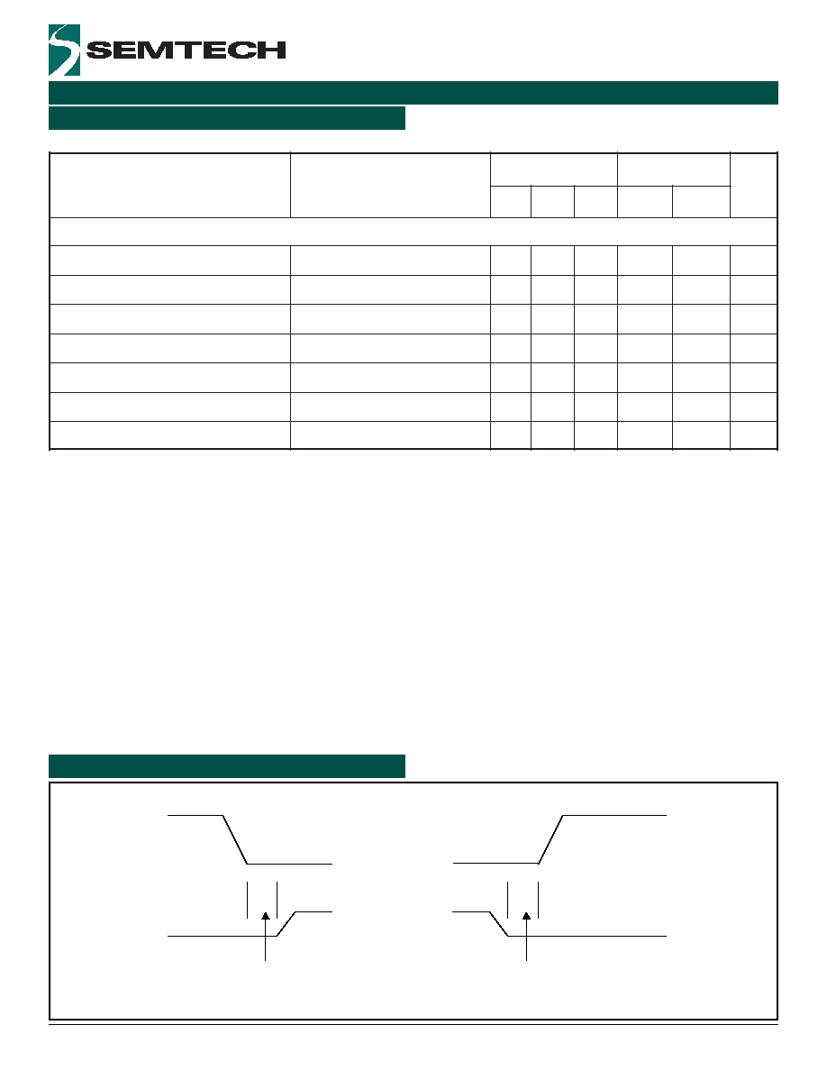
(7) See Shoot-Through Delay Timing Diagram below.
(8) Semtech's SmartDriverTM FET drive first pulls DH high with a pull-up resistance of 10
(typ.) until LX = 1.5V
(typ.). At this point, an additional pull-up device is activated, reducing the resistance to 2
(typ.). This negates the
need for an external gate or boost resistor.
(9) Provided operation below T
J(MAX)
is maintained.
(10) This device is ESD sensitive. Use of standard ESD handling precautions is required.
tplhDL
tplhDH
LX
DL
DL
DH
r
e
t
e
m
a
r
a
P
s
n
o
i
t
i
d
n
o
C
C
°
5
2
C
°
5
2
1
o
t
C
°
0
4
-
s
t
i
n
U
n
i
M
p
y
T
x
a
M
n
i
M
x
a
M
)
.
t
n
o
C
(
s
e
v
i
r
D
e
t
a
G
t
n
e
r
r
u
C
e
c
r
u
o
S
L
D
V
L
D
V
5
.
2
=
3
.
1
A
e
c
n
a
t
s
i
s
e
R
n
w
o
D
-l
l
u
P
H
D
V
5
=
X
L
-
T
S
B
,
w
o
l
H
D
2
4
e
c
n
a
t
s
i
s
e
R
p
U
-l
l
u
P
H
D
)
8
(
V
5
=
X
L
-
T
S
B
,
h
g
i
h
H
D
2
4
t
n
e
r
r
u
C
e
c
r
u
o
S
/
k
n
i
S
H
D
V
H
D
V
5
.
2
=
3
.
1
A
e
c
n
a
t
s
i
s
e
R
p
U
-l
l
u
P
T
T
V
F
E
R
<
S
T
T
V
5
2
.
0
5
4
.
0
e
c
n
a
t
s
i
s
e
R
n
w
o
D
-l
l
u
P
T
T
V
F
E
R
>
S
T
T
V
5
2
.
0
5
4
.
0
t
n
e
r
r
u
C
e
c
r
u
o
S
/
k
n
i
S
k
a
e
P
T
T
V
)
9
(
6
.
3
0
.
2
A
Test Conditions: V
BAT
= 15V, VCCA = VDDP = VTTEN = EN/PSV = 5V, VDDQ = VTTIN = 1.8V, R
TON
= 1M
Electrical Characteristics (Cont.)
Shoot-Through Delay Timing Diagram