1
www.semtech.com
SC4901
COMBI-SYNC Secondary Side
Synchronous Rectifier and Regulator
POWER MANAGEMENT
Revision Jan 2004
Description
Features
Applications
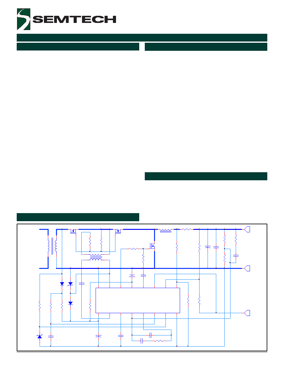
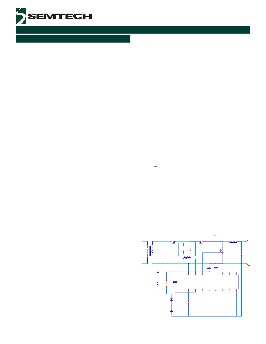
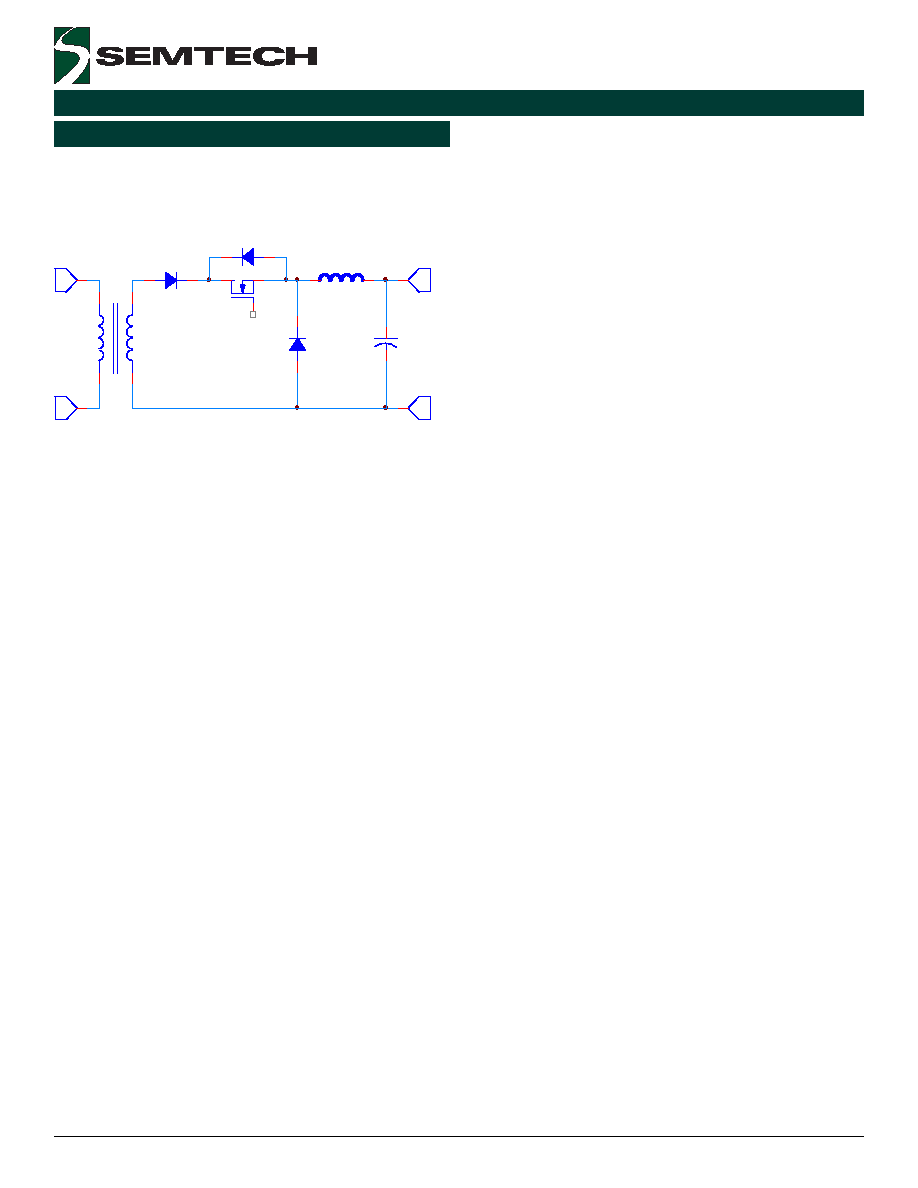
Typical Application Circuit
Single controller performs synchronous rectification
and post regulation
Independent regulation of multiple outputs from a
common secondary winding
Turn on shoot through inherently eliminated
Primary switch turns ON and OFF with zero current
No synchronising or any other signals needed across
the isolation boundary
Eliminates the need for a secondary bias supply
Independent soft start, ON/OFF, remote sense and
current limit for each output
Resistive or inductive current sensing with 2V current
signal and 2.5V reference for external applications.
4.5 to 18V operation
Max operating frequency to 1 MHz
Low profile 16 pin TSSOP package
Based on Semtech's patent pending Combi Sync
concept
SC4901 is a unique secondary side regulator designed
for implementing Semtech's proprietary Combi-Sync
topology for isolated convertors with multiple outputs. The
Combi-Sync is a true all-MOSFET topology that allows
synchronous rectification and post regulation of
transformer isolated outputs, resulting in higher efficiency
and low component count. Details of this unique topology
are described in the Application Information section.
Multiple outputs can be synchronously rectified and
independently regulated by individual SC4901s. Each
output has its own ON/OFF control, soft start, remote sense
and current limits. They can be turned on or off without
affecting the primary or other outputs. The secondary side
control makes it much easier to design tight control loops
and implement load current sharing and hot swap
features. All devices are synchronised to the transformer
winding. The current sense can be either from the output
inductor for high efficiency or a resistor for better accuracy.
An amplified current signal is provided for external use.
Each device is capable of driving high side MOSFETs with
2A current. The forward drive is configured for direct
connection to a 1:1 pulse transformer. SC4901 has an
undervoltage lockout with typical turn-on threshold of 4.5V
and is available in a low cost TSSOP-16 package
Telecom isolated DC to DC converters with multiple
low voltage outputs
High density brick and sub brick modules with
independently regulated multiple outputs
Distributed power architectures
Isolated VRMs
QS
QF
QR
D4
� �
T1
L1
C1
C9
C10
C2
C4
RZ
R13
RT
R5
R4
R8
R9
R1
R6
R7
R11
R14
R12
C7
C5
��
T2
D1
U 1
S C 4 9 0 1
ZC
D
15
CA
O
3
CS
-
2
CS
+
1
OU
T
B
6
SS
E
N
4
XF
R
A
7
PV
CC
9
PG
N
D
8
VC
C
5
AG
N
D
16
OU
T
A
10
RE
F
11
VE
A
-
12
VE
A
13
RC
T
14
SINGLE
ENDED
FORWARD
CONVERTOR
C A O
V O U T
C8
R10
R TN
D2
D3
C6
R15
CT
C3
R3
R2

2
2004 Semtech Corp.
www.semtech.com
SC4901
POWER MANAGEMENT
Absolute Maximum Ratings
Electrical Characteristics
r
e
t
e
m
a
r
a
P
s
n
o
i
t
i
d
n
o
C
t
s
e
T
n
i
M
p
y
T
x
a
M
t
i
n
U
y
l
p
p
u
S
r
e
w
o
P
t
n
e
r
r
u
C
g
n
it
a
r
e
p
O
I
V
5
1
=
C
C
V
,
V
5
=
N
E
S
S
X
T
U
O
0
=
7
0
1
A
m
t
u
o
k
c
o
L
e
g
a
t
l
o
v
r
e
d
n
U
d
l
o
h
s
e
r
h
T
t
r
a
t
S
g
n
i
s
i
r
C
C
V
A
3
.
4
5
.
4
8
.
4
V
s
i
s
e
r
e
t
s
y
H
O
L
V
U
g
n
il
l
a
f
C
C
V
A
3
.
0
V
e
l
b
a
n
E
d
n
a
t
r
a
t
S
t
f
o
S
d
l
o
h
s
e
r
h
T
e
l
b
a
n
E
V
A
N
E
5
5
.
0
5
6
.
0
5
7
.
0
V
t
n
e
r
r
u
C
e
g
r
a
h
C
S
S
I
S
S
8
0
1
2
1
A
�
t
n
e
r
r
u
C
e
g
r
a
h
c
s
i
D
e
v
it
c
e
f
f
E
S
S
I
-
S
S
5
.
1
A
�
r
e
t
e
m
a
r
a
P
l
o
b
m
y
S
m
u
m
i
x
a
M
s
t
i
n
U
e
g
a
tl
o
V
y
l
p
p
u
S
C
C
V
P
,
C
C
V
A
8
1
V
s
e
g
a
tl
o
v
d
n
u
o
r
G
D
N
G
P
o
t
D
N
G
A
+
V
3
.
0
V
s
e
g
a
tl
o
V
t
u
p
t
u
O
B
T
U
O
,
A
R
F
X
,
A
T
U
O
C
C
V
P
V
e
g
a
tl
o
v
e
d
o
m
n
o
m
m
o
c
-
S
C
d
n
a
+
S
C
-
S
C
,
+
S
C
2
-
C
C
V
V
D
N
G
A
o
t
t
r
w
n
i
p
D
C
Z
V
D
C
Z
V
6
o
t
0
V
D
N
G
A
t
r
w
s
n
i
p
r
e
h
t
o
ll
A
6
+
o
t
3
.
0
-
V
n
i
p
D
C
Z
o
t
n
i
t
n
e
r
r
u
c
x
a
M
I
D
C
Z
A
m
5
A
m
n
i
p
T
C
R
o
t
n
i
t
n
e
r
r
u
c
x
a
M
I
T
C
R
A
m
2
A
m
k
n
i
S
r
o
e
c
r
u
o
S
t
n
e
r
r
u
C
A
R
F
X
,
A
T
U
O
+ 0
.
2
A
k
n
i
S
r
o
e
c
r
u
o
S
t
n
e
r
r
u
C
B
T
U
O
I
B
T
U
O
+ 0
.
1
A
e
g
n
a
R
e
r
u
t
a
r
e
p
m
e
T
t
n
e
i
b
m
A
T
A
5
8
o
t
0
4
-
C
�
e
g
n
a
R
e
r
u
t
a
r
e
p
m
e
T
n
o
it
c
n
u
J
T
J
5
2
1
+
o
t
0
4
-
C
�
e
g
n
a
R
e
r
u
t
a
r
e
p
m
e
T
e
g
a
r
o
t
S
T
G
T
S
0
5
1
+
o
t
0
6
-
C
�
.
c
e
S
0
1
)
g
n
i
r
e
d
l
o
S
(
e
r
u
t
a
r
e
p
m
e
T
d
a
e
L
T
D
A
E
L
0
6
2
C
�
)l
e
d
o
M
y
d
o
B
n
a
m
u
H
(
g
n
it
a
R
D
S
E
V
D
S
E
0
.
2
V
k
Exceeding the specifications below may result in permanent damage to the device, or device malfunction.
Operation outside of the parameters specified in the Electrical Characteristics section is not implied.
Unless specified: T
A
=
25�C, VCC = 12V

3
2004 Semtech Corp.
www.semtech.com
SC4901
POWER MANAGEMENT
Electrical Characteristics (Cont.)
r
e
t
e
m
a
r
a
P
s
n
o
i
t
i
d
n
o
C
t
s
e
T
n
i
M
p
y
T
x
a
M
t
i
n
U
e
c
n
e
r
e
f
e
R
F
E
R
V
e
g
a
tl
o
V
t
u
p
t
u
O
C
�
5
8
o
t
C
�
0
4
-
=
A
T
4
.
2
5
.
2
6
.
2
V
t
n
e
r
r
u
C
t
u
p
t
u
O
I
F
E
R
5
A
m
n
o
it
a
l
u
g
e
R
e
n
i
L
V
5
1
<
C
C
V
A
<
V
8
0
1
V
m
n
o
it
a
l
u
g
e
R
d
a
o
L
I
<
A
m
0
F
E
R
A
m
5
<
0
1
V
m
r
e
i
f
il
p
m
A
r
o
r
r
E
l
e
v
e
L
e
g
a
tl
o
V
e
c
n
e
r
e
f
e
R
T
A
C
�
5
2
=
4
7
.
0
0
5
7
.
0
6
7
.
0
V
T
A
C
�
5
8
o
t
C
�
0
4
-
=
5
3
7
.
0
5
6
7
.
0
V
t
n
e
r
r
u
C
s
a
i
B
t
u
p
n
I
1
.
0
2
A
�
e
g
a
tl
o
V
t
e
s
f
f
O
)
1
(
2
V
m
n
i
a
G
p
o
o
L
n
e
p
O
)
1
(
0
8
B
d
h
t
d
i
w
d
n
a
B
n
i
a
G
y
ti
n
U
)
1
(
3
z
H
M
e
t
a
R
w
e
l
S
)
1
(
0
.
2
S
�
/
V
e
g
a
tl
o
V
h
g
i
H
t
u
p
t
u
O
I
P
M
O
C
e
c
r
u
o
s
A
m
1
.
0
=
7
.
2
9
.
2
V
e
g
a
tl
o
V
w
o
L
t
u
p
t
u
O
I
P
M
O
C
k
n
i
s
A
m
1
.
0
=
8
.
0
V
T
C
R
d
n
a
D
C
Z
e
g
n
a
R
y
c
n
e
u
q
e
r
F
n
i
M
e
g
n
a
r
y
c
n
e
u
q
e
r
F
0
5
z
H
K
x
a
M
e
g
n
a
r
y
c
n
e
u
q
e
r
F
0
0
0
1
e
g
a
tl
o
V
k
a
e
P
)
1
(
y
ll
a
n
r
e
t
n
i
d
e
p
m
a
l
C
0
.
3
V
e
g
a
tl
o
V
y
e
ll
a
V
)
1
(
0
.
1
V
t
n
e
r
r
u
C
e
g
r
a
h
c
s
i
D
r
o
ti
c
a
p
a
C
g
n
i
m
i
T
)
1
(
1
1
A
m
t
i
m
i
L
t
n
e
r
r
u
C
d
l
o
h
s
e
r
h
T
e
l
c
y
C
y
b
e
l
c
y
C
V
O
A
C
3
.
2
5
.
2
7
.
2
V
d
l
o
h
s
e
r
h
T
e
d
o
M
p
u
c
c
i
H
g
n
il
l
a
f
-
A
E
V
5
7
3
.
0
V
t
u
p
t
u
O
o
t
y
a
l
e
D
)
1
(
5
7
S
n
t
e
s
f
f
o
r
e
if
il
p
m
A
t
n
e
r
r
u
C
2
5
V
m
Unless specified: T
A
=
25�C, VCC = 12V

4
2004 Semtech Corp.
www.semtech.com
SC4901
POWER MANAGEMENT
r
e
b
m
u
N
t
r
a
P
e
g
a
k
c
a
P
e
g
n
a
R
.
p
m
e
T
T
(
A
)
T
R
T
S
T
I
1
0
9
4
C
S
6
1
-
P
O
S
S
T
C
�
5
8
o
t
C
�
0
4
-
Notes:
(1) Assured by design. Not tested in production.
Ordering Information
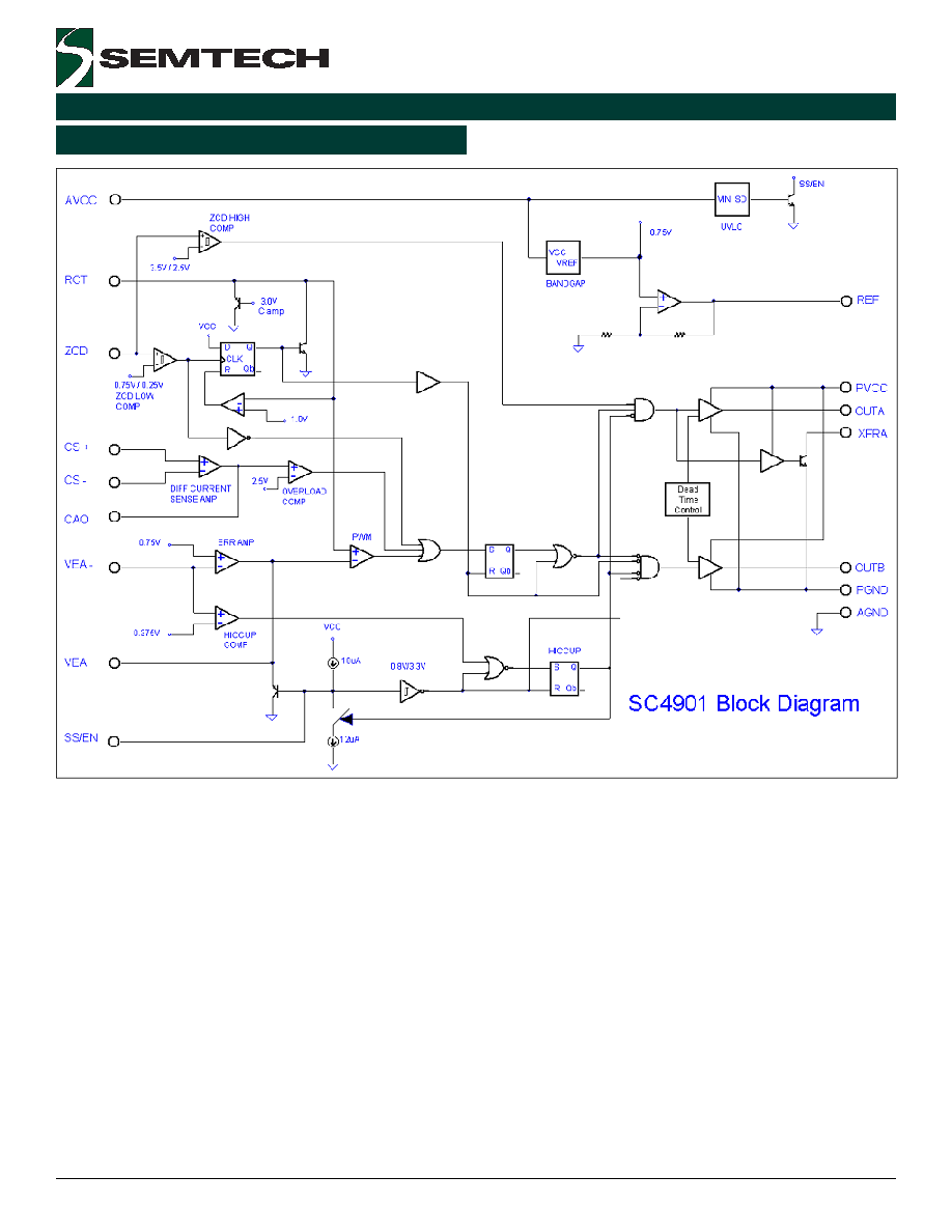
Pin Configurations
1
2
3
4
5
6
7
8
AGND
CS+
TOP VIEW
13
12
14
15
16
11
10
9
ZCD
CS-
RCT
CAO
VEA
SSEN
VEA-
AVCC
REF
OUTB
OUTA
XFRA
PVCC
PGND
Electrical Characteristics (Cont.)
Unless specified: T
A
=
25�C, V
CC
= 12V
r
e
t
e
m
a
r
a
P
s
n
o
i
t
i
d
n
o
C
t
s
e
T
n
i
M
p
y
T
x
a
M
t
i
n
U
s
r
e
v
i
r
D
t
u
p
t
u
O
A
T
U
O
e
g
a
tl
o
V
h
g
i
H
t
u
p
t
u
O
)
1
(
I
A
T
U
O
e
c
r
u
o
S
A
2
.
0
=
0
1
5
.
0
1
V
B
T
U
O
e
g
a
tl
o
V
h
g
i
H
t
u
p
t
u
O
)
1
(
I
B
T
U
O
e
c
r
u
o
S
A
1
.
0
=
0
1
5
.
0
1
V
A
T
U
O
-
e
g
a
tl
o
V
w
o
L
t
u
p
t
u
O
)
1
(
I
A
T
U
O
k
n
i
S
A
2
.
0
=
1
2
.
1
V
A
R
F
X
-
e
g
a
tl
o
V
w
o
L
t
u
p
t
u
O
)
1
(
I
A
R
F
X
k
n
i
S
A
2
.
0
=
1
2
.
1
V
B
T
U
O
-
e
g
a
tl
o
V
w
o
L
t
u
p
t
u
O
)
1
(
I
B
T
U
O
k
n
i
S
A
1
.
0
=
1
2
.
1
V
e
m
i
T
ll
a
F
d
n
a
e
s
i
R
C
A
T
U
O
F
p
0
0
0
2
=
0
3
S
n
C
B
T
U
O
F
p
0
0
0
1
=
0
3
S
n
g
n
i
s
i
R
B
T
U
O
o
t
g
n
il
l
a
F
A
T
U
O
T
A
C
�
5
8
o
t
C
�
0
4
-
=
5
8
0
1
1
5
3
1
S
n
Notes:
1) Only available in tape and reel packaging. A reel
contains 2500 devices.
2) Lead free product

5
2004 Semtech Corp.
www.semtech.com
SC4901
POWER MANAGEMENT
Pin Descriptions
#
n
i
P
e
m
a
N
n
i
P
n
o
i
t
c
n
u
F
n
i
P
1
+
S
C
.
r
e
if
il
p
m
a
t
n
e
r
r
u
c
l
a
it
n
e
r
e
f
fi
d
e
h
t
o
t
t
u
p
n
i
g
n
it
r
e
v
n
i
n
o
n
e
s
n
e
s
t
n
e
r
r
u
C
.
V
m
0
0
2
s
i
-
S
C
o
t
t
r
w
l
a
it
n
e
r
e
f
fi
d
m
u
m
i
x
a
M
2
-
S
C
.
r
e
if
il
p
m
a
t
n
e
r
r
u
c
l
a
it
n
e
r
e
f
fi
d
e
h
t
o
t
t
u
p
n
i
g
n
it
r
e
v
n
i
e
s
n
e
s
t
n
e
r
r
u
C
3
O
A
C
.
n
i
p
s
i
h
t
t
a
V
5
.
2
o
t
t
e
s
s
i
d
l
o
h
s
e
r
h
t
ti
m
il
t
n
e
r
r
u
C
.
r
e
if
il
p
m
a
t
n
e
r
r
u
c
l
a
it
n
e
r
e
f
fi
d
e
h
t
f
o
t
u
p
t
u
O
4
N
E
S
S
s
e
v
i
r
d
e
t
a
g
e
h
t
h
t
o
b
n
w
o
d
t
u
h
s
ll
i
w
V
5
6
.
0
w
o
l
e
b
n
i
p
s
i
h
t
g
n
i
k
a
T
.
n
i
p
e
l
b
a
n
E
d
n
a
t
r
a
t
S
t
f
o
S
5
C
C
V
A
.
V
8
1
o
t
p
u
s
i
g
n
it
a
r
x
a
M
.
e
g
a
tl
o
v
y
l
p
p
u
s
g
o
l
a
n
A
6
B
T
U
O
.
T
E
F
S
O
M
g
n
i
y
fi
t
c
e
r
e
d
i
s
w
o
l
e
h
t
r
o
f
e
v
i
r
d
e
t
a
G
7
A
R
F
X
.
ri
a
p
T
E
F
S
O
M
d
r
a
w
r
o
f
l
a
n
o
it
c
e
ri
d
i
b
e
h
t
f
o
r
e
v
i
r
d
e
t
a
g
e
h
t
r
o
f
n
o
it
c
e
n
n
o
c
r
e
m
r
o
f
s
n
a
r
T
.
A
T
U
O
o
t
d
e
s
i
n
o
r
h
c
n
y
s
l
a
n
i
m
r
e
t
r
o
t
c
e
ll
o
c
n
e
p
o
g
n
i
k
n
i
s
t
n
e
r
r
u
c
h
g
i
H
.
n
i
p
s
i
h
t
o
t
r
e
m
r
o
f
s
n
a
r
t
e
v
i
r
d
e
t
a
g
e
h
t
f
o
d
n
e
r
e
w
o
l
e
h
t
t
c
e
n
n
o
C
8
D
N
G
P
.
s
t
n
e
r
r
u
c
e
v
i
r
d
e
t
a
g
r
o
f
n
r
u
t
e
r
d
n
u
o
r
G
9
C
C
V
P
.
s
ti
u
c
ri
c
e
v
i
r
d
e
t
a
g
e
h
t
r
o
f
y
l
p
p
u
s
r
e
w
o
P
.
D
N
G
P
o
t
r
o
ti
c
a
p
a
c
c
i
m
a
r
e
C
F
u
1
a
d
n
a
c
it
y
l
o
r
t
c
e
l
e
F
u
0
1
f
o
m
u
m
i
n
i
m
a
h
ti
w
s
s
a
p
y
B
0
1
A
T
U
O
.
ri
a
p
T
E
F
S
O
M
d
r
a
w
r
o
f
l
a
n
o
it
c
e
ri
d
i
b
e
d
i
s
h
g
i
h
e
h
t
r
o
f
e
v
i
r
d
e
t
a
G
1
1
F
E
R
.
e
s
u
l
a
n
r
e
t
x
e
r
o
f
V
5
.
2
f
o
e
g
a
tl
o
v
t
u
o
e
c
n
e
r
e
f
e
R
.
n
i
p
e
h
t
m
o
r
f
n
w
a
r
d
e
b
n
a
c
A
m
5
o
t
p
U
2
1
-
A
E
V
V
5
7
.
0
s
i
l
e
v
e
l
e
c
n
e
r
e
f
e
R
.
t
u
p
n
i
g
n
it
r
e
v
n
i
r
e
if
il
p
m
a
r
o
r
r
e
o
t
k
c
a
b
d
e
e
f
e
s
n
e
s
e
g
a
tl
o
v
t
u
p
t
u
O
3
1
A
E
V
.
n
o
it
a
s
n
e
p
m
o
c
k
c
a
b
d
e
e
f
r
o
f
t
u
p
t
u
o
r
e
if
il
p
m
a
r
o
r
r
E
4
1
T
C
R
.
r
o
ti
c
a
p
a
c
d
n
a
r
o
t
s
i
s
e
r
g
n
i
m
it
e
h
t
r
o
f
n
i
p
n
o
it
c
e
n
n
o
C
5
1
D
C
Z
d
n
a
y
r
a
d
n
o
c
e
s
r
e
m
r
o
f
s
n
a
r
t
e
h
t
f
o
s
n
o
it
i
s
n
a
r
t
e
h
t
s
t
c
e
t
e
D
.
t
c
e
t
e
D
r
e
v
o
s
s
o
r
C
o
r
e
Z
.
s
t
n
e
n
o
p
m
o
c
T
C
R
y
b
p
u
t
e
s
p
m
a
r
e
h
t
s
e
s
i
n
o
r
h
c
n
y
s
e
d
i
s
w
o
l
e
h
t
n
o
D
N
G
A
o
t
d
e
p
m
a
l
c
y
ll
a
n
r
e
t
n
I
6
1
D
N
G
A
.
s
h
t
a
p
n
r
u
t
e
r
l
a
n
g
i
s
e
h
t
ll
a
r
o
f
d
n
u
o
r
G
g
o
l
a
n
A
6
2004 Semtech Corp.
www.semtech.com
SC4901
POWER MANAGEMENT
Block Diagram
7
2004 Semtech Corp.
www.semtech.com
SC4901
POWER MANAGEMENT
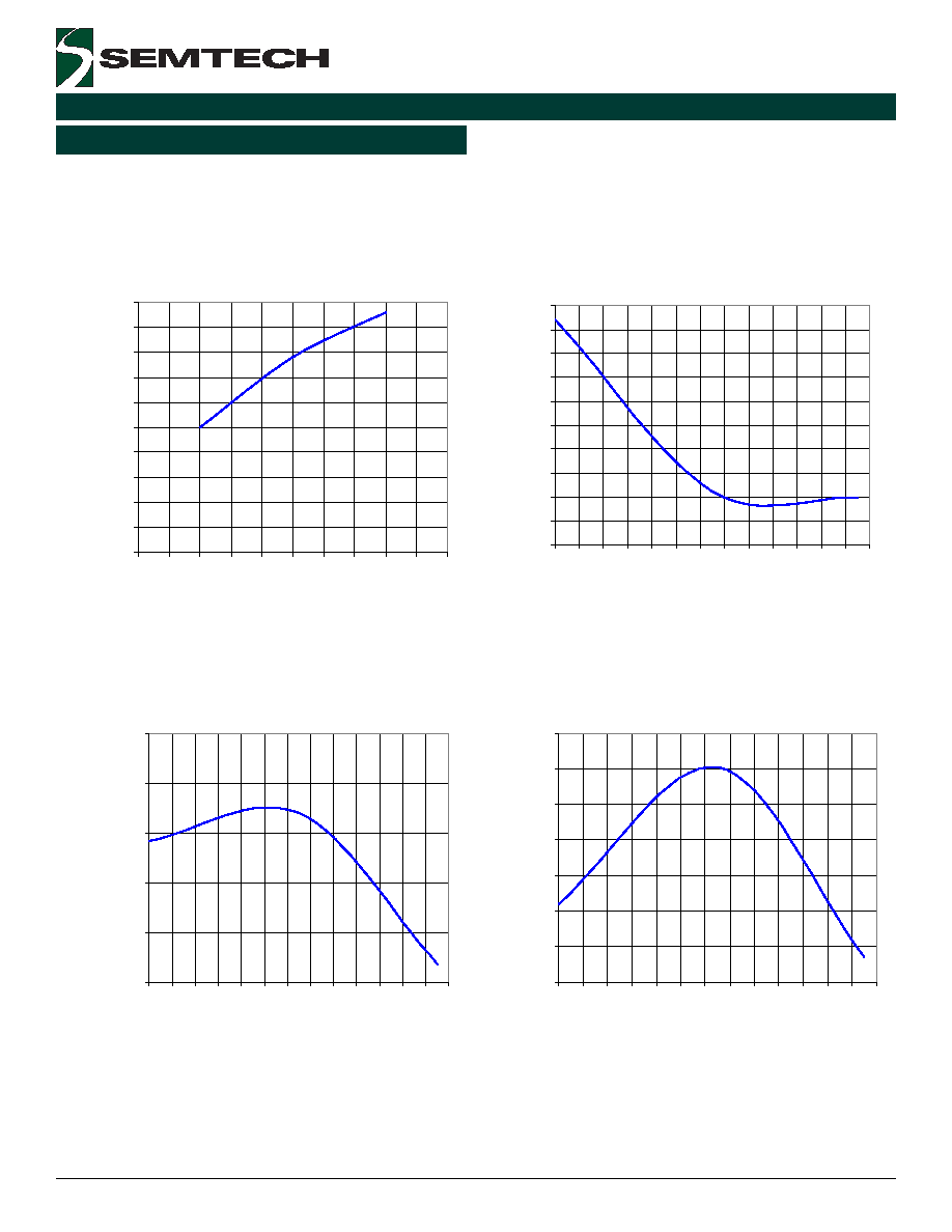
Charecteristic Curves
Current Amplifier Offset vs Temperature
-1.00
-0.50
0.00
0.50
1.00
1.50
2.00
2.50
3.00
3.50
4.00
-40 -30 -20 -10 0
10 20 30 40 50 60 70 80 90
Temperature (�C)
C
u
rre
n
t
A
m
p
O
ffs
e
t
(m
V
)
Internal Reference vs Temperature
0.7450
0.7470
0.7490
0.7510
0.7530
0.7550
-40 -30 -20 -10 0 10 20 30 40 50 60 70 80 90
Temperature (�C)
In
te
rn
a
l
R
e
f. (m
V
)
Quiescent Current vs AVCC
7.000
7.100
7.200
7.300
7.400
7.500
7.600
7.700
7.800
7.900
8.000
10
11
12
13
14
15
16
17
18
19
20
AVCC Volts
Q
u
i
e
s
cent
C
u
r
r
e
n
t
m
A
External Reference vs Temperature
2.49
2.50
2.50
2.50
2.50
2.50
2.51
2.51
-40 -30 -20 -10 0
10 20 30 40 50 60 70 80 90
Temperature (�C)
E
x
te
rn
a
l
R
e
fe
rn
c
e
8
2004 Semtech Corp.
www.semtech.com
SC4901
POWER MANAGEMENT
Applications Information
Introduction
The SC4901 is a voltage mode PWM controller for
implementing secondary side synchronous rectification
and simultaneous post regulation in forward convertors.
Multiple outputs can be derived off the same transformer
winding. Each output is independently regulated by
modulating the on time of the forward MOSFET pair which
acts as a bidirectional switch. An introduction to this unique
Combi Sync topology is presented later in this section.
The device takes the transformer secondary voltage as the
clock input and generates an internal ramp. The switching
frequency and maximum duty cycle are always determined
by the transformer waveform.
The output current is sensed as a low level differential input
signal. An amplified current signal is put out by the device
for further use in current share and hot swap applications.
Overload protection is achieved by peak current limiting
followed by hiccup mode under short circuit. A buffered
2.5V reference is also put out for system monitoring and
other purposes.
The controller implements the classical trailing edge
modulation and the outputs are complementary PWM
signals that drive the forward and rectifying MOSFETs. The
high side outputs can source up to + 2A peak current and
are configured for driving a pulse transformer with duty
ratios greater than 50%.
Undervoltage, Soft Start and Enable
The SC4901 has an operating range of 4.5V to 18V with
undervoltage lockout. Two conditions must be met before
the controller is operational. The input supply should be
above the undervoltage threshold of 4.5V and the SSEN
pin should be above 0.65V typical. If not, the device is
deactivated - the outputs are held active low, the SSEN
and the VEA pins are also held low. The controller is in
standby mode and draws only the quiescent current of 7
mA typical. Once the undervoltage threshold has been
exceeded and the SSEN pin is released, the soft start
capacitor at pin 5 is charged by a constant current of 10
�A. The VEA follows the SSEN voltage and the output
gradually ramps up. Once the SSEN pin charges to 3.3V,
the soft start cycle is complete and the device is fully
operational.
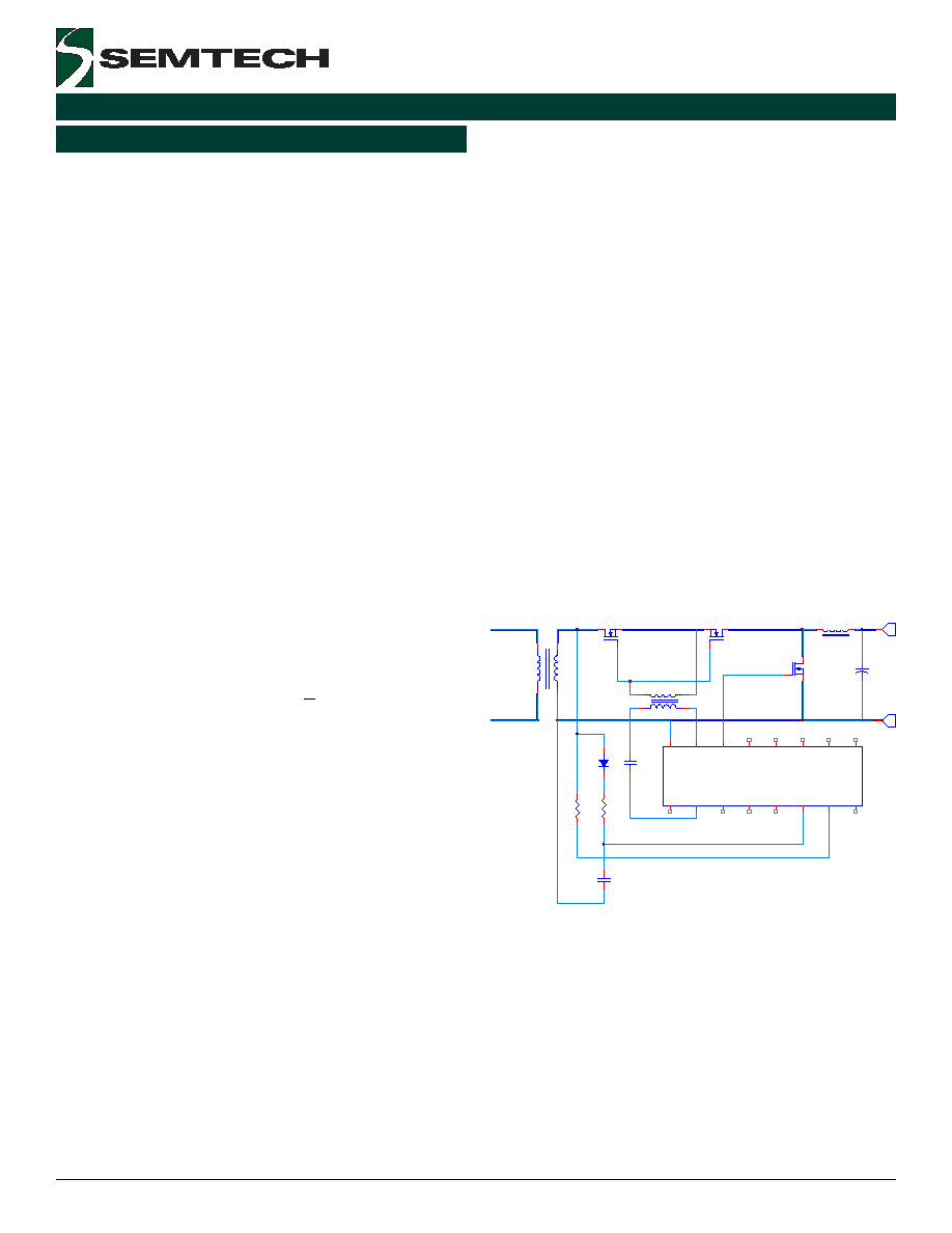
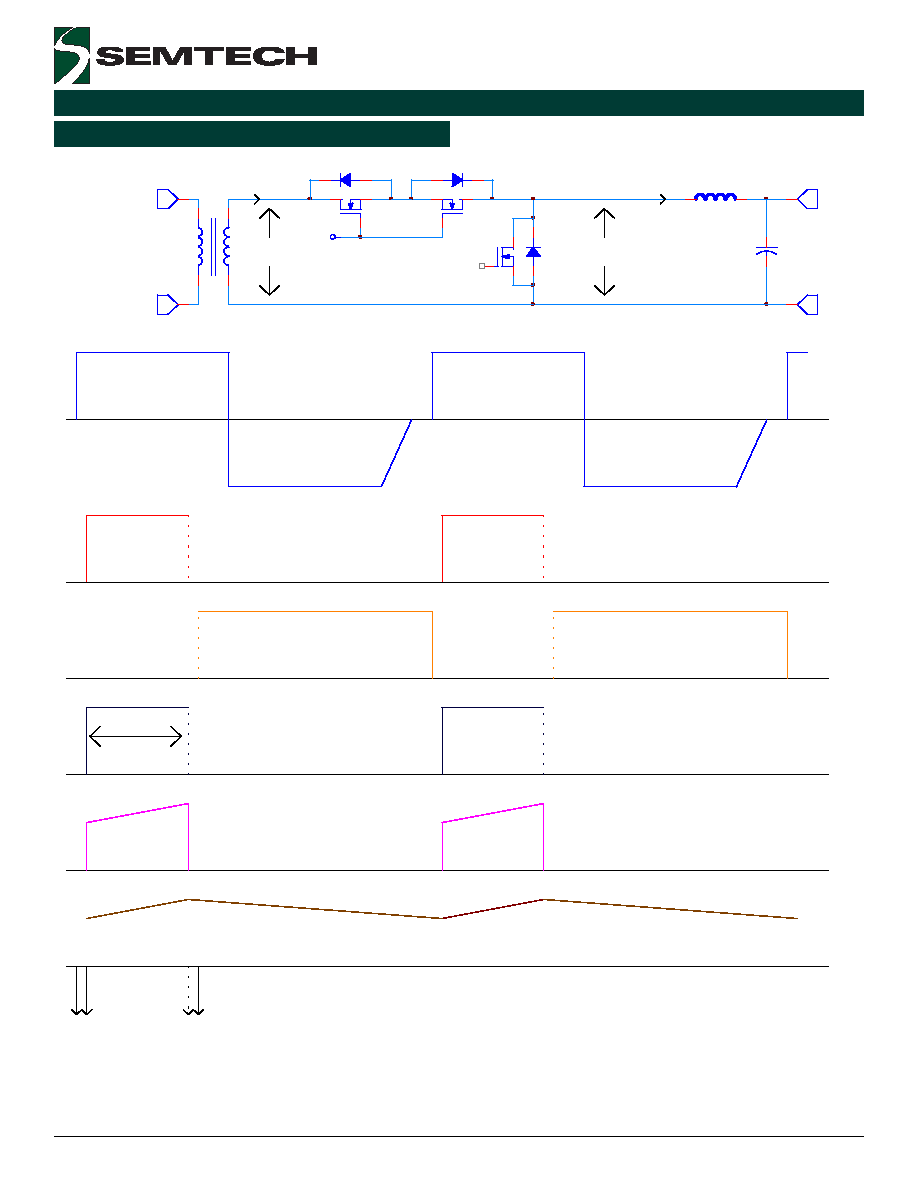
ZCD and RCT
Since the SC4901 is specifically designed for secondary
side control, the oscillator is always derived from the
transformer winding. Special care must be taken to ensure
that the transformer voltage, with all its variations in rise
time, shape, magnitude and duty ratio is translated into a
steady ramp on a cycle by cycle basis. SC4901 provides
two pins, ZCD and RCT, for this purpose.
The transformer voltage is sensed at the Zero Crossover
Detect or the ZCD pin. A limiting resistor, RZ in the Typical
Application Circuit, from the winding to ZCD pin is required
to limit the input current into the pin to 5 mA under all
conditions. The ZCD pin has two comparators with
hysteretic thresholds. One comparator has lower thresholds
of 0.75/0.25V and the other has 3.5V/2.5V. Together they
ensure proper turn on and turn off timings for the forward
and the rectifying FETs. There is also an internal clamp
which prevents the pin voltage from going below zero.
Ensure that the ZCD pin is not forced into any negative
voltage by external circuits.
Fig 1. Generating the Zero Crossover Detect (ZCD) and the
Timing Ramp (RCT) signals
The RCT pin has a timing capacitor CT connected to AGND
and a charging resistor RT connected to the source, which
is typically derived from the transformer voltage. Refer to
the Typical Applications Circuit on the first page. The RCT
pin is clamped to 3V peak internally and the ramp operates
between 1V and 3V. The high side forward pulse is
terminated whenever the RCT ramp hits the 3V peak.
QS
QF
QR
� �
T1
L1
C2
RZ
RT
��
T2
D1
U?
SC4901
ZC
D
15
CA
O
3
CS
-
2
CS
+
1
OU
T
B
6
SS
E
N
4
XF
R
A
7
PV
CC
9
PG
N
D
8
AVC
C
5
AG
N
D
16
OU
T
A
10
RE
F
11
VE
A-
12
VE
A
13
RC
T
14
SINGLE
ENDED
FORWARD
CONVERTOR
R TN
V O U T
C3
CT

9
2004 Semtech Corp.
www.semtech.com
SC4901
POWER MANAGEMENT
Applications Information (Cont.)
Ensure that the ramp reaches this peak only after the
negative transition of the transformer voltage, even under
the worst case conditions of high line and maximum
applicable duty ratio. Otherwise the available pulse width
for post regulation will be limited. On the other hand, the
timing capacitor should get charged fully to 3V prior to
positive transition of the transformer voltage. This will
ensure that the dead time between the rectifying and
forward gate drives is consistently maintained. Ideally the
ramp should be charged to its peak of 3V just after the
falling edge of the transformer secondary voltage so that
the voltage error amplifier output utilises the full range of
1V to 3V. This is shown in the idealised waveforms below.
Fig 2. Idealised ZCD and RCT waveforms
The idealised waveforms above are easier to implement if
the transformer has some form of constant volt-second
operation or control; the secondary voltage can be directly
used to charge the timing capacitor CT. If the transformer
operates in open loop with constant ON time, it is
recommended that the timing capacitor be charged from
a constant voltage. The maximum input current into the
RCT pin under clamped conditions should be limited to 2
mA.
Turn On Sequence
Prior to transformer voltage going positive, the ramp
capacitor is at its maximum of 3.0V. On the rising edge of
transformer secondary, 0.75V at the ZCD pin is detected
first and OUTB gate drive goes low which turns off the low
side rectifying FET QR (Fig. 1). Simultaneously a current
sink of 10 mA is activated to discharge the timing capacitor
CT to the lower threshold of 1V. This discharge time
provides the delay between turn off of rectifying FET and
turn on of the forward MOSFETs and is given by
2
.
0
�
= CT
DLon
where CT is the ramp capacitor value in pF and DLon is
the dead time in nS. The actual dead time is extended by
the propagation delays internal to the controller, which
should be taken into account while choosing CT. The
propagation delays are typically in the range of a few tens
of nanoseconds.
When the RCT pin goes down to 1V, the discharge is
stopped and the timing capacitor CT charges back up.
Meanwhile, on the rising edge of ZCD pin, a higher
threshold of 3.5V is detected. Once both these conditions
have been met, OUTA goes high, XFRA and the forward
FETs QS and QF are turned on. The CT capacitor is typically
charged from the transformer secondary voltage through
RT. Having chosen CT to meet dead time requirements, RT
is chosen so that the ramp voltage is just below 3.0V peak
at the end of the maximum ON time.
where
Vsec = Peak value of transformer secondary voltage
fsw = Switching frequency in kHz
D = Operating duty cycle at which Vsec is applied
If the primary side is PWM modulated in a feedback loop
or has a volt second clamp, the term Vsec x D is constant.
If it is free running with a fixed duty cycle, use the maximum
value of Vsec. The formula assumes that Vsec is much
larger than the ramp voltage of 3.0V. For lower secondary
voltages, use a smaller value of RT.
fsw
Const
D
V
RT
�
�
�
= sec
ZCD INPUT
XFR SEC
VOLTAGE
RCT RAMP
10
2004 Semtech Corp.
www.semtech.com
SC4901
POWER MANAGEMENT
REF Output and Error Amplifier
The reference level for output voltage feedback is 0.75V
bandgap. This is amplified, buffered and put out as a 2.5V
REF output. The REF voltage can be used for external
monitoring circuits or for regulating output voltages less
than 0.75V. The output of the error amplifier can swing
between 0.3V to 2.9V, just below the clamped peak of the
timing ramp. The REF pin should be bypassed to AGND
with a 0.1 uF ceramic capacitor. A maximum of 5 mA can
be drawn from the REF output.
Delays and Turn Off Sequence
The delay between turn off of the rectifying MOSFET QR to
the turn on of the forward MOSFETs QS and QF is
determined by the discharge of the ramp capacitor CT
through a 10 mA current. The other delay, between turn
off of the forward MOSFETs and turn on of the rectifying
MOSFET is fixed and typically 110 nS. This delay is valid
when the output is in regulation and the forward FETs are
turned off by the PWM comparator. During transients or if
the output loses regulation, QS and QF will be turned off
on the falling edge of the transformer voltage. First, the
high comparator detects the 2.5V threshold and pulls down
OUTA. This turns off the forward FETs. Further down, the
lower comparator detects the 0.25V threshold and turns
on OUTB. This ensures that the forward FET pair is off
before transformer voltage goes negative.
Current Sense and Current Limit
Current sensing is done as the input of an uncommitted
differential amplifier. The current limit threshold is 2.5V at
the CAO pin. This allows the user considerable flexibility to
design the current sensing circuit. A very low value sense
resistor which results in a current signal of a few tens of
millivolts or inductor drop sensing can be used for simple
protection and maximum efficiency. The current amplifier
gain has to be correspondingly higher. A larger current
sense signal with lower gain may be preferred for better
noise immunity and more precise current limit. Maximum
recommended differential input is 200 mV and minimum
differential gain for the current amplifier is 10, to ensure
proper operation. The CAO output is typically 2V at full load.
This signal can be brought out and used further for current
sharing applications. The current sense pins have a
maximum common mode range of AVCC - 2V.
Applications Information (Cont.)
When 2.5V limit is reached at CAO pin, the bidirectional
forward switch QS/QF is turned off for the rest of the cycle.
The rectifying FET is kept ON throughout to discharge the
high inductor current. As the overload level is increased,
the ON time continues to reduce and the output drops
gradually. The output is continuously monitored for
undervoltage and when it falls below 50% of the nominal
voltage, an abnormal condition is detected and both the
outputs are shut down. The soft start capacitor is
discharged by a 2 uA current sink down to 0.8V at which
point a soft start cycle is initiated to restart the convertor.
This effectively provides hiccup mode of protection under
short circuit.
Output Drivers
There are two complementary outputs designated A and
B. Output A and XFRA are the PWM drives that control the
bidirectional forward MOSFETs. The complementary output
for driving the ground referenced rectifying MOSFET QR is
designated as OUTB. This drive is capable of sourcing and
sinking +1A. OUTA is enabled when the transformer
voltage turns on and ZCD voltage exceeds 3.5V. It is turned
off on any one of the three conditions.
a) the ramp voltage on RCT exceeds the error amplifier
output at VEA or
b) ZCD detects that the transformer voltage is turning off
and gone below 2.5V or
c) overcurrent is detected at 2.5V on the CAO pin.
In all these cases OUTA and XFRA are turned off and, after
a fixed delay of 110 nS, the rectifier MOSFET is turned on.
Both OUTA and XFRA can sink or source + 2A peak current.
Fig 3. Driving a Pulse Transformer using XFRA and OUTA
U1
SC4901
ZC
D
15
CA
O
3
CS
-
2
CS
+
1
OU
T
B
6
SSE
N
4
XF
R
A
7
PV
C
C
9
PG
N
D
8
AVC
C
5
AG
N
D
16
OU
T
A
10
RE
F
11
VE
A-
12
VE
A
13
RC
T
14
QS
QF
QR
� �
T1
L1
C1
C5
C2
R3
R2
R1
R4
C3
��
T2
D1
D3
SINGLE
ENDED
FORW ARD
CON VERTOR
VOUT
OU
T
A
XFRA
PVCC
D2
C4

11
2004 Semtech Corp.
www.semtech.com
SC4901
POWER MANAGEMENT
Since OUTA has to drive a level shifted MOSFET gate, it
must be used with a pulse transformer. Another pin called
XFRA is provided to simplify the gate drive design with a
1:1 transformer. The XFRA is configured as a high current
open collector transistor and is turned on and off
synchronously with OUTA. If the maximum duty cycle
expected is less than 50%, the pulse transformer can be
connected directly between OUTA and XFRA. This ensures
that the gate is always driven with PVCC during both on
and off periods. A 1A Schottky or ultrafast rectifier should
be connected in reverse across the XFRA transistor. Refer
to D3 in Fig. 3) This is required to discharge the MOSFET
gate rapidly during turn off. In addition, a smaller signal
diode should be connected from XFRA to PVCC supply to
reset the driver transformer. This diode may be rated to
carry the magnetising current of the drive transformer.
Refer D2 in Fig 3).
If maximum duty ratio is more than 50% a ceramic cap C4
is added in series to the transformer primary as shown in
Fig 3). The capacitor carries a small voltage only when duty
ratio is more than 50%. Note that the common source of
the high side FETs presents a negative voltage to the return
pin of any high side drive circuit and therefore a
semiconductor driver is not recommended in this
application. The drive circuits are powered by a separate
supply and ground pair, designated as PVCC and PGND.
Adequate and independent noise bypassing of both AVCC
and PVCC to the corresponding grounds is strongly
recommended.
Reference Design and Typical Waveforms
The complete schematic of a secondary side channel
delivering 3.3V/10A is shown in Fig 4) Typical waveforms
are shown Figs 5) to Fig 8) These waveforms were taken
on a dual output convertor with 48V input and a
transformer turns ratio of 6:1. The two outputs were rated
at 3.3V/10A and 2.5V/10A. Of special interest are the
primary side waveforms shown in Fig 8) The zero current
turn on can be clearly seen. During turn off, the current
decreases as 2.5V forward FETs turn off first, followed by
3.3V output. The last small step at final turn off represents
the magnetising current in transformer primary.
Layout Guidelines
The Combi Sync topology and SC4901 are intended for
use in multi output convertors and demand careful
attention to good layout practices. The topology has an
inherent advantage in that all switching circuits naturally
operate at the same frequency set by the primary controller.
But the operating duty ratio is different for different outputs
and this may cause unexpected interferences. Make sure
that the currents in the RTN path are kept separate and
returned to a single node at the transformer end. High
current returns from one output should be isolated from
the signal current returns going into the AGND pins of other
outputs. A dedicated ground plane is strongly
recommended to improve noise immunity.
SC4901 requires a clean synchronising signal at the ZCD
pin to ensure proper operation. There are several sources
that may contribute to the noise at this pin. The traces
from the transformer terminals to the corresponding QS
drain and QR source pins must be kept to the absolute
minimum. When the FETs are turned ON or OFF, the current
in the transformer secondary winding is subjected to a rapid
rate of di/dt. Long traces that encompass wide areas have
higher parasitic lead inductances. The combination of a
rapid di/dt and large parasitic inductance is a dip or spike
in the transformer waveform which can confuse the ZCD
pin and lead to random transitions at the output. The series
resistor RZ shown in the Typical Application Circuit should
have a separate connection to the transformer secondary
terminal where the source waveform is relatively free of
distortions.
The primary side layout also requires special attention.
Excessive ringing or spikes on the primary side will be
reflected to the secondary and interfere with the controller
operation. It is important to physically separate the primary
and secondary circuits and use separate ground planes to
minimise interference.
The drive transformer for the forward FETs can contribute
significantly to the overall performance. For fast rise and
fall times and low switching losses, choose a driver with
low inductances. The traces from the transformer to OUTA
and XFRA pins must be kept short to minimise the overall
inductance in the drive path.
Applications Information (Cont.)
12
2004 Semtech Corp.
www.semtech.com
SC4901
POWER MANAGEMENT
Applications Information (Cont.)
Fig 4) Secondary side schematic
for a 3.3V/10A output.
13
2004 Semtech Corp.
www.semtech.com
SC4901
POWER MANAGEMENT
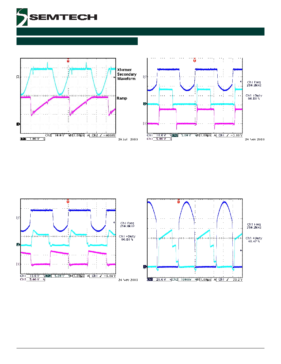
Applications Information (Cont.)
FIg 5) Transformer secondary voltage and ramp at RCT
pin
Fig 7) Transformer scondary voltage (top),
rectified PWM output for 2.5V (center)
and rectified PWM output for 3.3V (bottom)
Fig 6) Transformer scondary voltage (top),
OUTA gate drive for forward MOSFET pair (center)
and OUTB gate drive for the rectifying FET (bottom)
Fig 8) Primary MOSFET waveforms
Drain to Source Voltage (Blue) and
Current (green) .
14
2004 Semtech Corp.
www.semtech.com
SC4901
POWER MANAGEMENT
Combi-Sync Topology
Combi-Sync is a unique secondary side topology that
overcomes most of the problems associated with
synchronous rectification of isolated outputs. It also
incorporates synchronous post regulation, making it the
ideal solution for low voltage, high current outputs.
Independently regulated multiple outputs can be derived
from a common transformer winding. The output stage
replaces the conventional rectifiers and regulators with
three MOSFETs, two of which switch at zero voltage. The
topology inherently eliminates turn on shoot through
without complicated timing or look ahead circuits to
maximise efficiency. All secondary switching circuits are
naturally synchronised to primary which simplifies noise
suppression. There are no separate synchronising, current
sensing or gate driving signals crossing the isolation
boundary. In most cases, there will be no need for a
separate bias supply on the secondary side further
simplifying the system design.
The primary side in a Combi-Sync circuit is a typical single
ended forward convertor which may be regulated or free
running. An additional benefit of the Combi-Sync topology
is the zero current turn on and turn off for the primary
MOSFET as well. The free running mode is preferred when
there are multiple outputs without minimum load and cross
regulation constraints. Input voltage feedforward is
recommended to achieve volt-second clamp and minimise
core losses in the free running mode.
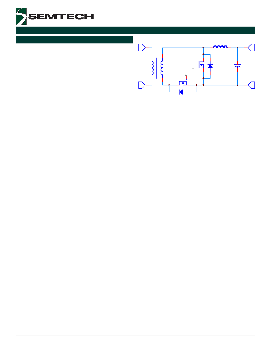
Background on Synchronous Rectification and Post
Regulation
The synchronous rectifier technology is widely used in non
isolated DC-DC convertors but its use has been limited in
isolated convertors because of various difficulties. An
example of synchronous rectification on the secondary side
of a forward convertor is shown in Fig 9. DF and DR are
the parasitic body diodes of their respective FETs. The
forward MOSFET QF is turned ON when the transformer
secondary voltage goes positive and the rectifying MOSFET
QR is turned ON when the transformer secondary is
negative. Two approaches have been used to drive the
MOSFETs. One is the self driven scheme where the
transformer secondary itself provides the gate voltage for
the appropriate FET. While the scheme is simple and has
a very low cost, it has several limitations.
Fig 9) Isolated Synchronous Rectification
One is that QR can conduct synchronously only while the
transformer is being reset. Thereafter there is no gate
voltage to drive it and the circuit must employ diode.
Secondly since the gate voltages, and the peak of
transformer secondary, must be with 4.5V to 20V under
all conditions, the scheme may fail at lower voltage and
wide input ranges.
An alternative is to use a control driven approach where a
synchronous controller provides the gate drive. This
provides the low loss FET conduction over the entire cycle
and is not limited by output or input ranges. However it is
not without its own problems. At the instant transformer
voltage turns positive the body diode of QF gets forward
biased. At the same time, QR would also be fully conducting
and the result is a shorted winding just when the primary
switch is trying to turn ON. To prevent catastrophe it is
necessary to turn QR OFF prior to transformer voltage going
positive. This requires an advanced signal from the primary
side crossing the isolation boundary. Attempts have been
made to avoid this by complex timing or look ahead circuits
on the secondary side itself and several patents have been
issued for them.
It should be understood that all these techniques for
isolated synchronous rectification have been restricted to
a single unregulated secondary output. . . . . The existing
circuits only rectify the output but do not synchronously
regulate it any further. Nor is it possible to generate multiple
outputs from the same winding. Post regulation of the
isolated outputs has been implemented so far using either
the saturable magnetic inductor or a power MOSFET in
series with the forward diode. The saturable magnetic
element is bulky and inefficient at high frequencies. The
circuit with series MOSFET is widely known and well
documented. Fig 10) shows a standard implementation.
Applications Information (Cont.)
QR
QF
DF
� �
DR
15
2004 Semtech Corp.
www.semtech.com
SC4901
POWER MANAGEMENT
Applications Information (Cont.)
The series FET QS is turned ON and OFF in a controlled
manner synchronously with the secondary waveform. The
width of the ON time pulse is varied to regulate the output.
Fig 10) Synchronous Post Regulation
Again it should be understood that all previous attempts
have used a non synchronously rectified secondary. . . . . That
is, the transformer secondary was rectified using power
diodes and the series MOSFET was added to synchronously
regulate it further.
The Combi Sync Technique
The Combi Sync, as the name indicates is a unique
secondary configuration that combines synchronous
rectification and post regulation on transformer isolated
multiple secondary voltages. The proposed implementation
as well as typical waveforms are shown in Fig 11) on the
next page. The highlights of its operation are as follows
a) Prior to the transformer voltage going positive, the
rectifying MOSFET QR is conducting. When the voltage goes
positive, QR is turned OFF.
b) After a delay, both QF and QS are turned ON. This delay
prevents both high and low side FETs conducting at the
same time and shorting the secondary winding.
c) The forward pair of QS and QF acts as a bidirectional
switch and can be turned off in a controlled manner
irrespective of the polarity of the transformer voltage. This
is the key to the topology. With SC4901 the forward pair is
turned off on any of the following conditions i) end of the
active PWM duration ii) peak current crosses the overload
limit or, iii) transformer secondary voltage begins to fall.
d) After the forward FETs QS and QF are turned OFF, the
rectifying FET QR is turned after a short delay. QR continues
to conduct until the beginning of the next cycle when
transformer secondary voltage goes positive again. By
modulating the ON time of the high side power MOSFETs
output regulation is achieved.
This arrangement of MOSFETs and their control provides
a highly efficient combination of synchronous rectification
and simultaneous control of isolated secondary voltages.
Trailing Edge Modulation
The Combi Sync topology offers the option of both leading
and trailing edge modulations to achieve synchronous post
regulation. With leading edge modulation, QS and QF are
turned on during the forward mode, with a PWM dictated
delay, but the turn off is synchronised to the falling edge
of the transformer voltage. This results in zero current turn
on for the primary switch but a hard turn off with full load.
On the other hand, in conventional secondary side post
regulation, the trailing edge modulation results in hard turn
on and zero current turn off for the primary switch. However,
the Combi Sync topology already has an inherent turn on
delay for the forward FETs on the secondary side. This
ensures zero current turn on for the primary switch,
irrespective of the modulation scheme used. It is therefore
advantageous to use trailing edge modulation which now
results in both zero current turn on and turn off for the
primary switch. If some form of ZVS is used in primary
control, all of the switching losses may be eliminated on
the primary side. Trailing edge modulation is the method
employed in SC4901.
Switching Waveforms
Theoretical switching waveforms of the Combi Sync
topology are shown on the next page. The first is the
transformer secondary voltage which acts as the reference.
Second and third are the gate drives for forward and
rectifying FETs respectively. Rectified and pulse width
modulated output that appears before the LC filter stage
is shown next. Notice that this rectified output rises after a
delay which is crucial to isolated synchronous rectification.
In the simple isolated synchronous rectifiers, there is no
QS, and QF begins to conduct (initially through its body
diode) at the same instant as the transformer voltage going
positive. Transformer secondary and inductor currents are
also shown. The delay T1-T0 is set by the capacitor CT and
the T3-T2 delay is fixed internally in SC4901
DS
QS
� �
T
C
OUTP UT
16
2004 Semtech Corp.
www.semtech.com
SC4901
POWER MANAGEMENT
OUT P UT
QF
DF
C
� �
T
DR
QS
DS
QR
L
SIN GLE EN DED
F OR W A R D
C ON V ER TOR
PR IM A R Y
GATE F
G AT E R
V re c
V s e c
Ind C urre nt
Se c C urre nt
V s e c
GA TE F
V re c
Ind ucto r C urre nt
Tra nsf o rm e r Se co nd a ry C urre n t
Tra nsf o rm e r Se c V o lta ge
Ga te Driv e f o r
F o rw a rd M OSF E TS QS, QF
RECTIF IED SECON DARY V OL TAGE
W ITH POST REGU L ATION
Ga te Driv e F o r QR
GA TE R
T 3
T 2
T 1
T 0
Pulse W id th M o d u la te d b y
Se c o nd a ry Sid e C o ntro lle r
-V E
+ V E
T2 : QS , QF are t urne d OF F .
This e dge is Pulse Widt h M odulat e d t o po st - re gulat e t he out put .
T1 : F o rward MOS F ETs QS and QF are swit ched ON
T1 - T0 : F o rward de lay t o pre ve nt short ing the se co ndary winding
T3 - T2 : Turn OF F delay t o prev ent sho ot thro ugh
T3 : QR is t urne d ON
T0 : Transfo rme r se co ndary volt age go es +ve , QR is t urne d OF F at t his instant .
Applications Information (Cont.)
FIg 11) Theoretical waveforms of Combi Sync topology
17
2004 Semtech Corp.
www.semtech.com
SC4901
POWER MANAGEMENT
OU T P UT 1
OU T P UT 2
OU T P UT N
QS1
DSN
QR1
DS1
C2
DS2
L1
QRN
QFN
QR2
DRN
C1
QF1
QF2
DR2
QSN
� �
DFN
QS2
DR1
DF1
LN
L2
DF2
CN
GATE DRV2
GATE DRV1
GATE DRV N
Applications Information (Cont.)
Features and Applications of the Combi Sync Circuit
with SC4901
The Combi Sync topology is quite versatile and has a
number of useful features
a) There is no connection between primary and secondary
sides. No synchronising signals, drive pulses, voltage or
current information needs to be exchanged across the
isolation boundary. The bias supply for the controller is
also generated on the secondary side, eliminating the
additional burden of a low power bias supply. SC4901 is
designed to operate over a range of 4.5V to 18V AVCC
supply which is the typical range for MOSFET gate drives.
b) For multiple secondary windings, each winding can have
its own set of synchronous MOSFETs and each set can be
controlled by an individual SC4901 to generate
independently regulated outputs. There is no cross
regulation or minimum load requirement, each output can
be turned ON or OFF independently of others. Placing the
controller on the secondary side also helps to optimise
the transient response.
c) It is possible to have multiple sets of synchronous FETs
attached to the same transformer secondary and control
them individually as shown in Fig 12. This way multiple
secondary outputs with a common ground can be regulated
off the same secondary winding.
d) All secondary switching is synchronised automatically
with the transformer waveform. There is only one switching
frequency in the convertor which simplifies EMI filter
design. Zero current switching of the primary FET further
reduces the switching noise generated on the primary side.
e) A number of options can be used to generate and control
the transformer secondary voltage.
i) The primary may be free running, that is without being
regulated by a feedback loop. It may further employ
constant volt second operation to reduce magnetic
stresses. In this mode the duty cycle is always at an
optimum value to maximise the efficiency.
ii) The primary may be regulated in a feedback loop by one
of the outputs; such regulation will typically employ voltage
mode or average current mode control. Note that peak
current mode control is not suitable with the trailing edge
modulation.
f) It is necessary to drive the forward FETs through a
transformer interface. The common source of the two
devices is a floating return and will swing to the peak
negative voltage appearing at the transformer secondary;
see the Vsec waveform in Fig 11). This negative swing
does not allow a semiconductor device to be used for
driving the forward FET pair. An additional pin called XFRA
is provided in SC4901 to simplify the design of driver
transformer interface, particularly with duty ratios of >50%.
XFRA is an open collector sink which turns on and off
simultaneously with OUTA.
g) The no load condition at the output needs special
consideration in this topology. Under light load, the inductor
current is negative as in any synchronous rectifier. When
the synchronous MOSFET QR is turned off, the current is
interrupted and tends to charge the drain source capacitor
of QR. The back to back connected forward FETs prevent
this current being returned to the source. The resulting
overshoot on QR can be clamped by connecting a zener
and diode combination across the inductor as shown in
Fig 4). The zener clamp conducts only during the dead
time and also provides a small benefit of reducing the
voltage across the forward FETs during turn on. The detailed
application schematic in Fig 4) shows diode D1 and zener
D2 connected across the output inductor L1 to reduce the
no load spike.
Fig 12) Generating Multiple Outputs from the same
secondary winding using Combi Sync Topology
18
2004 Semtech Corp.
www.semtech.com
SC4901
POWER MANAGEMENT
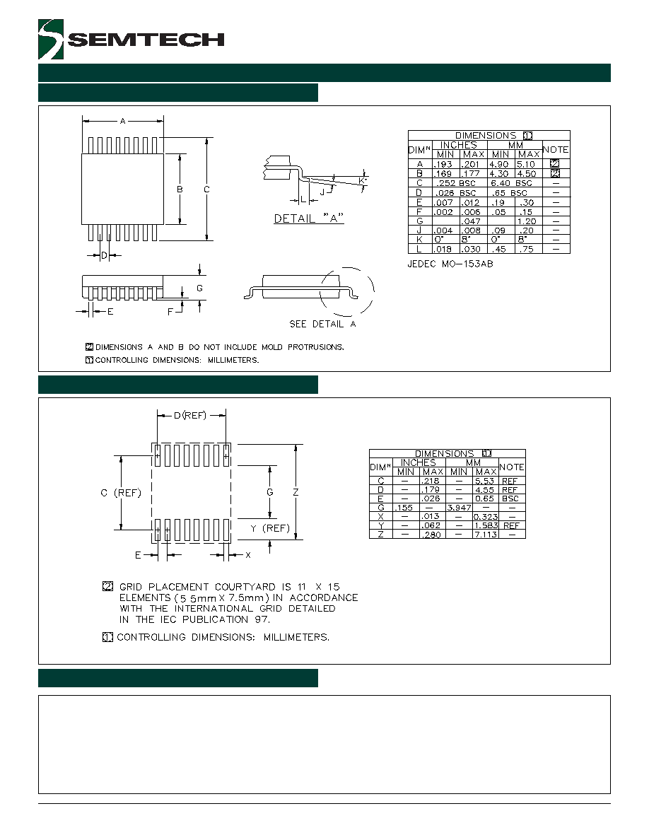
Outline Drawing - TSSOP-16
Semtech Corporation
Power Management Products Division
200 Flynn Road, Camarillo, CA 93012
Phone: (805)498-2111 FAX (805)498-3804
Contact Information
Land Pattern - TSSOP-16
.