1
www.semtech.com
SC4910A/B
High Performance Secondary Side
Controller with Synchronous Rectifier
POWER MANAGEMENT
Revision: May 11, 2005
Description
Features
Applications
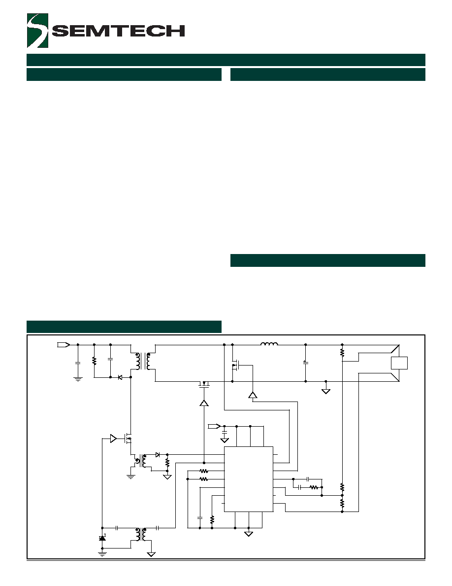
Typical Application Circuit
Synchronous rectification with adaptive control
Programmable secondary side delay
Programmable switching frequency
Programmable max. duty cycle
Remote voltage sense capability
Close-loop soft start with active low shutdown
0.75V precision reference for low output applications
Oscillator sychronization
Undervoltage Lockout
Operation to 1MHz
Current-mode or voltage-mode operation
Single stage power conversion with multiphase link
capability (with SC4201)
Monotonic start-up with pre-biased output
Active current sharing capability
20 pin TSSOP package
The SC4910A/B is an integrated, full featured, second-
ary side controller designed for use in single ended and
isolated switch mode power supplies with synchronous
rectification where efficiency and fast transient response
are of primary concern. The SC4910A/B has outputs for
both primary FET and secondary synchronous rectifica-
tion. The primary drive output is designed to drive a small
and low cost pulse transformer to isolate the primary
FET driver. The secondary control makes it much easier
to monitor and control the system load with tight control
loops and implement load current sharing and synchro-
nous rectification.
The SC4910A/B features synchronous rectification, multi-
phase link capability, programmable secondary side
delay, programmable switching frequency and program-
mable maximum duty cycle. It is designed for either
current mode or voltage mode operation.
The SC4910A has a typical turn-on threshold of 9V and
the SC4910B has a threshold of 4.5V.
+12V
C4
LOAD
C6
T3
R3
C5
C1
M1
SC1301
M2
R8
C10
R4
R7
T2
C2
R2
R6
L1
D2
SC4910
18
17
11
12
6
4
8
7
20
19
3
1
15
2
5
10
FB
COMP
OUTB
ISHARE
PHASE
CS
OUTA
PGND
RT1
RT2
SS
-SENSE
DELAY
SYNC/EN
VREF
PVCC
M3
SC1301
D3
C8
+Vin
R1
C9
SC1301
R9
C3
D1
R5
T1
16
13
14
PVCC
AVCC
9
PGND
AGND
Telecom isolated DC to DC converters
Isolated VRMS
Networking power supplies
Industrial power supplies
Distributed power architectures
High density power modules
2
2005 Semtech Corp.
www.semtech.com
SC4910A/B
POWER MANAGEMENT
Absolute Maximum Ratings
Electrical Characteristics
r
e
t
e
m
a
r
a
P
s
n
o
i
t
i
d
n
o
C
t
s
e
T
n
i
M
p
y
T
x
a
M
t
i
n
U
y
l
p
p
u
S
r
e
w
o
P
t
n
e
r
r
u
C
g
n
it
a
r
e
p
O
w
o
L
=
N
E
/
C
N
Y
S
0
1
5
1
A
m
t
u
o
k
c
o
L
e
g
a
t
l
o
v
r
e
d
n
U
d
l
o
h
s
e
r
h
T
t
r
a
t
S
A
0
1
9
4
C
S
7
.
8
0
.
9
3
.
9
V
B
0
1
9
4
C
S
5
3
.
4
0
5
.
4
5
7
.
4
V
s
i
s
e
r
e
t
s
y
H
O
L
V
U
A
0
1
9
4
C
S
0
0
4
0
5
5
0
0
7
V
m
B
0
1
9
4
C
S
0
0
2
0
0
3
5
7
3
V
m
e
c
n
e
r
e
f
e
R
F
E
R
V
e
g
a
tl
o
V
t
u
p
t
u
O
A
0
1
9
4
C
S
5
7
.
4
0
.
5
5
2
.
5
V
B
0
1
9
4
C
S
7
9
.
2
0
3
.
3
3
6
.
3
V
n
o
it
a
l
u
g
e
R
e
n
i
L
V
5
1
<
c
c
V
<
V
3
.
9
5
1
0
3
V
m
n
o
it
a
l
u
g
e
R
d
a
o
L
I
<
A
m
0
F
E
R
A
m
5
<
2
0
1
V
m
t
r
a
t
S
t
f
o
S
t
u
p
t
u
O
S
S
5
7
.
0
V
y
c
a
r
u
c
c
A
e
g
a
tl
o
V
T
A
T
=
J
C
�
5
2
=
1
-
1
+
%
5
.
1
-
5
.
1
+
n
o
it
a
l
u
g
e
R
e
n
i
L
V
5
1
<
c
c
V
<
V
3
.
9
5
-
0
5
+
V
m
e
c
n
a
d
e
p
m
I
)
2
(
K
7
r
e
t
e
m
a
r
a
P
l
o
b
m
y
S
m
u
m
i
x
a
M
s
t
i
n
U
e
g
a
tl
o
V
y
l
p
p
u
S
c
c
V
8
1
V
e
g
a
tl
o
V
t
u
p
t
u
O
c
c
V
V
e
s
a
h
P
c
c
V
V
E
R
A
H
S
I
,
N
E
/
C
N
Y
S
,
P
M
O
C
,
B
F
7
o
t
3
.
0
-
V
k
n
i
S
r
o
e
c
r
u
o
S
t
n
e
r
r
u
C
B
T
U
O
&
A
T
U
O
0
5
1
A
m
e
g
n
a
R
e
r
u
t
a
r
e
p
m
e
T
n
o
it
c
n
u
J
T
J
0
5
1
+
o
t
0
4
-
C
�
e
g
n
a
R
e
r
u
t
a
r
e
p
m
e
T
e
g
a
r
o
t
S
T
G
T
S
0
5
1
+
o
t
0
6
-
C
�
.
c
e
S
0
1
)
g
n
ir
e
d
l
o
S
(
e
r
u
t
a
r
e
p
m
e
T
d
a
e
L
T
D
A
E
L
0
6
2
C
�
Unless specified: T
A
=
T
J
= -40�C to 125�C , V
CC
= 12V, R
T1
= R
T2
= 50K, R
DELAY
= 50K, C
SS
= 0.1�F.
Exceeding the specifications below may result in permanent damage to the device, or device malfunction. Operation outside of the parameters specified
in the Electrical Characteristics section is not implied. Exposure to Absolute Maximum rated conditions for extended periods of time may affect device
reliability.
4
2005 Semtech Corp.
www.semtech.com
SC4910A/B
POWER MANAGEMENT
r
e
t
e
m
a
r
a
P
s
n
o
i
t
i
d
n
o
C
t
s
e
T
n
i
M
p
y
T
x
a
M
t
i
n
U
B
T
U
O
d
n
a
A
T
U
O
w
o
L
t
u
p
t
u
O
I
T
U
P
T
U
O
A
m
0
0
1
=
1
3
.
1
V
h
g
i
H
t
u
p
t
u
O
I
T
U
P
T
U
O
A
m
0
0
1
=
5
7
.
9
0
1
V
e
m
i
T
e
s
i
R
)
2
(
C
T
U
O
F
p
0
0
1
=
0
2
S
n
e
m
i
T
ll
a
F
)
2
(
C
T
U
O
F
p
0
0
1
=
0
2
S
n
y
a
l
e
D
g
n
i
s
i
R
A
T
U
O
o
t
g
n
il
l
a
F
B
T
U
O
)
2
(
R
Y
A
L
E
D
K
0
5
=
0
7
S
n
g
n
i
s
i
R
B
T
U
O
o
t
g
n
il
l
a
F
A
T
U
O
)
2
(
V
5
.
1
>
E
S
A
H
P
0
2
2
S
n
V
5
.
1
<
E
S
A
H
P
0
3
r
e
i
f
il
p
m
A
r
o
r
r
E
e
r
a
h
S
t
n
e
r
r
u
C
e
c
n
a
t
c
u
d
n
o
c
s
n
a
r
T
)
1
(
8
1
.
0
S
m
t
n
e
r
r
u
C
k
n
i
S
r
o
e
c
r
u
o
S
t
u
p
t
u
O
)
1
(
0
1
A
�
Electrical Characteristics (Cont.)
Notes:
(1) Guaranteed by design.
(2) Guaranteed by characterization.
(3) This device is ESD sensitive. Use of standard ESD handling requirements are required.
Unless specified: T
A
=
T
J
= -40�C to 125�C , V
CC
= 12V, R
T1
= R
T2
= 50K, R
DELAY
= 50K, C
SS
= 0.1�F.
5
2005 Semtech Corp.
www.semtech.com
SC4910A/B
POWER MANAGEMENT
r
e
b
m
u
N
t
r
a
P
e
g
a
k
c
a
P
T
R
T
S
T
I
A
0
1
9
4
C
S
)
2
(
0
2
-
P
O
S
S
T
)
1
(
T
R
T
S
T
I
B
0
1
9
4
C
S
)
2
(
Notes:
(1) Only available in tape and reel packaging. A reel
contains 2500 devices.
(2) Lead free product. This product is fully WEEE and
RoHS compliant.
Pin Configurations
Ordering Information
1
2
3
4
5
6
7
8
RT1
-SENSE
TOP VIEW
(20 Pin TSSOP)
13
14
15
16
RT2
SYNC/EN
FB
SS
COMP
CS
ISHARE
VREF
DELAY
PHASE
AVCC
AGND
PVCC
PGND
9
10
12
PVCC
PGND
OUTB
OUTA
11
18
17
19
20
Marking Information
Part Number (Example: 1471)
yyww = Date Code (Example: 0012)
xxxxx = Semtech Lot No. (Example: P94A01)
Part Number (Example: 1471)
yyww = Date Code (Example: 0012)
xxxxx = Semtech Lot No. (Example: P94A01)