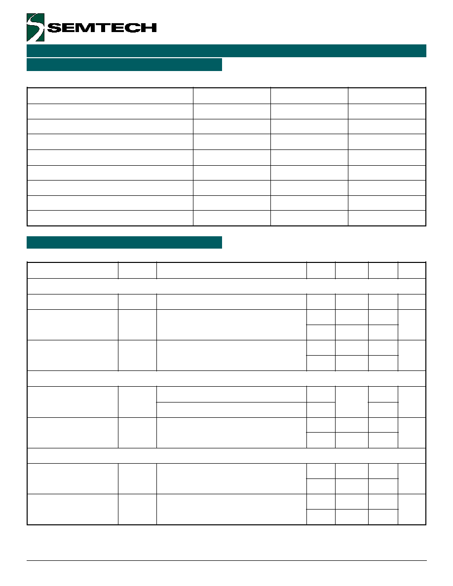
ChipFind - документация

Электронный компонент: SC553

Скачать:  PDF   ZIP
SC553 data sheet
background image
POWER MANAGEMENT
1
www.semtech.com
SC553
150mA Ultra Low Dropout
Regulator with Adjustable Output
.eatures
Revision 4, April 2002
Description
The SC553 is a low dropout linear regulator that
operates from a +2.25V to +6.5V input range and
delivers up to 150mA. A PMOS pass transistor allows
the low 75A supply current to remain independent of
load, making these devices ideal for battery operated
portable equipment such as cellular phones, cordless
phones and personal digital assistants.
The SC553 has an adjust pin (ADJ) enabling the user to
set the output voltage anywhere from 1.25V to 6V. .or a
low noise version, see SC1453 and for an error flag see
SC1457. Other features include low powered shutdown,
short circuit protection, thermal shutdown protection and
reverse battery protection. The SC553 comes in the tiny
5 lead SOT-23 package.
K
Battery Powered Systems
K
Cellular Telephones
K
Cordless Telephones
K
Personal Digital Assistants
K
Portable Instrumentation
K
Modems
K
PCMCIA cards
K
5205 compatible pinout
K
2% output accuracy guaranteed over line, load and
temperature
K
Guaranteed 150 mA output current
K
Very small external components - designed to work
with ceramic capacitors
K
Output adjustable from 1.25V to 6V
K
Very low supply current
K
Thermal overload protection
K
Reverse battery protection
K
Low power shutdown
K
.ull industrial temperature range
K
Surface mount packaging (5 pin SOT-23)
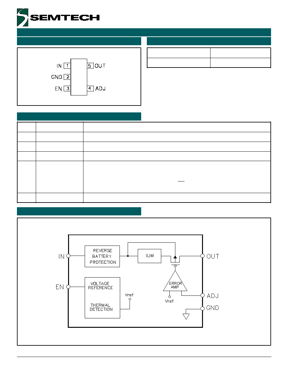
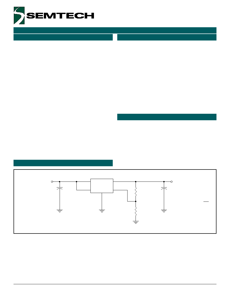
U1
SC553
1
2
3
4
5
IN
G N D
E N
ADJ
O U T
R2
C1
1uF
R1
VIN
C2
1uF
V O U T
Applications
Typical Application Circuit
+
=
2
R
1
R
1
250
.
1
V
OUT
background image
2
2002 Semtech Corp.
www.semtech.com
POWER MANAGEMENT
SC553
Absolute Maximum Ratings
r
e
t
e
m
a
r
a
P
l
o
b
m
y
S
m
u
m
i
x
a
M
s
t
i
n
U
e
g
a
t
l
o
V
y
l
p
p
u
S
t
u
p
n
I
V
N
I
7
+
o
t
6
.
0
-
V
e
g
a
t
l
o
V
e
l
b
a
n
E
V
N
E
V
o
t
6
.
0
-
N
I
V
t
n
e
i
b
m
A
o
t
n
o
i
t
c
n
u
J
e
c
n
a
t
s
i
s
e
R
l
a
m
r
e
h
T
A
J
6
5
2
W
/
C
e
s
a
C
o
t
n
o
i
t
c
n
u
J
e
c
n
a
t
s
i
s
e
R
l
a
m
r
e
h
T
C
J
1
8
W
/
C
e
g
n
a
R
e
r
u
t
a
r
e
p
m
e
T
t
n
e
i
b
m
A
g
n
i
t
a
r
e
p
O
T
A
5
8
+
o
t
0
4
-
C
e
g
n
a
R
e
r
u
t
a
r
e
p
m
e
T
n
o
i
t
c
n
u
J
g
n
i
t
a
r
e
p
O
T
J
5
2
1
+
o
t
0
4
-
C
e
g
n
a
R
e
r
u
t
a
r
e
p
m
e
T
e
g
a
r
o
t
S
T
G
T
S
0
5
1
o
t
5
6
-
C
.
c
e
S
0
1
)
g
n
i
r
e
d
l
o
S
(
e
r
u
t
a
r
e
p
m
e
T
d
a
e
L
T
D
A
E
L
0
0
3
C
Unless specified: V
IN
= 2.25V, V
EN
= V
IN
, I
OUT
= 100A, C
IN
= C
OUT
= 1F, T
A
= 25C. Values in bold apply over full operating ambient temperature range.
r
e
t
e
m
a
r
a
P
l
o
b
m
y
S
s
n
o
i
t
i
d
n
o
C
n
i
M
p
y
T
x
a
M
s
t
i
n
U
N
I
e
g
n
a
R
e
g
a
t
l
o
V
y
l
p
p
u
S
V
N
I
5
2
.
2
0
5
.
6
V
t
n
e
r
r
u
C
y
l
p
p
u
S
I
Q
I
T
U
O
V
5
2
.
2
,
A
m
0
5
1
o
t
A
m
0
=
V
N
I
V
5
.
6
5
7
0
3
1
A
0
6
1
t
n
e
r
r
u
C
y
l
p
p
u
S
e
t
a
t
S
-
f
f
O
I
)
F
F
O
(
Q
V
N
I
V
,
V
5
.
6
=
N
E
V
0
=
1
.
0
0
.
1
A
5
.
1
J
D
A
e
g
a
t
l
o
V
n
i
P
t
s
u
j
d
A
)
1
(
V
J
D
A
I
T
U
O
A
m
1
=
%
5
.
1
-
0
5
2
.
1
%
5
.
1
+
V
A
m
0
I
T
U
O
V
5
2
.
2
,
A
m
0
5
1
V
N
I
V
5
.
5
%
0
.
2
-
%
0
.
2
+
t
n
e
r
r
u
C
t
u
p
n
I
n
i
P
t
s
u
j
d
A
)
2
(
I
J
D
A
V
J
D
A
V
3
.
1
=
5
1
0
.
0
0
0
5
.
2
A
n
0
0
0
.
5
T
U
O
n
o
i
t
a
l
u
g
e
R
e
n
i
L
)
1
(
G
E
R
)
E
N
I
L
(
V
N
I
I
,
V
5
.
5
o
t
V
5
2
.
2
=
T
U
O
V
,
A
m
1
=
J
D
A
V
=
T
U
O
5
.
1
0
1
V
m
2
1
n
o
i
t
a
l
u
g
e
R
d
a
o
L
)
1
(
G
E
R
)
D
A
O
L
(
I
T
U
O
,
A
m
0
5
1
o
t
A
m
1
.
0
=
1
-
0
1
-
V
m
V
N
I
V
,
V
5
2
.
2
=
J
D
A
V
=
T
U
O
0
2
-
Electrical Characteristics
Exceeding the specifications below may result in permanent damage to the device, or device malfunction. Operation outside of the parameters specified
in the Electrical Characteristics section is not implied.
background image
3
2002 Semtech Corp.
www.semtech.com
POWER MANAGEMENT
SC553
Unless specified: V
IN
= 2.25V, V
EN
= V
IN
, I
OUT
= 100A, C
IN
= C
OUT
= 1F, T
A
= 25C. Values in bold apply over full operating ambient temperature range.
r
e
t
e
m
a
r
a
P
l
o
b
m
y
S
s
n
o
i
t
i
d
n
o
C
n
i
M
p
y
T
x
a
M
s
t
i
n
U
)
.
t
n
o
C
(
T
U
O
t
i
m
i
L
t
n
e
r
r
u
C
I
M
I
L
0
0
4
A
m
e
g
a
t
l
o
V
t
u
o
p
o
r
D
)
3
(
)
1
(
V
D
I
T
U
O
A
m
1
=
1
V
m
I
T
U
O
A
m
0
5
=
0
5
5
6
V
m
5
7
I
T
U
O
A
m
0
0
1
=
0
0
1
5
2
1
V
m
5
5
1
I
T
U
O
A
m
0
5
1
=
0
5
1
0
9
1
V
m
0
3
2
N
E
d
l
o
h
s
e
r
h
T
t
u
p
n
I
e
l
b
a
n
E
V
H
I
V
5
2
.
2
V
N
I
V
5
.
6
6
.
1
V
V
L
I
V
5
2
.
2
V
N
I
V
5
.
6
4
.
0
t
n
e
r
r
u
C
s
a
i
B
t
u
p
n
I
e
l
b
a
n
E
)
2
(
I
N
E
V
0
V
N
E
V
N
I
5
.
0
-
0
5
.
0
+
A
n
o
i
t
c
e
t
o
r
P
e
r
u
t
a
r
e
p
m
e
T
r
e
v
O
l
e
v
e
L
p
i
r
T
h
g
i
H
T
I
H
0
5
1
C
s
i
s
e
r
e
t
s
y
H
T
T
S
Y
H
5
1
C
Notes:
(1) Low duty cycle pulse testing with Kelvin connections required.
(2) Guaranteed by design.
(3) V
OUT
= 3.3V. Defined as the input to output differential at which the output voltage drops 100mV below the value
measured at a differential of 1V. Not measurable on outputs set below 2.25V due to minimum V
IN
constraints. See
Typical Characteristics for typical dropout voltage at other output voltage settings.
Electrical Characteristics (Cont.)
background image
4
2002 Semtech Corp.
www.semtech.com
POWER MANAGEMENT
SC553
Note:
(1) Only available in tape and reel packaging. A reel
contains 3000 devices.
r
e
b
m
u
N
t
r
a
P
e
g
a
k
c
a
P
R
T
K
S
I
3
5
5
C
S
)
1
(
5
-
3
2
-
T
O
S
Top View
SOT-23-5L
Pin Configuration
Ordering Information
Block Diagram
#
n
i
P
e
m
a
N
n
i
P
n
o
i
t
c
n
u
F
n
i
P
1
N
I
.
n
i
p
t
u
p
n
I
2
D
N
G
.
d
e
d
e
e
n
f
i
g
n
i
k
n
i
s
t
a
e
h
r
o
f
d
e
s
u
e
b
n
a
C
.
n
i
p
d
n
u
o
r
G
3
N
E
.
d
e
s
u
g
n
i
e
b
t
o
n
f
i
N
I
o
t
t
c
e
n
n
o
C
.
n
i
p
e
l
b
a
n
e
h
g
i
h
e
v
i
t
c
A
4
J
D
A
t
i
u
c
r
i
C
n
o
i
t
a
c
il
p
p
A
l
a
c
i
p
y
T
e
e
s
(
r
e
d
i
v
i
d
r
o
t
s
i
s
e
r
l
a
n
r
e
t
x
e
n
a
o
t
n
i
p
s
i
h
t
g
n
i
t
c
e
n
n
o
C
.
n
i
p
t
s
u
j
d
A
V
s
t
e
s
)
1
e
g
a
p
n
o
T
U
O
:
o
t
5
T
U
O
.
A
m
0
5
1
o
t
p
u
g
n
i
c
r
u
o
s
,
t
u
p
t
u
o
r
o
t
a
l
u
g
e
R
Pin Descriptions
+
=
2
R
1
R
1
250
.
1
V
OUT
background image
5
2002 Semtech Corp.
www.semtech.com
POWER MANAGEMENT
SC553
yyww
Top Mark
Bottom Mark
yyww = Datecode (Example: 0108)
553
Marking Information
Applications Information
Theory Of Operation
The SC553 is intended for applications where very low
dropout voltage, low supply current and low output noise
are critical. It provides a very simple, low cost solution
that uses very little pcb real estate. Only two external
capacitors are required for operation.
The SC553 contains a bandgap reference trimmed for
optimal temperature coefficient which is fed into the
inverting input of an error amplifier. The output voltage
of the regulator is divided down externally using a
resistor divider and compared to the bandgap voltage
via the adjust pin (ADJ). The error amplifier drives the
gate of a low R
DS(ON)
P-channel MOS.ET pass device to
maintain V
OUT
such that V
ADJ
= V
RE.
.
An active high enable pin (EN) allows the regulator to be
shut down. Pulling this pin low causes the device to
enter a very low power shutdown mode, where it will draw
typically 0.1A from the input supply.
The regulator has its own current limit circuitry to
ensure that the output current will not damage the
device during output short, overload or start-up. The
current limit is guaranteed to be greater than 400mA to
allow fast charging of the output capacitor and high
initial currents for DSP initialization.
The SC553 includes thermal shutdown circuitry to turn
off the device if T
J
exceeds 150C (typical), with the
device remaining off until T
J
drops by 15C (typical).
Reverse battery protection circuitry ensures that the
device cannot be damaged if the input supply is
accidentally reversed, limiting the reverse current to less
than 1.5mA.
Component Selection - General
Output capacitor - Semtech recommends a minimum
capacitance of 1. at the output with an equivalent
series resistance (ESR) of < 1
over temperature. While
the SC553 has been designed to be used with ceramic
capacitors, it does not have to be used with ceramic
capacitors, allowing the designer a choice. Increasing the
bulk capacitance will further reduce output noise and
improve the overall transient response.
Input capacitor - Semtech recommends the use of a
1. ceramic capacitor at the input. This allows for the
device being some distance from any bulk capacitance
on the rail. Additionally, input droop due to load transients
is reduced, improving overall load transient response.
External voltage selection resistors - the use of 1%
resistors, and designing for a current flow
10A is
recommended to ensure a well regulated output (thus
R2
125k
). The output voltage (referring to .igure 1
below) will be:
+
=
2
R
1
R
1
250
.
1
V
OUT
U1
SC553
1
2
3
4
5
IN
G N D
E N
ADJ
O U T
R2
C1
1uF
R1
VIN
C2
1uF
V O U T
.igure 1