/home/web/doc/html/semtech/196258
www.semtech.com
POWER MANAGEMENT
SC605
Charge Pump
Flash LED Driver
December , 2005
Description
Features
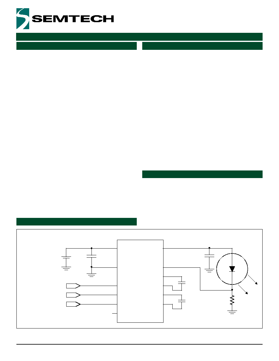
Typical Application Circuit
Features
Typical Application Circuit
Applications
The SC605 is a high-current charge pump designed spe-
cifically for use with white LEDs used in camera flash ap-
plications. Only two small bucket capacitors are required
to develop the output drive, providing a low EMI solution
compared to inductive boost regulators.
The SC605 has two modes of operation: Flash mode and
Spotlight mode. In Flash mode, the SC605 is capable of
delivering 500mA of regulated current for a duration of
500ms or up to 700mA for a reduced duration. In Spotlight
mode the SC605 can output 20%, 30%, or 40% of the Flash
mode current and remain enabled continuously.
An external resistor is connected in series with the LED to
set the current. In Flash mode, this resistor can dissipate
up to 0.75mW, reducing the power dissipation require-
ment of the SC605. The Flash input (FLASH) overrides
the control inputs (CTRL0 and CTRL1) to ensure the Flash
function has the highest priority.
The thermally efficient MLPD-12 package and ceramic
bypass and bucket capacitors help make the SC605 a
high output current driver that requires a minimal amount
of PCB area.
Two selectable modes - Flash and Spotlight
Up to 700mA output - Flash mode
Up to 280mA output - Spotlight mode
500mA output over specified temperature and volt-
age ranges - Flash mode
Spotlight mode selectable to 20%, 30%
and 40% of Flash current
3.0V to 5.25V input range
Flash control pin for synchronization to
a camera module or graphics controller
Short circuit, over-voltage and
over-temperature protection
Soft-start functionality
Three control inputs for maximum versatility
Shutdown current < 2A
Micro-lead package MLPD-12, 3mm x 3mm
VBAT
0�F
�F
white LED
CTRL
CTRL0
FLASH
0.5W
SC605
VIN
1
FLASH
6
CTRL0
8
CTRL1
9
NC
5
VOUT
11
ISET
7
C1+
10
C1-
4
C2+
12
C2-
2
�F
�F
GND
3
Mobile Camera Phones
Digital Cameras
PDAs with Built-in Cameras
2
2005 Semtech Corp.
www.semtech.com
POWER MANAGEMENT
SC605
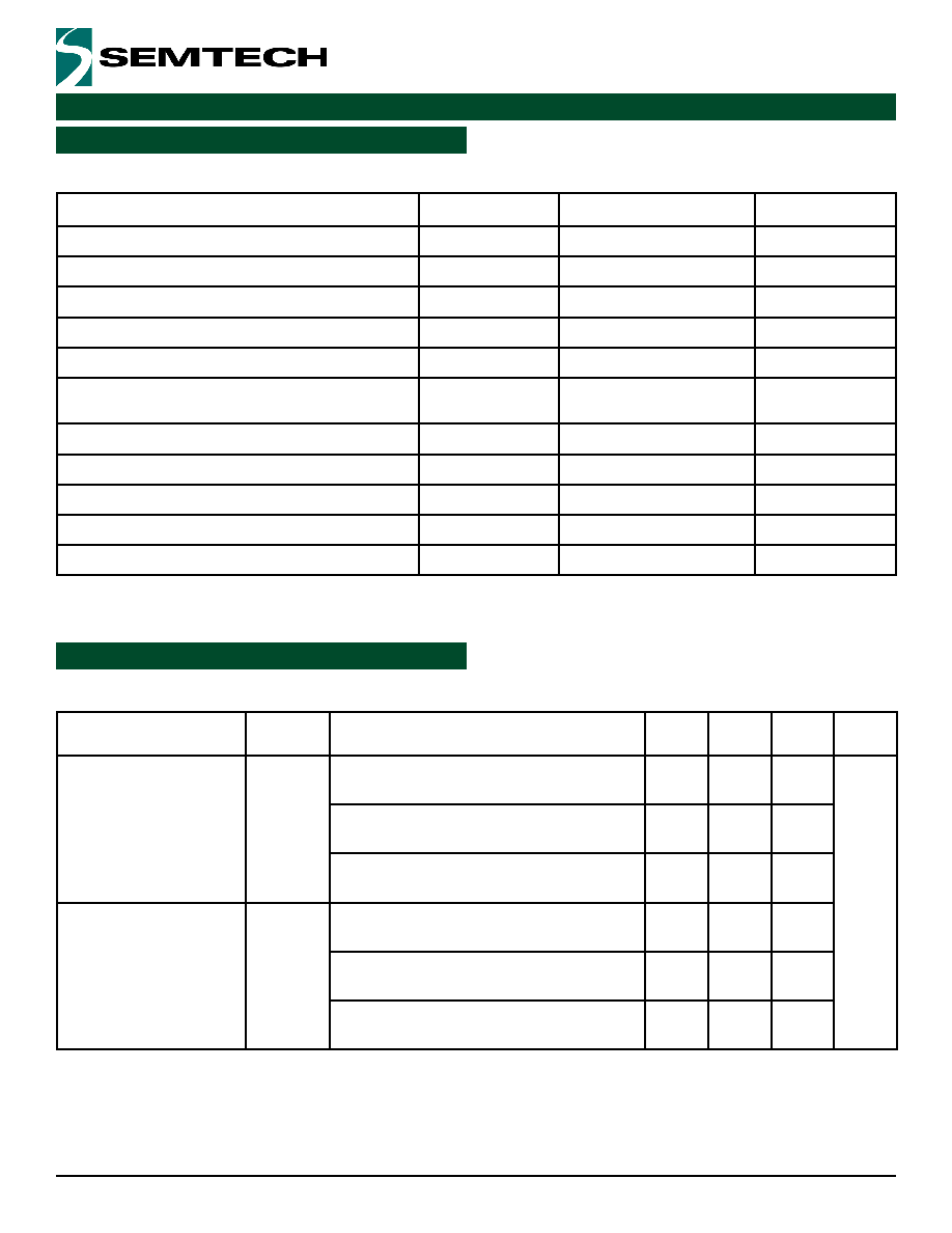
Absolute Maximum Ratings
Electrical Characteristics
Absolute Maximum Ratings
Exceeding the specifications below may result in permanent damage to the device or device malfunction. Operation outside the parameters specified in the
Electrical Characteristics section is not implied. Exposure to Absolute Maximum rated conditions for extended periods of time may affect device reliability.
Parameter
Symbol
Maximum
Units
Supply Voltage
V
IN
-0.3 to 6.5
V
Output Voltage
V
OUT
-0.3 to 6.5
V
Pin Voltage - FLASH, CTRL0, CTRL1, ISET, C1-, C2-
-0.3 to V
IN
+ 0.3
V
Pin Voltage - C1+, C2+
-0.3 to V
OUT
+ 0.3
V
V
OUT
Short Circuit Duration
SC
Indefinite
Thermal Resistance, Junction to Ambient
(JESD51 Standard Method)
(1)
JA
40
�C/W
Operating Ambient Temperature Range
T
A
-40 to +85
�C
Junction Temperature Range
T
JC
-40 to +150
�C
Storage Temperature Range
T
STG
-65 to +150
�C
IR Reflow Temperature
T
LEAD
260
�C
ESD Protection Level
(2)
V
ESD
2
kV
Notes:
1) Calculated from package in still air, mounted to 3" x 4.5", 4 layer FR4 PCB with thermal vias under the exposed pad per JESD51 standards.
2) Tested according to JEDEC standard JESD22-A114-B
Unless otherwise specified: T
A
= 25�C for TYP, -40�C to +60�C for MIN and MAX; C
IN
= 0�F, C
BUCKET
= C
OUT
= 1.0�F (ESR < 0.1);
V
IN
= 3.0V to 5.25V; V
OUT
= 2.8V to 4.25V; R
ISET
= 0.5 0.1%.
Parameter
Symbol
Conditions
Min
Typ
Max
Units
Flash Mode -
Output Current
I
OUT
FLASH high, R
ISET
= 0.357W,
3.7V < V
IN
< 4.2V, V
OUT
= 3.7V
(1)
700
mA
FLASH high, R
ISET
= 0.5W,
3.3V < V
IN
< 4.2V, 2.8V < V
OUT
< 4.25V
460
500
540
FLASH low, CTRL0 high, CTRL1 high, R
ISET
=
0.357W, 3.7V < V
IN
< 4.2V, V
OUT
= 3.4V
(1)
280
Spotlight Mode -
Output Current
I
OUT
FLASH low, CTRL0 high, CTRL1 high, R
ISET
=
0.5W, 3.0V < V
IN
< 4.5V, 2.8V < V
OUT
< 4.5V
170
200
230
FLASH low, CTRL0 low, CTRL1 high, R
ISET
=
0.5W, 3.0V < V
IN
< 4.5V, 2.8V < V
OUT
< 4.5V
120
150
180
(2)
FLASH low, CTRL0 high, CTRL1 low, R
ISET
=
0.5W, 3.0V < V
IN
< 4.5V, 2.8V < V
OUT
< 4.5V
70
100
130
(2)
3
2005 Semtech Corp.
www.semtech.com
POWER MANAGEMENT
SC605
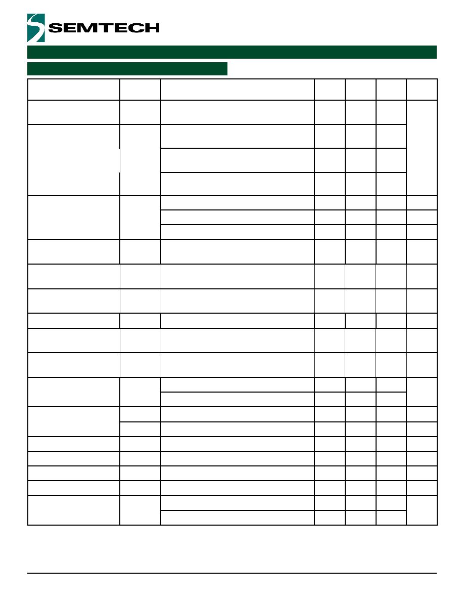
Electrical Characteristics (Cont.)
Parameter
Symbol
Conditions
Min
Typ
Max
Units
Flash Mode -
ISET Reference Voltage
V
ISET
FLASH high, R
ISET
= 0.5W,
3.3V < V
IN
< 4.2V, 2.8V < V
OUT
< 4.25V
230
250
270
mV
Spotlight Mode -
ISET Reference Voltage
V
ISET
FLASH low, CTRL0 high, CTRL1 high
3.0V < V
IN
< 4.5V, 2.8V < V
OUT
< 4.5V
85
100
115
FLASH low, CTRL0 low, CTRL1 high
3.0V < V
IN
< 4.5V, 2.8V < V
OUT
< 4.5V
60
75
90
(3)
FLASH low, CTRL0 high, CTRL1 low
3.0V < V
IN
< 4.5V, 2.8V < V
OUT
< 4.5V
35
50
65
(3)
Quiescent Current
I
Q
FLASH High
3.4
5
mA
FLASH low, CTRL0 and/or CTRL1 High
2.0
4.5
mA
FLASH low, CTRL0 low, CTRL1 Low
0.1
2
�A
Flash Mode
Pulse Duration
(4)
t
FLASH
3.3V < V
IN
< 4.2V
I
OUT
= 500mA
500
ms
Flash Mode
Start-Up Time
(4)
t
F-ST
from t = 0 when FLASH goes high to
I
OUT
= 90% of final value
1
ms
Spotlight Mode
Start-Up Time
(4)
t
S-ST
from t = 0 when CTRL0 and/or CTRL1 transi-
tion high to I
OUT
= 90% of final value
1
ms
Oscillator Frequency
f
OSC
Device Enabled
250
kHz
Oscillator Frequency
Accuracy
D
f
OSC
-15
15
%
Short-Circuit Ouput
Current Limit
I
SC
V
OUT
= 0V
465
mA
Input Current Limit
I
LIMIT
3.3V < V
IN
< 4.2V
1.0
2.1
A
V
IN
= 3.7V, V
OUT
= 3.7V, T
A
= 25�C
1.38
1.53
Over-Temperature
Protection
(4)
T
OT
150
�C
Hysteresis
10
�C
Logic Input High Threshold
V
IH
FLASH, CTRL0, CTRL1
1.5
V
Logic Input Low Threshold
V
IL
FLASH, CTRL0, CTRL1
0.4
V
Logic Input High Current
I
IH
FLASH, CTRL0, CTRL1
1
20
35
�A
Logic Input Low Current
I
IL
FLASH, CTRL0, CTRL1
0.1
2
�A
ISET Ripple Voltage
(4)
V
PP
Spotlight Mode, I
OUT
= 200mA
25
mV
Flash Mode, I
OUT
= 500mA
100
Notes:
(1) V
OUT
required by the typical LED at this current.
(2) Values do not overlap with the next higher spotlight mode for any single device. Expect Spotlight Modes to be separated by about 50mA.
(3) Values do not overlap with the next higher spotlight mode for any single device. Expect Spotlight Modes to be separated by about 25mV.
(4) Guaranteed by design - not tested in production.
2005 Semtech Corp.
www.semtech.com
POWER MANAGEMENT
SC605
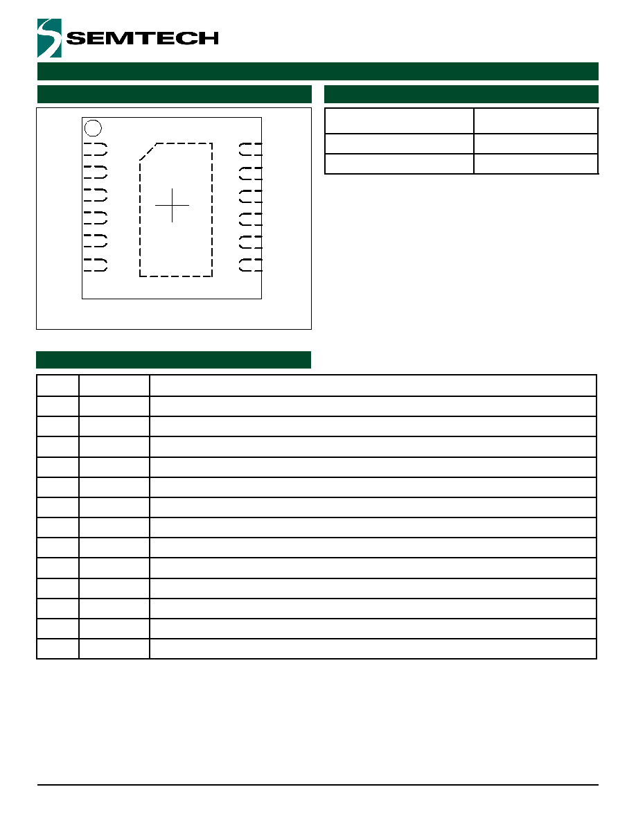
Pin Configuration
Pin Configuration
Ordering information
Pin Descriptions
DEVICE
PACKAGE
SC605MLTRT
(1)(2)
MLPD-12 3x3
SC605EVB
Evaluation Board
Notes:
(1) Available in Tape and Reel only. A reel contains 3000
devices.
(2) Available in lead-free package only. This product is fully
WEEE and RoHS compliant.
Pin
Pin Name
Pin Function (also see Suggested Layout guidelines on page 10)
1
VIN
Input voltage. Decouple with a 10�F or larger ceramic capacitor near pin 1.
2
C2-
Negative terminal of bucket capacitor 2 - use a 1�F ceramic capacitor.
3
GND
Ground - connect through multiple vias to the ground plane.
4
C1-
Negative terminal of bucket capacitor 1 - use a 1�F ceramic capacitor.
5
NC
Not connected - leave this pin floating.
6
FLASH
Flash mode enable pin - puts the device in active Flash mode when high.
7
ISET
Current-setting reference pin - connect to the LED cathode and the current setting resistor.
8
CTRL0
Control input bit 0 - used with CTRL1 to enable and set the output current in Spotlight mode (see Table 1).
9
CTRL1
Control input bit 1 - used with CTRL0 to enable and set the output current in Spotlight mode (see Table 1).
10
C1+
Positive terminal of bucket capacitor 1 - use a 1�F ceramic capacitor.
11
VOUT
Output pin - connect to LED anode. Decouple with a 1�F ceramic capacitor near pin 11.
12
C2+
Positive terminal of bucket capacitor 2 - use a 1�F ceramic capacitor.
T
Thermal Pad Pad for heat sinking purposes - not connected internally. Connect to ground plane using multiple vias.
TOP VIEW
2
3
5
MLPD- 12:3X312LEAD
T
6
2
0
8
7
VIN
C2-
GND
C-
NC
FLASH
ISET
CTRL0
CTRL
C+
VOUT
C2+
5
2005 Semtech Corp.
www.semtech.com
POWER MANAGEMENT
SC605
Applications Information
GeneralOperation
The SC605 is a powerful 2x charge pump designed to drive
a high-intensity white LED with a constant current (Spotlight
mode) or with a pulsed current of higher intensity (Flash
mode) used for camera flash.
In Flash mode the SC605 output can drive 500mA at 4.25V
into an LED for up to 500ms. The FLASH pin is used to
trigger Flash mode. In spotlight mode the SC605 regulates
the output current to the value selected by the CTRL0 and
CTRL1 inputs. Note that Flash mode has priority over
Spotlight mode, i.e., the FLASH pin triggers Flash mode
regardless of the state of the CTRL0 and CTRL1 pins.
Output current is regulated by attaching the ISET pin to the
cathode(s) of the LED package and a load sense resistor
(typically 0.5W). The ISET pin monitors the voltage at the
cathode and signals the charge pump to increase or de-
crease the output current until the ISET voltage reaches
the programmed setting. Programmed settings are shown
in Table 1:
CTRL1
CTRL0
FLASH
V
ISET
Mode
0
0
0
0mV
Disabled
0
1
0
50mV
Spotlight
1
0
0
75mV
Spotlight
1
1
0
100mV
Spotlight
x
x
1
250mV
Flash
Table1-ControlStateTable
The resistor value is chosen to set the current through the
LED based on this reference voltage. The resistor should
not be less than 0.35W due to the output current limitations
of the device. Note that the resistor sets both the Flash
mode current and the Spotlight mode current.
In Flash mode, I
OUT
= V
ISET
/ R
ISET
= 250mV / R
ISET
.
In Spotlight mode, I
OUT
= V
ISET
/ R
ISET
.
SpotlightMode
Spotlight mode is enabled by setting the CTRL0 and CTRL1
pins as shown in Table . When in Spotlight mode, the
SC605 can maintain a constant current indefinitely to drive
an LED or bank of LEDs. The ISET pin voltage is the refer-
ence V
ISET
and has three different settings - 50mV, 75mV,
and 100mV. These settings allow the designer the flexibility
to select the output level needed to suit the application.
FlashMode
Flash mode is enabled whenever the FLASH pin is pulled
high and remains active until the FLASH pin is released.
While in Flash mode the reference voltage on the ISET pin
is set to 250mV. During Flash mode the charge pump de-
velops enough output current to drive an LED with 500mA
for a duration up to 500ms. The duration of the pulse is
limited by the amount of power that can be dissipated in
the SC605 before it exceeds the maximum operating tem-
perature. Note that if an output current less than the rated
500mA is desired the duration of the pulse can increase
proportionally. However, great care should be taken to in-
sure the FLASH pin is not held high for an extended amount
of time so that overheating does not occur. Extending flash
mode beyond the 500ms pulse limit could adversely affect
the long-term reliability of the SC605. Flash duration must
be derated at higher currents, for example, 700mA derates
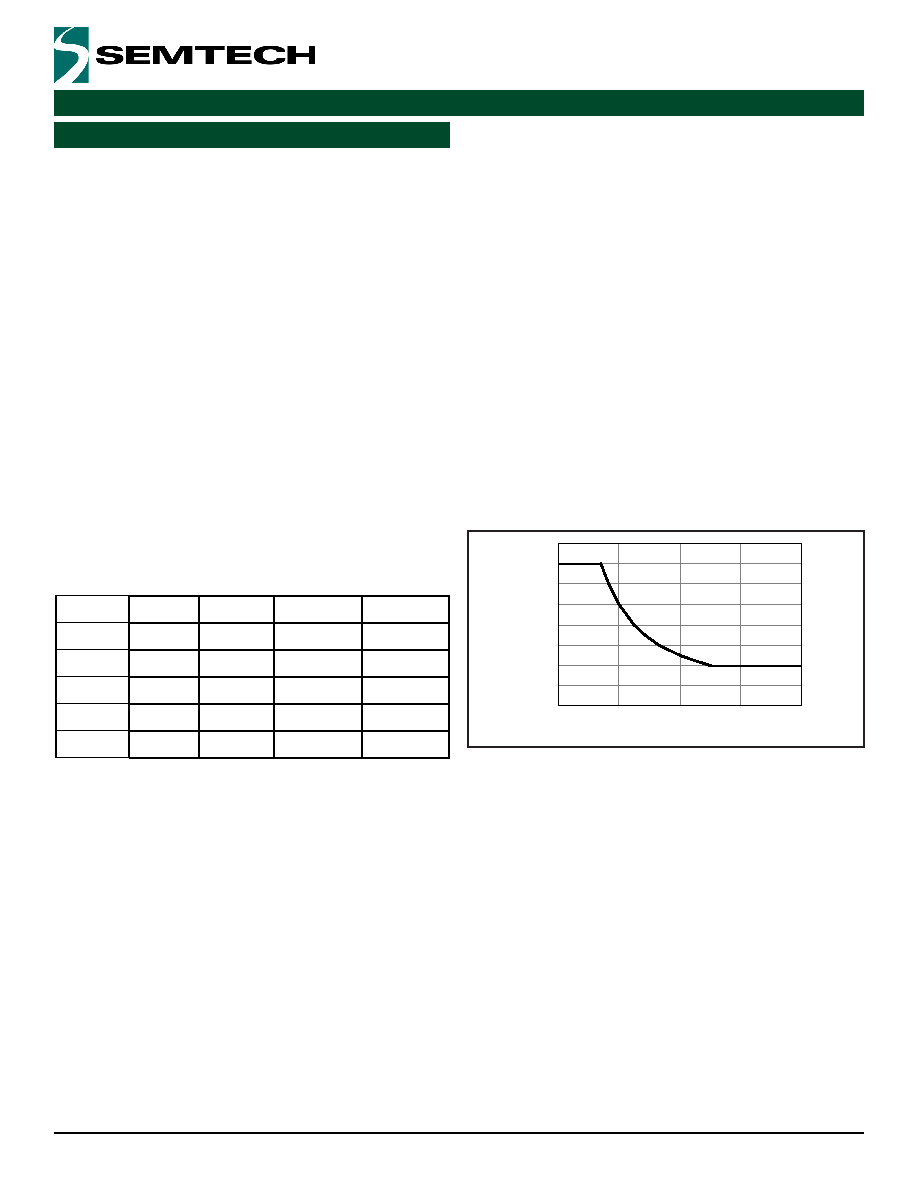
to a maximum of 350ms. The plot below shows maximum
Flash mode current for extended duration times.
MaximumFlashDuration
ProtectionCircuitry
The SC605 also provides protection circuitry that prevents
the device from operating in an unspecified state. These
include Input Over-Voltage Protection (IOVP), Output Over-
Voltage Protection (OVP), Over-Temperature Protection
(OTP), Over-Current Protection (OCP), and Short-Circuit
Current Protection (SCCP).
Input Over-Voltage Protection
Input over-voltage protection is included to prevent opera-
tion at high input voltages that could damage the device.
The IOVP circuit senses the input voltage and determines
when the supply exceeds 6V. When the voltage rises
above this threshold, the device is disabled until the input
voltage drops to a level within the specified input range.
Hysteresis is included in this circuit to avoid chattering
between states.
0
100
200
300
400
500
600
700
800
0
500
1000
1500
2000
Flash Duration [ms]
Flash Current [mA]