www.semtech.com
1
POWER MANAGEMENT
SC615
Charge Pump
Flash LED Driver
July 11, 2005
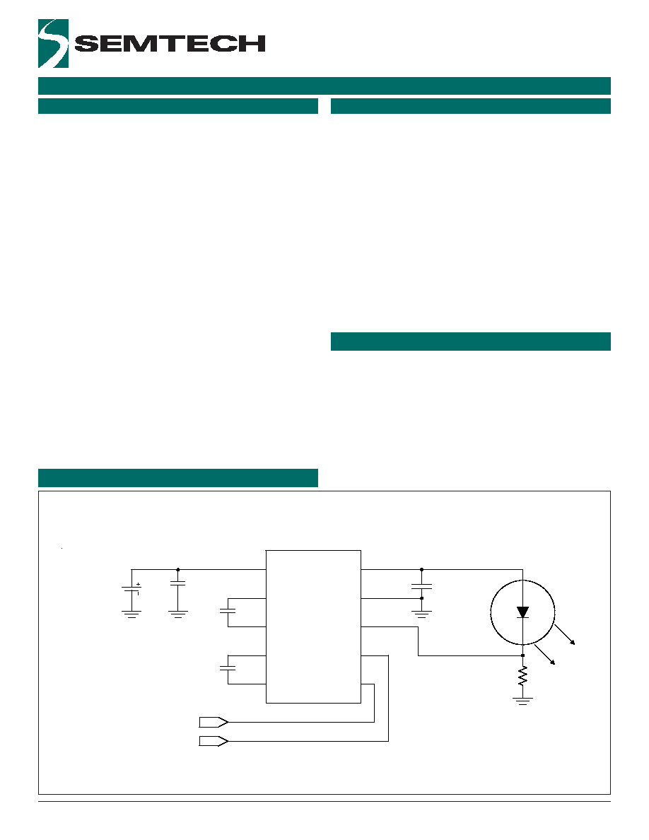
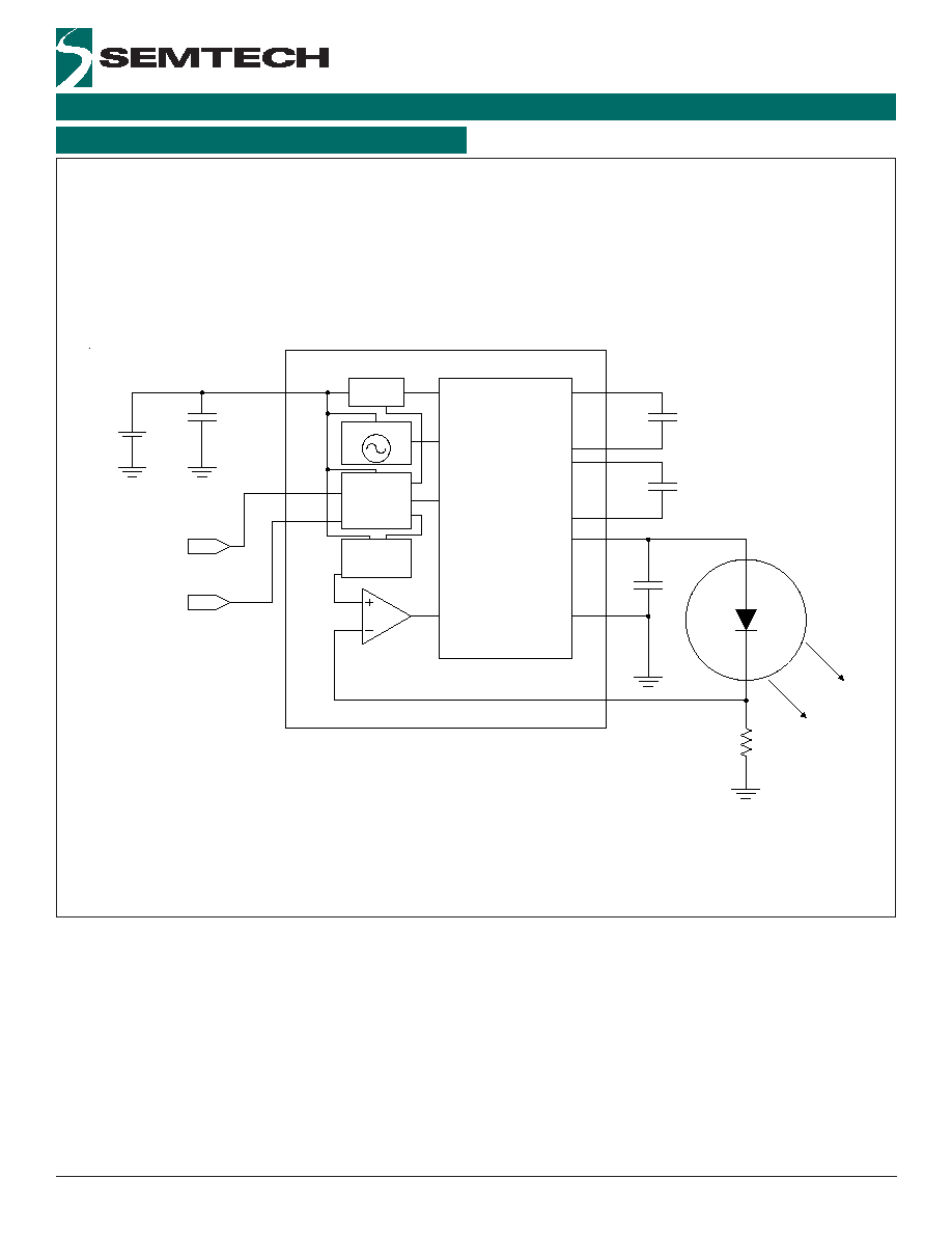
Application Circuit
Applications
Features
500mA Output Current - Flash Mode
3.0V to 5.25V Input Range
Two Selectable Modes - Flash and Spotlight
External Flash Control Pin for Synchronization to a
Camera Module or Graphics Controller
Spotlight Mode Current Setting - 100mA
Short Circuit, Over-Voltage, and Over-Temperature
Protection
Soft-Start Functionality
Two Control Inputs for Maximum Versatility
Shutdown Current < 2
µ
A
Micro Lead-frame Package MLPD-10, 3mm x 3mm
Mobile Camera Phones
Digital Cameras
PDAs with Built-in Cameras
Multi-LED Backlit LCDs
The SC615 is a high-current charge pump designed spe-
cifically for use with white LEDs used in camera flash
applications. Only two small bucket capacitors are re-
quired to develop the output drive, providing a low EMI
solution compared to inductive boost regulators.
The SC615 has two modes of operation: Flash mode
and Spotlight mode. The SC615 is capable of delivering
500mA of peak current for a duration of 500ms in Flash
mode. In Spotlight mode the SC615 outputs 100mA
and can remain enabled continuously.
A minimum 0.5
sense resistor is used to set the cur-
rent through the LED in both modes. This resistor dissi-
pates up to 0.125W, reducing the power dissipation re-
quirement of the SC615. The flash input (FLASH) over-
rides the control input (CTRL) to make sure the flash func-
tion is activated when called for.
The thermally efficient MLPD-10 package and ceramic
bypass and bucket capacitors help make the SC615 a
high output current driver that requires a minimal amount
of PCB area.
Description
3.0V to 5.25V
SC615
VIN
1
C2-
2
C2+
10
C1-
4
C1+
8
VOUT
9
FLASH
5
CTRL
7
GND
3
ISET
6
1
µF
1
µF
FLASH
CTRL
1
µF
white LED
0.5
10
µF
2
2005 Semtech Corp.
www.semtech.com
POWER MANAGEMENT
SC615
Notes:
1) Calculated from package in still air, mounted to 3"x 4.5", 4 layer FR4 PCB with thermal vias under the exposed pad per JESD51 standards.
2) Tested according to JEDEC standard JESD22-A114-B
r
e
t
e
m
a
r
a
P
l
o
b
m
y
S
m
u
m
i
x
a
M
s
t
i
n
U
e
g
a
tl
o
V
y
l
p
p
u
S
V
N
I
5
.
6
o
t
3
.
0
-
V
e
g
a
tl
o
V
t
u
p
t
u
O
V
T
U
O
5
.
6
o
t
3
.
0
-
V
-
2
C
,
-
1
C
,
T
E
S
I
,
L
R
T
C
,
H
S
A
L
F
-
e
g
a
tl
o
V
n
i
P
V
o
t
3
.
0
-
N
I
3
.
0
+
V
+
2
C
,
+
1
C
-
e
g
a
tl
o
V
n
i
P
V
o
t
3
.
0
-
T
U
O
3
.
0
+
V
V
T
U
O
n
o
it
a
r
u
D
ti
u
c
r
i
C
t
r
o
h
S
C
S
e
ti
n
if
e
d
n
I
t
n
e
i
b
m
A
o
t
n
o
it
c
n
u
J
,
e
c
n
a
t
s
i
s
e
R
l
a
m
r
e
h
T
)
d
o
h
t
e
M
d
r
a
d
n
a
t
S
1
5
D
S
E
J
(
)
1
(
A
J
9
4
W
/
C
∞
e
g
n
a
R
e
r
u
t
a
r
e
p
m
e
T
t
n
e
i
b
m
A
g
n
it
a
r
e
p
O
T
A
5
8
+
o
t
0
4
-
C
∞
e
g
n
a
R
e
r
u
t
a
r
e
p
m
e
T
n
o
it
c
n
u
J
T
C
J
0
5
1
+
o
t
0
4
-
C
∞
e
g
n
a
R
e
r
u
t
a
r
e
p
m
e
T
e
g
a
r
o
t
S
T
G
T
S
0
5
1
+
o
t
5
6
-
C
∞
e
r
u
t
a
r
e
p
m
e
T
w
o
lf
e
R
R
I
T
D
A
E
L
0
6
2
C
∞
l
e
v
e
L
n
o
it
c
e
t
o
r
P
D
S
E
)
2
(
V
D
S
E
2
V
k
Absolute Maximum Ratings
Electrical Characteristics
Unless otherwise specified: T
A
= 25∞C for TYP, -40∞C to +60∞C for MIN and MAX;
C
BUCKET
= C
OUT
= 1.0µF (ESR < 0.1
); C
IN
= 10.0µF; V
IN
= 3.0V to 5.25V; R
ISET
= 0.5
(0.1%).
r
e
t
e
m
a
r
a
P
l
o
b
m
y
S
s
n
o
i
t
i
d
n
o
C
n
i
M
p
y
T
x
a
M
s
t
i
n
U
t
n
e
r
r
u
C
t
u
p
t
u
O
I
T
U
O
R
,
h
g
i
h
H
S
A
L
F
T
E
S
I
5
.
0
=
V
<
V
3
.
3
N
I
V
2
.
4
<
V
<
V
8
.
2
T
U
O
V
5
2
.
4
<
0
6
4
0
0
5
0
4
5
A
m
R
,
w
o
l
H
S
A
L
F
T
E
S
I
5
.
0
=
V
<
V
8
.
2
,
h
g
i
h
L
R
T
C
T
U
O
V
5
.
4
<
V
<
V
0
.
3
N
I
V
5
.
4
<
5
7
0
0
1
5
2
1
e
g
a
tl
o
V
e
c
n
e
r
e
f
e
R
T
E
S
I
V
T
E
S
I
R
,
h
g
i
h
H
S
A
L
F
T
E
S
I
5
.
0
=
V
<
V
3
.
3
N
I
V
2
.
4
<
V
<
V
8
.
2
T
U
O
V
5
2
.
4
<
0
3
2
0
5
2
0
7
2
V
m
,
h
g
i
h
L
R
T
C
,
w
o
l
H
S
A
L
F
V
<
V
8
.
2
T
U
O
V
5
.
4
<
V
<
V
0
.
3
N
I
V
5
.
4
<
5
.
7
3
0
5
5
.
2
6
Exceeding the specifications below may result in permanent damage to the device or device malfunction.
Operation outside of the parameters specified in the Electrical Characteristics section is not implied.
3
2005 Semtech Corp.
www.semtech.com
POWER MANAGEMENT
SC615
Unless otherwise specified: T
A
= 25∞C for TYP, -40∞C to +60∞C for MIN and MAX;
C
BUCKET
= C
OUT
= 1.0µF (ESR < 0.1
); V
IN
= 3.0V to 5.25V; C
IN
= 10.0µF; R
ISET
= 0.5
(0.1%).
Notes:
(1) Guaranteed by design - not tested in production.
Electrical Characteristics (Cont.)
r
e
t
e
m
a
r
a
P
l
o
b
m
y
S
s
n
o
i
t
i
d
n
o
C
n
i
M
p
y
T
x
a
M
s
t
i
n
U
t
n
e
r
r
u
C
t
n
e
c
s
e
i
u
Q
I
Q
h
g
i
h
H
S
A
L
F
4
.
3
5
A
m
h
g
i
h
L
R
T
C
,
w
o
l
H
S
A
L
F
0
.
2
5
.
4
A
m
w
o
l
L
R
T
C
,
w
o
l
H
S
A
L
F
1
.
0
2
A
µ
n
o
it
a
r
u
D
e
s
l
u
P
e
d
o
M
h
s
a
l
F
)
1
(
t
H
S
A
L
F
V
<
V
3
.
3
N
I
V
2
.
4
<
I
T
U
O
V
,
A
m
0
0
5
=
T
U
O
V
8
.
2
>
0
0
5
s
m
e
m
i
T
p
U
-
t
r
a
t
S
e
d
o
M
h
s
a
l
F
)
1
(
t
T
S
-
F
o
t
h
g
i
h
s
e
o
g
H
S
A
L
F
n
e
h
w
0
=
t
I
T
U
O
e
u
l
a
v
l
a
n
if
f
o
%
0
9
=
1
s
m
e
m
i
T
p
U
-
t
r
a
t
S
e
d
o
M
t
h
g
il
t
o
p
S
)
1
(
t
T
S
-
S
o
t
h
g
i
h
s
e
o
g
L
R
T
C
n
e
h
w
0
=
t
I
T
U
O
e
u
l
a
v
l
a
n
if
f
o
%
0
9
=
1
s
m
y
c
n
e
u
q
e
r
F
r
o
t
a
ll
i
c
s
O
f
C
S
O
d
e
l
b
a
n
E
e
c
i
v
e
D
0
5
2
z
H
k
y
c
a
r
u
c
c
A
y
c
n
e
u
q
e
r
F
r
o
t
a
ll
i
c
s
O
f
C
S
O
5
1
-
5
1
%
ti
m
i
L
t
n
e
r
r
u
C
t
u
p
t
u
O
ti
u
c
r
i
C
-
t
r
o
h
S
I
C
S
V
T
U
O
V
0
=
5
6
4
A
m
ti
m
i
L
t
n
e
r
r
u
C
t
u
p
n
I
I
T
I
M
I
L
V
N
I
V
,
V
7
.
3
=
T
U
O
V
0
.
4
=
0
.
1
1
.
2
A
n
o
it
c
e
t
o
r
P
e
r
u
t
a
r
e
p
m
e
T
-
r
e
v
O
T
T
O
0
5
1
C
∞
s
i
s
e
r
e
t
s
y
H
0
1
C
∞
d
l
o
h
s
e
r
h
T
h
g
i
H
t
u
p
n
I
c
i
g
o
L
V
H
I
L
R
T
C
,
H
S
A
L
F
5
.
1
V
d
l
o
h
s
e
r
h
T
w
o
L
t
u
p
n
I
c
i
g
o
L
V
L
I
L
R
T
C
,
H
S
A
L
F
4
.
0
V
t
n
e
r
r
u
C
h
g
i
H
t
u
p
n
I
c
i
g
o
L
I
H
I
L
R
T
C
,
H
S
A
L
F
1
0
2
5
3
µ
A
t
n
e
r
r
u
C
w
o
L
t
u
p
n
I
c
i
g
o
L
I
L
I
L
R
T
C
,
H
S
A
L
F
1
.
0
2
µ
A
e
g
a
tl
o
V
e
l
p
p
i
R
T
E
S
I
)
1
(
V
P
P
I
-
e
d
o
m
t
h
g
il
t
o
p
S
T
U
O
A
m
0
0
1
=
5
2
V
m
I
-
e
d
o
m
H
S
A
L
F
T
U
O
A
m
0
0
5
=
0
0
1
4
2005 Semtech Corp.
www.semtech.com
POWER MANAGEMENT
SC615
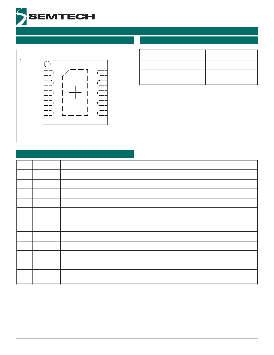
Ordering Information
Pin Configuration
n
i
P
e
m
a
N
n
i
P
n
o
i
t
c
n
u
F
n
i
P
1
N
I
V
.
e
g
a
tl
o
v
t
u
p
n
I
2
-
2
C
.
2
r
o
ti
c
a
p
a
c
t
e
k
c
u
b
f
o
l
a
n
i
m
r
e
t
e
v
it
a
g
e
N
3
D
N
G
.
s
a
i
v
e
l
p
it
l
u
m
g
n
i
s
u
e
n
a
l
p
d
n
u
o
r
g
o
t
t
c
e
n
n
o
c
-
d
n
u
o
r
G
4
-
1
C
.
1
r
o
ti
c
a
p
a
c
t
e
k
c
u
b
f
o
l
a
n
i
m
r
e
t
e
v
it
a
g
e
N
5
H
S
A
L
F
s
e
d
ir
r
e
v
o
o
s
l
a
d
n
a
h
g
i
h
n
e
h
w
e
d
o
m
h
s
a
l
F
e
v
it
c
a
n
i
e
c
i
v
e
d
e
h
t
s
t
u
p
-
n
i
p
e
l
b
a
n
e
e
d
o
m
h
s
a
l
F
.
L
R
T
C
6
T
E
S
I
.r
o
t
s
i
s
e
r
g
n
it
t
e
s
t
n
e
r
r
u
c
e
h
t
d
n
a
e
d
o
h
t
a
c
D
E
L
e
h
t
o
t
t
c
e
n
n
o
c
-
n
i
p
e
c
n
e
r
e
f
e
r
g
n
it
t
e
s
-
t
n
e
r
r
u
C
7
L
R
T
C
.
h
g
i
h
n
e
h
w
e
d
o
m
t
h
g
il
t
o
p
S
n
i
t
n
e
r
r
u
c
t
u
p
t
u
o
e
h
t
t
e
s
d
n
a
e
l
b
a
n
e
o
t
d
e
s
u
-
ti
b
t
u
p
n
i
l
o
r
t
n
o
C
8
+
1
C
.
1
r
o
ti
c
a
p
a
c
t
e
k
c
u
b
f
o
l
a
n
i
m
r
e
t
e
v
it
i
s
o
P
9
T
U
O
V
.
n
i
p
t
u
p
t
u
O
0
1
+
2
C
.
2
r
o
ti
c
a
p
a
c
t
e
k
c
u
b
f
o
l
a
n
i
m
r
e
t
e
v
it
i
s
o
P
T
l
a
m
r
e
h
T
d
a
P
e
l
p
it
l
u
m
g
n
i
s
u
e
n
a
l
p
d
n
u
o
r
g
o
t
t
c
e
n
n
o
C
.
y
ll
a
n
r
e
t
n
i
d
e
t
c
e
n
n
o
c
t
o
n
-
s
e
s
o
p
r
u
p
g
n
i
k
n
i
s
t
a
e
h
r
o
f
d
a
P
.
s
a
i
v
Pin Descriptions
E
C
I
V
E
D
E
G
A
K
C
A
P
T
R
T
L
M
I
5
1
6
C
S
)
1
(
3
x
3
0
1
-
D
P
L
M
)
2
(
B
V
E
5
1
6
C
S
d
r
a
o
B
n
o
it
a
u
l
a
v
E
Notes:
(1) Available in tape and reel only. A reel contains 3000 devices.
(2) Available in lead-free package only. This product is fully WEEE
and RoHS compliant.
TOP VIEW
1
2
3
4
10
9
8
7
5
6
MLP10: 3X3 10 LEAD
T
VIN
C2-
GND
C1-
FLASH
C2+
VOUT
C1+
CTRL
ISET

5
2005 Semtech Corp.
www.semtech.com
POWER MANAGEMENT
SC615
Applications Information
General Operation
The SC615 is a powerful 2X charge pump designed to
drive a high-intensity white LED with a constant current
(Spotlight mode) or with a pulsed current of higher inten-
sity (Flash mode) used for camera flash.
In Flash mode the SC615 output can drive 500mA at
4.25V into an LED for a minimum duration of 500ms.
The FLASH pin is used to trigger this mode (active high).
In spotlight mode the SC615 regulates the output cur-
rent to 100mA when the CTRL pin is pulled high and the
FLASH pin is low. Note that Flash mode has priority over
Spotlight mode, i.e., the FLASH pin triggers Flash mode
regardless of the state of the CTRL pin.
Output current is regulated by attaching the ISET pin to
the cathode(s) of the LED package and a low resistance
sense resistor (typically 0.5
). The ISET pin monitors
the voltage at the cathode and signals the charge pump
to increase or decrease the output current until the ISET
voltage reaches the programmed setting. The resistor
value is chosen to set the current through the LED based
on this reference voltage. The resistor can be chosen to
set either the flash mode current or spotlight mode cur-
rent, but it should not be less than 0.5
due to output
current limitations of the device.
Flash Mode
Flash mode is enabled whenever the FLASH pin is pulled
high and remains active until the FLASH pin is released.
This mode has higher priority than Spotlight mode, so
the state of the CTRL pin is overridden whenever the
FLASH pin is activated. While in flash mode the refer-
ence voltage on the ISET pin is set to 250mV. The dura-
tion of the pulse is limited by the amount of power that
can be dissipated in the SC615 before it exceeds the
maximum operating temperature. Note that if an output
current less than the rated 500mA is desired, the dura-
tion of the pulse can increase proportionally. However,
great care should be taken to insure the FLASH pin is
not held high for an extended amount of time so that
overheating does not occur. Extending flash mode be-
yond the 500ms pulse limit could adversely affect the
long term reliability of the SC615.
Spotlight Mode
Spotlight mode is enabled by setting the CTRL pin high
and keeping the FLASH pin low. When in Spotlight mode,
the SC615 can maintain a constant current indefinitely
to drive an LED or bank of LEDs. The ISET reference
voltage is set to 50mV so that the output current is main-
tained at 100mA when a 0.5
resistor is used.
Protection Circuitry
The SC615 also provides protection circuitry that pre-
vents the device from operating in an unspecified state.
These funtions include Input Over-Voltage Protection
(IOVP), Output Over-Voltage Protection (OVP), Over-Tem-
perature (OT) Protection, Over-Current Protection (OCP),
and Short-Circuit Current Protection (SCCP).
Input Over-Voltage Protection
Input over-voltage protection is included to prevent op-
eration at high input voltages that could damage the
device. The IOVP circuit senses the input voltage and
determines when the supply exceeds 6V. Hysteresis is
included in this circuit to avoid chattering between states.
When the voltage rises above this threshold, the device
is disabled until the input voltage drops to a level within
the specified range.
Output Over-Voltage Protection
Output over-voltage protection is included to prevent the
SC615 from generating an output voltage that could dam-
age other devices connected to it such as load LEDs and
bypass capacitors. When the output voltage exceeds
5.5V, the OVP circuit disables the charge pump until the
voltage decreases to a level within the acceptable range.
This circuit allows the device to drive LEDs with high for-
ward voltages at a reduced level without exceeding the
output voltage limits specified for the device. Note, how-
ever, that this effect is a consequence of the OVP circuit
and is not its intended purpose.
Over-Temperature Protection
The over-temperature circuit helps prevent the device
from overheating and experiencing a catastrophic fail-
ure. When the junction temperature exceeds 150∞C the
device is disabled. It remains disabled until the junction
temperature drops below this threshold. As with the UVLO
and OVP circuits, hysteresis is included to prevent tog-
gling between modes.

6
2005 Semtech Corp.
www.semtech.com
POWER MANAGEMENT
SC615
Over-Current Protection
When the SC615 is in 2X charge pump mode, the input
current will be approximately doubled the required out-
put. When the steady-state load requires the maximum
current available in 2X mode, the OCP circuit prevents
the device from overheating due to excessive power dis-
sipation.
Short-Circuit Current Protection
Short-circuit current protection is provided to limit the
current that can be sourced when the output is shorted
to ground. When a short circuit forces V
OUT
to drop below
2V, the SCCP detects the condition and limits the output
current.
Resistor Selection
The ISET resistor selection is critical in generating the
correct current. The value can be chosen to set the Spot-
light mode current or the Flash mode current, but it must
be noted that the two current settings are dependent on
the same resistor. It is recommended that the resistor
be selected to match the desired LED current for Flash
mode. This allows the designer to set the SC615's maxi-
mum current and select the package size necessary for
the power dissipation required in Flash mode. The typi-
cal application shown on page 1, uses a 0.5
resistor to
set a flash mode current of 500mA and spotlight mode
current of 100mA. A high precision resistor should be
used to ensure the specified accuracy for LED current.
To avoid malfunction of the charge pump, it is recom-
mended that the resistance seen at the ISET pin remain
constant while the device is active (Flash or Spotlight
mode). Changing the resistance value or the load cur-
rent while the device is active could cause instability that
would result in non-compliant behavior.
The load current return path is from the ISET sense point
through the resistor and back to the ground pins. Resis-
tance in this path adds to the total resistance and has
the effect of reducing the LED current by about 4% per
10mV of DC drop across the return copper trace in flash
mode. For this reason, it is crucial to have a low resis-
tance return path. Place and ground the resistor as close
as possible to the ground pin of the SC615. The trace
from the ISET pin has virtually no current. The ISET trace
should make contact at the pad of the power sense re-
sistor to minimize the effect of voltage drop between
the LED cathode and the resistor.
Capacitor Selection
The SC615 is designed to use low-ESR ceramic capaci-
tors for the input and output bypass capacitors as well
as the charge pump bucket capacitors. Ideal perfor-
mance is achieved when C1 is exactly equal to C2. It is
recommended that X5R or X7R ceramic capacitors be
used for best performance.
Thermal Resistance
The SC615 package is thermally efficient when the cir-
cuit board layout connects the thermal pad though mul-
tiple vias to the ground plane. The thermal resistance is
rated at 49∞C/W and this rating is dependent on the
connection between the thermal pad and the ground
plane. A layout that is done correctly should keep the
junction temperature below the OT limit while operating
the SC615 within the specified electrical conditions for
I
OUT
and V
ISET
. A poor layout may allow the junction tem-
perature to reach the OT limit while in Flash or Spotlight
mode. So, it is important to maintain adequate ground
plane around the device to maximize heat transfer to
the PCB.
Applications Information (Cont.)
7
2005 Semtech Corp.
www.semtech.com
POWER MANAGEMENT
SC615
Block Diagram
0.5
1
µF
1
µF
1
µF
10
µF
CHARGE
PUMP
VBAT
250kHz
Logic Control
Reference
Voltage
Generator
LDO
C1+
C1-
C2+
C2-
VOUT
ISET
VIN
CTRL
FLASH
GND
white LED
CTRL
FLASH
8
2005 Semtech Corp.
www.semtech.com
POWER MANAGEMENT
SC615
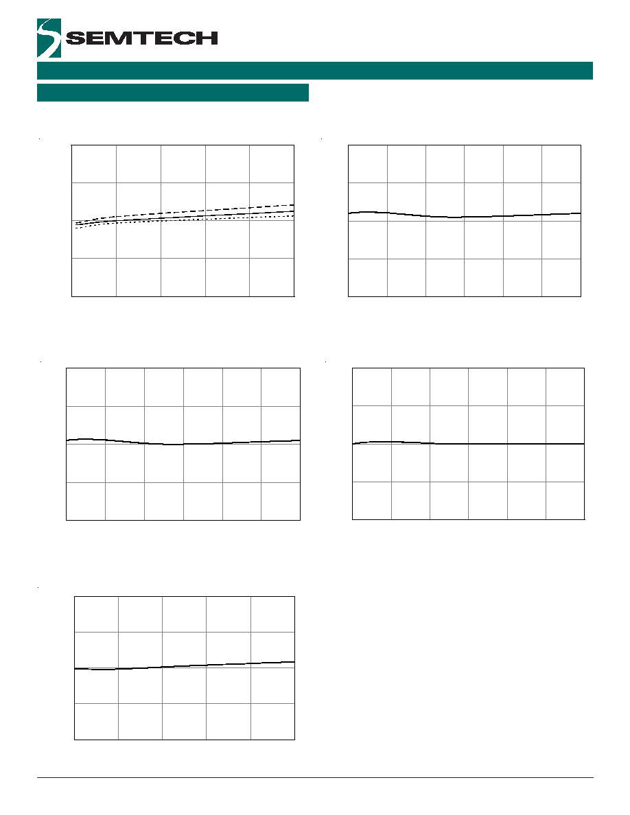
Typical Characteristics
Flash Duration
Flash Current at 500ms
Flash Current at 100ms
Flash Current at 10ms
VOUT = 3.53V(start) to 3.40V(LED heated 500ms)
VOUT = 3.4V
VOUT = 3.46V
VOUT = 3.53V
100mA Spotlight Current
VOUT = 2.93V
460
480
500
520
540
0
100
200
300
400
500
Pulse Duration [ms]
LE
D Cur
r
e
n
t [m
A]
VIN=4.2V
VIN=3.75V
VIN=3.3V
460
480
500
520
540
3.30
3.45
3.60
3.75
3.90
4.05
4.20
VIN [V]
Curr
e
n
t [
m
A]
460
480
500
520
540
3.30
3.45
3.60
3.75
3.90
4.05
4.20
VIN [V]
Cu
rre
nt [m
A]
460
480
500
520
540
3.30
3.45
3.60
3.75
3.90
4.05
4.20
VIN [V]
Curr
e
n
t
[m
A]
70.0
85.0
100.0
115.0
130.0
3.00
3.45
3.90
4.35
4.80
5.25
VIN [V]
Curr
e
n
t
[m
A]
9
2005 Semtech Corp.
www.semtech.com
POWER MANAGEMENT
SC615
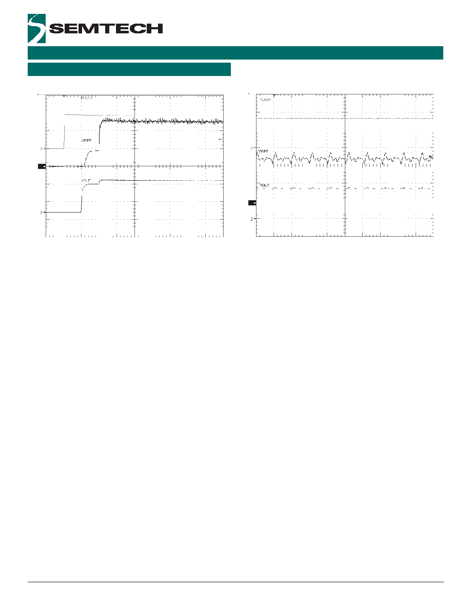
Ch1 100mV/div
Ch2 2V/div
Ch3 2V/div
40us/div
Startup Flash Mode 500mA
Ch1 100mV/div
Ch2 2V/div
Ch3 2V/div
4us/div
Flash Mode VISET Ripple
Typical Characteristics (Cont.)

10
2005 Semtech Corp.
www.semtech.com
POWER MANAGEMENT
SC615
Layout Guidelines
The following layout is suggested for a two-layer design.
The capacitors C1 and C2 are the bucket capacitors and
each conducts the full load current of up to 500mA
pulsed for one half clock cycle. C3 is the output
decoupling capacitor placed near the SC615 VOUT pin.
C4 is the input decoupling capacitor placed near the
SC615 VIN pin. Multiple vias should be used whenever
it is necessary to change layers on nets connecting to
pins VIN, VOUT, GND, C1-, C1+, C2- and C2+. Resistor
R1 is routed with a very low resistance connection be-
tween R1 and GND pin 3. The sense trace between Pin
6 and R1 is routed around the ground vias, allowing the
Bottom Copper
Top Copper
shortest ground return path possible. The sense trace is
connected to R1 at the positive terminal pad for the most
accurate output possible.
The bottom copper layer is mostly a ground plane with
no obstructions between the ground vias. The smaller
rectangle to the left connects the input power to VIN pin
1 and input capacitor C4. The two traces at the lower
left are for logic inputs FLASH and CTRL. The trace to
the right is the ISET pin "sense" trace. The sense trace is
routed out of the path of the returning ground current.
11
2005 Semtech Corp.
www.semtech.com
POWER MANAGEMENT
SC615
Outline Drawing -MLPD-10 3x3
Marking Diagram
MIN
aaa
bbb
b
e
L
N
D
C
E
A1
A2
A
DIM
MILLIMETERS
NOM
DIMENSIONS
MAX
NOM
INCHES
MIN
MAX
.114
.118
.122
2.90
3.00
3.10
-
-
-
-
(LASER MARK)
INDICATOR
PIN 1
1
N
2
NOTES:
CONTROLLING DIMENSIONS ARE IN MILLIMETERS (ANGLES IN DEGREES).
COPLANARITY APPLIES TO THE EXPOSED PAD AS WELL AS TERMINALS.
2.
1.
.003
.007
.042
10
.009
.048
-
.000
.031
(.008)
0.08
0.23
10
.011
.052
0.18
1.06
.039
-
.002
-
0.00
0.80
1.31
0.30
1.21
-
0.05
1.00
(0.20)
.004
0.10
0.50 BSC
.020 BSC
0.30
.012
.020
.016
0.40
0.50
A
aaa C
A2
SEATING
PLANE
A1
A
bxN
bbb
C A B
B
e
C
C
D
LxN
E
E
.074
.079
.083
1.87
2.02
2.12
615
yyww
Top Mark
xxxx
yyww = Datecode (Example = 0552)
xxxx = Semtech Lot Number

12
2005 Semtech Corp.
www.semtech.com
POWER MANAGEMENT
SC615
Land Pattern - MLPD-10 pin
.087
.055
2.20
1.40
.150
.020
.012
.037
3.80
0.30
0.95
0.50
(.112)
.075
1.90
(2.85)
K
H
X
THIS LAND PATTERN IS FOR REFERENCE PURPOSES ONLY.
CONSULT YOUR MANUFACTURING GROUP TO ENSURE YOUR
COMPANY'S MANUFACTURING GUIDELINES ARE MET.
NOTES:
1.
INCHES
DIMENSIONS
G
K
H
X
Y
P
Z
C
DIM
MILLIMETERS
Y
Z
G
(C)
P
Semtech Corporation
Power Management Products Division
200 Flynn Road, Camarillo, CA 93012
Phone: (805) 498-2111 FAX (805)498-3804
Contact Information
Visit us at:
www.semtech.com