1
www.semtech.com
5+&
Fully Integrated High Current
Lithium-Ion Battery Charger System
POWER MANAGEMENT
Revision 3, April 2003
Description
Features
Applications
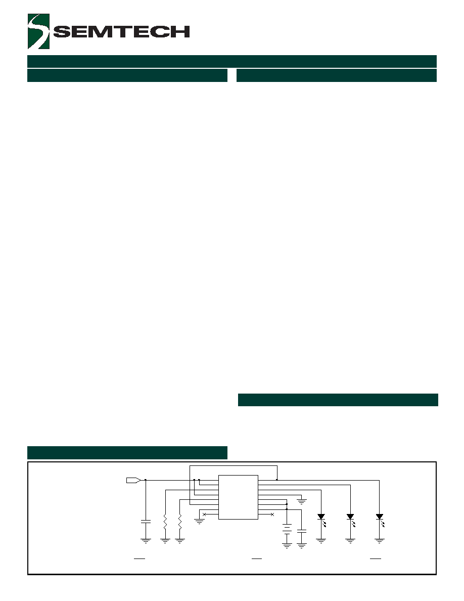
Typical Application Circuit
K
Fully integrated charger with FET pass transistor,
reverse-blocking diode, sense resistor and thermal
protection
K
4.1V, 4.2V & Adjustable Output Voltage
K
Programmable precharge, fastcharge & termination
current
K
Battery voltage controlled to 1% accuracy
K
Soft-start for step load and adaptor plug-in
K
Up to 1.5A continuous charge current
K
Charge current monitor output from microcontroller
or ADC Interface
K
Input voltages range from 4.2V to 14V
K
0.1�A Battery leakage in shutdown and monitor
modes
K
Operates without a battery in regulated LDO mode
K
Small 4mm x 4mm 16 lead MLP package
K
Low thermal impedance of 50�����C/watt
K
Few external components
K
Over current protection in all charging modes
K
Over voltage protection
K
All outputs able to drive LEDs and interface to host
processor
K
Remote Kelvin sensing at the battery terminal
K
Small input & output filter capacitors
K
Status output communicates charging and end of
charge cycle
K
Now Available in Lead-Free Packaging
K
Charges Li-Ion, Li-Polymer, NiCd and NiMH Batteries
K
Cellular phones
K
PDAs and Handheld computers
K
Handheld meters
K
Charging stations
K
Digital cameras
The SC801 is a fully integrated, single cell, constant-cur-
rent/constant-voltage Lithium-Ion\Li-Polymer battery
charger management system. The SC801 has built in in-
telligence and extreme functionality. When the battery
voltage is below 2.8V the charger operates in a pre-
charge mode with a charging current of up to 125mA
based on the ITERM pin resistor. This pre-charge mode is
set to limit power dissipation due to an undercharged
battery. When the battery voltage exceeds 2.8V, the
charger enters a fast charge mode. In this mode, the
SC801 delivers up to 1.5A to the battery based on the
IPRGM pin resistor.
The part also features current termination, ending the
charge cycle when the battery is charged and the charge
current drops below the current programmed by the
ITERM pin resistor. In addition, the charge current can
be monitored by the voltage on the IPRGM pin allowing a
microcontroller or ADC to access the current informa-
tion to determine when to externally terminate the charge
cycle. Once the charge cycle is complete and terminates,
the device enters the charge monitor mode where the
output voltage of the battery is monitored. If this voltage
drops below the recharge threshold the device will enter
the fast charge mode again, to bring the battery to its
fully charged state. Both the shutdown and monitor
modes drain no more than 1uA from the battery guaran-
teed.
The output voltage to the battery is controlled to within
1% of the programmed voltage for either 4.1V or 4.2V.
The SC801 can also function as a general purpose cur-
rent source or as a current source for charging nickel-
cadmium (NiCd) and nickel-metal-hydride (NiMH) batter-
ies using external termination.
C H A R G E R
F A U LT
B A TTE R Y
R 2
C H A R G E R V I N
S TA TU S
S C 80 1
1 4
1
3
7
4
1 5
9
1 0
2
1 1
5
8
1 3
6
1 6
1 2
V C C
B S E N
I P R G M
E N
I TE R M
V O U T
O V P
S TA T
V P R G M
C P
N C
B I P
V C C
G N D
V O U T
N C
P R E S E N T
C 2
2 . 2 uF
R 1
C 1
1 u F
88
R
1.5
Current
n
Terminatio
1000
R
1.5
Current
Charge
-
Fast
88
R
2.8
Current
Charge
-
Pre
2
1
2
�
=
�
=
�
=
2
2002 Semtech Corp.
www.semtech.com
5+&
POWER MANAGEMENT
Absolute Maximum Ratings
Electrical Characteristics
r
e
t
e
m
a
r
a
P
l
o
b
m
y
S
m
u
m
i
x
a
M
s
t
i
n
U
D
N
G
o
t
N
E
,
C
C
V
0
.
4
1
o
t
3
.
0
-
V
D
N
G
o
t
P
I
B
,
M
R
E
T
I
,
T
A
T
S
,
P
V
O
,
P
C
,
M
G
R
P
I
,
M
G
R
P
V
,
T
U
O
V
0
.
6
+
o
t
3
.
0
-
V
n
o
i
t
a
p
i
s
s
i
D
r
e
w
o
P
/
W
m
0
2
e
t
a
r
e
D
(
P
L
M
C
�
5
8
e
v
o
b
a
C
� )
P
D
5
.
2
W
D
N
G
o
t
t
r
o
h
s
T
U
O
V
s
u
o
u
n
i
t
n
o
C
t
n
e
i
b
m
A
o
t
n
o
i
t
c
n
u
J
,
e
c
n
a
t
s
i
s
e
R
l
a
m
r
e
h
T
A
J
0
5
*
W
/
C
�
e
r
u
t
a
r
e
p
m
e
T
n
o
i
t
c
n
u
J
g
n
i
t
a
r
e
p
O
T
J
0
5
1
C
�
e
r
u
t
a
r
e
p
m
e
T
d
a
e
L
T
D
A
E
L
5
3
2
C
�
s
d
n
o
c
e
s
0
1
)
g
n
i
r
e
d
l
o
S
(
e
r
u
t
a
r
e
p
m
e
T
e
g
a
r
o
t
S
T
G
T
S
0
5
1
o
t
5
6
-
C
�
)
l
e
d
o
M
y
d
o
B
n
a
m
u
H
(
g
n
i
t
a
R
D
S
E
D
S
E
2
V
k
r
e
t
e
m
a
r
a
P
l
o
b
m
y
S
s
n
o
i
t
i
d
n
o
C
C
�
5
2
T
A
0
4
-
(
�
5
8
+
o
t
C
�
)
C
s
t
i
n
U
n
i
M
p
y
T
x
a
M
n
i
M
x
a
M
e
g
a
t
l
o
V
t
u
p
n
I
C
C
V
2
.
4
4
1
V
e
g
a
t
l
o
V
g
n
i
t
a
r
e
p
O
V
P
O
2
.
4
5
.
6
V
t
n
e
r
r
u
C
g
n
i
t
a
r
e
p
O
I
C
C
e
d
o
M
g
n
i
g
r
a
h
C
A
�
0
=
P
C
,
S
U
T
A
T
S
,
P
V
O
2
A
m
e
d
o
M
O
D
L
A
�
0
=
P
C
,
S
U
T
A
T
S
,
P
V
O
5
2
t
n
e
r
r
u
C
e
g
a
k
a
e
L
y
r
e
t
t
a
B
I
T
U
O
V
V
0
=
C
C
V
1
.
0
1
A
�
e
g
a
t
l
o
V
d
e
t
a
l
u
g
e
R
V
T
A
B
V
M
G
R
P
h
g
i
H
c
i
g
o
L
=
V
M
G
R
P
w
o
L
c
i
g
o
L
=
0
2
.
4
0
1
.
4
6
1
.
4
6
0
.
4
4
2
.
4
4
1
.
4
V
k
c
a
b
d
e
e
F
e
d
o
M
t
s
u
j
d
A
e
g
a
t
l
o
V
V
M
G
R
P
r
e
d
i
v
i
D
l
a
n
r
e
t
x
E
=
V
C
C
V
5
.
6
-
V
2
.
4
=
0
.
3
7
9
.
2
3
0
.
3
V
t
n
e
r
r
u
C
e
g
r
a
h
C
-
e
r
P
y
r
e
t
t
a
B
P
I
C
I
M
R
E
T
k
1
0
.
3
=
R
r
o
t
s
i
s
e
R
V
Y
R
E
T
T
A
B
V
5
.
2
>
2
8
2
7
2
9
A
m
t
n
e
r
r
u
C
n
o
i
t
a
n
i
m
r
e
T
y
r
e
t
t
a
B
I
M
R
E
T
5
4
8
3
2
5
t
n
e
r
r
u
C
e
g
r
a
h
C
-
t
s
a
F
y
r
e
t
t
a
B
F
I
C
I
M
G
R
P
k
1
0
.
3
=
I
M
G
R
P
k
7
8
.
1
=
V
Y
R
E
T
T
A
B
V
8
.
3
=
V
m
0
5
5
=
e
g
a
t
l
o
V
t
u
o
p
o
r
D
0
0
5
0
0
8
0
5
4
0
5
7
0
5
5
0
5
8
A
m
Unless otherwise noted: VCC = 4.75V - 5.25V
Exceeding the specifications below may result in permanent damage to the device, or device malfunction. Operation outside of the parameters
specified in the Electrical Characteristics section is not implied.
* Tied to PCB with 1 Square Inch, 2 Ounce Copper

3
2002 Semtech Corp.
www.semtech.com
5+&
POWER MANAGEMENT
Electrical Characteristics Cont.
r
e
t
e
m
a
r
a
P
l
o
b
m
y
S
s
n
o
i
t
i
d
n
o
C
C
�
5
2
T
A
o
t
C
�
0
4
-
(
)
C
�
5
8
+
s
t
i
n
U
n
i
M
p
y
T
x
a
M
n
i
M
x
a
M
e
g
r
a
h
C
-
t
s
a
F
y
r
e
t
t
a
B
t
i
m
i
L
t
n
e
r
r
u
C
V
<
V
8
.
2
Y
R
E
T
T
A
B
V
<
T
A
B
V
1
=
e
g
a
t
l
o
v
t
u
o
p
o
r
D
*
*
5
.
1
A
I
G
O
R
P
e
g
a
t
l
o
V
d
e
t
a
l
u
g
e
R
5
.
1
4
.
1
6
.
1
V
V
N
I
d
l
o
h
s
e
r
h
T
g
n
i
s
i
R
O
L
V
U
2
.
4
3
.
4
V
d
l
o
h
s
e
r
h
T
e
d
o
M
t
s
u
j
d
A
e
g
a
t
l
o
V
0
9
V
m
V
T
A
B
d
l
o
h
s
e
r
h
T
e
g
r
a
h
c
e
r
P
8
.
2
7
.
2
9
.
2
V
V
T
A
B
d
l
o
h
s
e
r
h
T
e
g
r
a
h
c
e
R
V
T
A
B
V
-
Y
R
E
T
T
A
B
0
0
2
0
7
1
0
2
2
V
m
V
N
I
d
l
o
h
s
e
r
h
T
g
n
i
s
i
R
P
V
O
8
.
6
5
2
5
.
6
1
.
7
V
V
N
I
d
l
o
h
s
e
r
h
T
g
n
il
l
a
F
P
V
O
5
.
6
2
.
6
8
.
6
V
V
N
I
s
i
s
e
r
e
t
s
y
H
P
V
O
0
0
3
0
0
2
0
0
4
V
m
n
w
o
d
t
u
h
S
e
r
u
t
a
r
e
p
m
e
T
r
e
v
O
C
�
0
1
=
s
i
s
e
r
e
t
s
y
H
5
6
1
C
�
t
n
e
r
r
u
C
e
c
r
u
o
S
t
u
p
t
u
O
s
u
t
a
t
S
e
g
r
a
h
C
-
t
s
a
F
r
o
e
g
r
a
h
C
-
e
r
P
V
8
.
2
=
T
A
T
S
V
0
1
A
m
V
5
2
.
0
=
T
A
T
S
V
,
e
g
r
a
h
C
f
o
d
n
E
1
A
m
,
e
d
o
m
O
D
L
r
o
r
o
t
p
a
d
A
o
N
e
c
n
a
d
e
p
m
I
h
g
i
H
1
A
�
t
n
e
r
r
u
C
e
c
r
u
o
S
t
u
p
t
u
O
P
V
O
P
V
O
>
C
C
V
0
1
A
m
t
n
e
r
r
u
C
e
c
r
u
o
S
t
u
p
t
u
O
P
C
O
L
V
U
>
C
C
V
0
1
A
m
e
g
a
k
a
e
L
t
u
p
n
I
E
S
N
E
S
B
t
n
e
r
r
u
C
1
.
0
1
A
�
s
t
u
p
t
u
O
P
C
,
P
V
O
,
T
A
T
S
V
H
O
A
m
0
1
=
d
a
o
L
4
.
2
V
A
m
1
=
d
a
o
L
6
.
2
V
L
O
A
�
0
0
5
-
=
d
a
o
L
5
2
.
0
V
s
t
u
p
n
I
M
G
R
P
V
,
P
I
B
,
N
E
V
H
I
8
.
1
V
V
L
I
4
.
0
V
** Thermally Limited
Unless otherwise noted: VCC = 4.75V - 5.25V

4
2002 Semtech Corp.
www.semtech.com
5+&
POWER MANAGEMENT
Pin Configuration
Ordering Information
Pin Descriptions
#
n
i
P
e
m
a
N
n
i
P
n
o
i
t
c
n
u
F
n
i
P
1
N
E
S
B
t
o
n
o
D
.
e
g
a
t
l
o
v
y
r
e
t
t
a
b
e
s
n
e
s
n
i
v
l
e
K
o
t
l
a
n
i
m
r
e
t
y
r
e
t
t
a
b
o
t
t
c
e
n
n
o
C
.
n
i
p
e
s
n
e
s
e
g
a
t
l
o
v
y
r
e
t
t
a
B
.
g
n
i
t
a
o
l
f
n
i
p
s
i
h
t
e
v
a
e
l
2
M
G
R
P
V
.
e
l
b
a
t
s
u
j
d
a
=
r
o
t
s
i
s
e
R
.
V
2
.
4
=
h
g
i
h
c
i
g
o
L
.
V
1
.
4
=
w
o
l
c
i
g
o
L
.
n
i
p
m
a
r
g
o
r
p
e
g
a
t
l
o
v
e
l
b
a
t
c
e
l
e
S
3
M
G
R
P
I
m
a
r
g
o
r
p
o
t
d
n
u
o
r
g
o
t
r
o
t
s
i
s
e
r
a
s
e
r
i
u
q
e
R
.
e
d
o
m
e
g
r
a
h
c
t
s
a
f
n
i
n
i
p
m
a
r
g
o
r
p
t
n
e
r
r
u
c
r
e
g
r
a
h
C
.
t
n
e
r
r
u
c
e
g
r
a
h
c
-
t
s
a
f
4
M
R
E
T
I
o
t
d
n
u
o
r
g
o
t
r
o
t
s
i
s
e
r
a
s
e
r
i
u
q
e
R
.
t
n
e
r
r
u
c
e
g
r
a
h
c
-
e
r
p
d
n
a
n
o
i
t
a
n
i
m
r
e
t
t
n
e
r
r
u
c
r
o
f
n
o
i
t
c
e
l
e
S
.
t
n
e
r
r
u
c
n
o
i
t
a
n
i
m
r
e
t
d
n
a
e
g
r
a
h
c
-
e
r
p
m
a
r
g
o
r
p
5
C
N
t
c
e
n
n
o
C
o
N
6
D
N
G
d
n
u
o
r
G
7
N
E
.
e
c
i
v
e
d
s
e
l
b
a
s
i
d
w
o
l
c
i
g
o
L
.
e
c
i
v
e
d
s
e
l
b
a
n
e
h
g
i
h
c
i
g
o
L
.
n
i
p
e
l
b
a
s
i
d
/
e
l
b
a
n
e
e
c
i
v
e
D
8
P
I
B
h
g
i
h
c
i
g
o
L
.
e
c
a
l
P
n
I
y
r
e
t
t
a
B
s
l
a
n
g
i
s
t
a
h
t
r
e
ll
o
r
t
n
o
c
o
r
c
i
m
r
o
y
r
t
i
u
c
r
i
c
l
a
n
r
e
t
x
e
m
o
r
f
d
e
v
i
r
e
d
t
u
p
n
I
o
D
.
e
d
o
m
O
D
L
o
t
n
i
e
c
i
v
e
d
s
t
u
p
w
o
l
c
i
g
o
L
.
e
d
o
m
g
n
i
g
r
a
h
c
n
i
d
n
a
e
c
a
l
P
n
I
y
r
e
t
t
a
B
s
e
t
a
c
i
d
n
i
.
g
n
i
t
a
o
l
f
n
i
p
s
i
h
t
e
v
a
e
l
t
o
n
9
P
V
O
.
A
m
0
1
e
c
r
u
o
S
n
a
c
n
i
p
s
i
h
T
V
5
.
6
n
a
h
t
r
e
h
g
i
h
s
i
e
g
a
t
l
o
v
t
u
p
n
i
r
e
g
r
a
h
c
f
i
g
a
l
f
t
l
u
a
f
e
g
a
t
l
o
v
r
e
v
O
0
1
T
A
T
S
n
i
n
e
h
W
.
)
w
o
L
(
e
g
r
a
h
c
f
o
d
n
e
d
n
a
)
h
g
i
H
(
e
g
r
a
h
c
t
s
a
F
,
)
h
g
i
H
(
e
g
r
a
h
c
-
e
r
P
:
n
i
P
s
u
t
a
t
S
r
e
g
r
a
h
C
.
A
m
0
1
e
c
r
u
o
s
n
a
c
n
i
p
s
i
h
T
.
e
c
n
a
d
e
p
m
i
h
g
i
h
s
i
n
i
p
s
i
h
t
e
d
o
m
O
D
L
1
1
P
C
e
h
t
f
o
s
s
e
l
d
r
a
g
e
r
s
n
i
p
C
C
V
e
h
t
o
t
r
e
w
o
p
s
i
e
r
e
h
t
n
e
h
w
h
g
i
h
c
i
g
o
l
,
r
o
t
a
c
i
d
n
i
t
n
e
s
e
r
p
r
e
g
r
a
h
C
.
A
m
0
1
e
c
r
u
o
s
n
a
c
n
i
p
s
i
h
T
.
e
t
a
t
s
n
i
p
e
l
b
a
n
E
2
1
C
N
t
c
e
n
n
o
C
o
N
3
1
C
C
V
.
r
e
w
o
p
r
o
t
p
a
d
a
o
t
t
c
e
n
n
o
c
,
n
i
p
y
l
p
p
u
S
4
1
C
C
V
.
r
e
w
o
p
r
o
t
p
a
d
a
o
t
t
c
e
n
n
o
c
,
n
i
p
y
l
p
p
u
S
5
1
T
U
O
V
.
y
r
e
t
t
a
b
o
t
t
c
e
n
n
o
c
,
t
u
p
t
u
o
r
e
g
r
a
h
C
6
1
T
U
O
V
.
y
r
e
t
t
a
b
o
t
t
c
e
n
n
o
c
,
t
u
p
t
u
o
r
e
g
r
a
h
C
E
C
I
V
E
D
)
1
(
E
G
A
K
C
A
P
R
T
L
M
I
1
0
8
C
S
6
1
P
L
M
T
R
T
L
M
I
1
0
8
C
S
)
2
(
6
1
P
L
M
B
V
E
1
0
8
C
S
)
3
(
d
r
a
o
B
n
o
i
t
a
u
l
a
v
E
Notes:
(1) Only available in tape and reel packaging. A reel con-
tains 3,000 devices.
(2) TRT extension designates the lead-free leadframe
package option.
(3) Specify the desired IC part number when ordering.
MLP16: 4X4 16 LEAD
TOP VIEW
BIP
EN
GND
NC
CP
STAT
12
11
10
9
NC
OVP
8
7
6
5
1
2
3
4
BSEN
VPRGM
IPRGM
ITERM
13
14
15
16
VCC
VCC
VOUT
VOUT
5
2002 Semtech Corp.
www.semtech.com
5+&
POWER MANAGEMENT
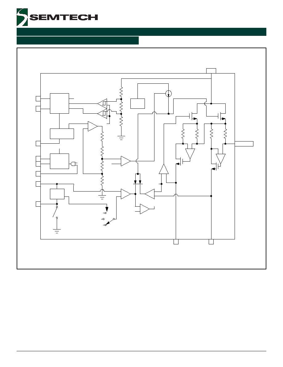
Block Diagram
+
-
+
-
+
-
+
-
+
-
+
-
+
-
+
-
Control
EN
1.2V
Reference
and OT SD
EN
Status
T
e
r
m
i
n
a
t
i
o
n
Vprog
Detect
UV
OV
1.2V
4.2V
4.1V
3.0V
Vout
V_FB
4.2V
4.1V
3.0V
1.2V
Termination
1.2V
Charge
Pump
Fast Charge
Enable
100
1
100
0.1
EN
OVP
GND
STAT
BIP
BSEN
VPRGM
ITERM
IPRGM
VOUT
VCC
CP
7
9
6
10
11
8
1
2
4
3
15,16
13,14

6
2002 Semtech Corp.
www.semtech.com
5+&
POWER MANAGEMENT
Monitor Mode
In the monitor mode the voltage of the battery will be
monitored against the programmed voltage. This will oc-
cur after a battery has been fully charged and the device
has shut off. If the voltage of the battery falls below the
recharge threshold (specified at 200mV) the charger will
activate and charge the battery to its programmed volt-
age. This means that it will enter the full charging se-
quence from fast-charge to terminating the charging cycle
when the programmed termination current is reached.
The maximum current drain of the battery during moni-
tor mode will be no more than 1uA over temperature.
LDO Mode
One of the nice features of the SC801 is its ability to
work with or without a battery. If the battery is not in
place the device can enter the LDO mode. In this mode
the SC801 will act like a low dropout regulator. The out-
put voltage is set to 4.1V, 4.2V or externally set by a
resistor divider. See the section titled Configuring the
Output Voltage to the Battery for setting an output volt-
age other than 4.1V or 4.2V. The input pin BIP (Battery
In Place) is used to switch the SC801 from charger mode
to LDO mode. If this pin is logic high the device will be in
charger mode, if it is logic low it will be in the LDO mode.
During LDO mode the device will regulate the output volt-
age with a current limit set by the resistor tied to the
IPRGM pin. The BIP pin can be tied to the CP pin to place
the device in charge mode whenever the adaptor is in
place. The maximum voltage on the BIP input pin is 6V,
so do not tie it to the VCC input since this voltage can
exceed 6V in some conditions. The BIP pin should never
be left floating, but instead, should be tied through pull-
up/pull-down resistors when connected to a high imped-
ance control pin, otherwise it can be connected directly
to the CP pin or GND. The equation for setting the cur-
rent limit in the LDO mode will be:
1000
R
1.5
ILDO
PRGM
�
=
LED Flags
There are three LED drivers on the SC801: OVP (Over
Voltage), STAT (Status) and CP (Charger Present). Each
output can drive an LED directly without a current limit
resistor. In addition, each output can be monitored by a
microprocessor for change in their status. The table above
defines each LED output.
Applications Information
Pre-Charge Mode
Pre-charge mode is automatically enabled whenever the
battery voltage is below 2.8V. It is primarily used to limit
the power dissipation of the battery and the SC801 de-
vice whenever the battery is undercharged. As the bat-
tery begins to charge in this mode, the voltage of the
battery will rise and when the 2.8V limit is reached, the
SC801 will switch to the fast charge mode. The pre-
charge current value is selected by the termination re-
sistor on the ITERM pin. The maximum range of the pre-
charge current is from 10mA to 125mA. Whenever the
charger is in pre-charge or fast-charge the status LED
will light indicating that the battery is being charged. The
equation to select the pre-charge current is given by:
88
R
2.8
PCI
TERM
�
=
Fast-Charge Mode
The fast-charge mode exists while the battery voltage is
above 2.8V and the battery is not fully charged. The fast-
charge current can be set to a maximum of 1.5A and is
selected by the program resistor on the IPRGM pin. In
fact, the voltage on this pin will represent the current
through the battery enabling a microprocessor or ana-
log-to-digital converter (ADC), to monitor battery current
by sensing the voltage on the IPRGM pin. The equation
to set the fast-charge current is given by:
1000
R
1.5
FCI
PRGM
�
=
Note that for a given program resistor the current through
the battery can be determined by replacing 1.5 with the
actual voltage on the IPRGM pin in the above equation.
Termination Current
Once the battery reaches the program voltage of 4.1V,
4.2V or externally set voltage, the device will transition
from a constant current source to a constant voltage
source, as the current through the battery begins to de-
crease while the voltage remains constant. During this
time when the current falls below the programmed ter-
mination current set by the termination resistor on the
ITERM pin, the SC801 will turn off and the end of charge
will be indicated by the status LED turning off. The equa-
tion to set the termination current is given by:
88
R
1.5
ITERM
TERM
�
=
7
2002 Semtech Corp.
www.semtech.com
5+&
POWER MANAGEMENT
Applications Information (Cont.)
The CP output can be used for a UVLO indicator. Regard-
less of the state of EN, the CP output reflects the volt-
age of the VCC (adapter) input. When VCC is above UVLO,
CP is high, 2.8V. When VCC is below UVLO, CP is low, 0V.
The CP pin can also put the device into the charge mode
whenever the adaptor has power, by connecting it to the
BIP pin.
The OVP LED will light whenever the SC801 is enabled
and there is an overvoltage on the VCC pins. When this
occurs the SC801 will turn off and stay off as long as the
overvoltage condition remains. As soon as the overvolt-
age is removed the SC801 will resume operation. The
OVP LED will not light if the part is disabled, even though
an overvoltage is present on the VCC pins.
Configuring the Output Voltage to the Battery
The battery voltage is set by the VPRGM pin. If this pin is
logic high the output voltage is set to 4.2V. If this pin is
logic low the output voltage will be set to 4.1V. The VPRGM
pin can be tied to the CP pin for 4.2V operation and ground
for 4.1V operation. For a value other than 4.1V or 4.2V a
resistor divider is required. This divider is set between
the VOUT pin and the VPRGM pin with the divider tap
connected to the BSEN pin. The schematic for such a
connection and the equation to set the output voltage is
given in Figure 1. The output voltage for Figure 1 will be
set to 4.77V with the resistors shown. The capacitor C1
may be needed for stability and or reduced ripple volt-
age. It is advisable to leave room on the PCB for adding
this capacitor, since it can be left out if it is not needed.
The evaluation board does have a place for the resistor
divider and capacitor to allow an adjustable voltage to
be set on this board via R1, R2 and C2 (see schematic
on page 10). With JP7 removed, jumper JP2 should be
added to complete the changes required for adjustable
mode operation on the evaluation board. For further
evaluation board information, see the section tilted Evalu-
ation Board.
S C 8 0 1
1 4
1
3
7
4
1 5
9
1 0
2
1 1
5
8
1 3
6
1 6
1 2
V C C
B S E N
I P R G M
E N
I TE R M
V O U T
O V P
S TA T
V P R G M
C P
N C
B I P
V C C
G N D
V O U T
N C
P R E S E N T
+5 V
B A TTE R Y
C 2
1 u F
C 1
3 3 0 p F
F A U L T
R 4
5 9 K
R 3
1 0 0 K
C H A R G E R
S TA TU S
C 3
2 . 2 u F
R 1
R 2
3.0
R3
R4
1
VOUT
�
+
=
FIGURE 1
Remote Kelvin Sensing at the Battery
Another nice feature of the SC801 is its ability to sense
the battery voltage directly at the battery with its Kelvin
BSEN pin. This allows the designer great flexibility in PCB
layout and achieves a much greater accuracy in sensing
the battery voltage where it counts, at the battery termi-
nals! Therefore, when laying out the PCB the designer
should route the BSEN pin directly to the terminal at which
the battery gets connected. In addition, in the LDO mode,
the BSEN pin will still need to sense the output voltage.
In LDO mode, the BSEN pin becomes the regulation feed-
back for the control-loop. In this case it is sensing the
output voltage of itself, since the battery is not in place.
Therefore BSEN should never be left floating.....
Capacitor Selection
Input and output capacitors can be low cost ceramic type.
The output capacitance range is 1uF to 4.7uF. The input
capacitor should be between 0.1uF to 1uF.
Overcurrent and Temperature Protection
Overcurrent protection is inherent to the SC801. The
SC801 operates as a current source and the output cur-
rent is limited by the mode it is in at the time. If in the
fast-charge mode the current is limited by the IPRGM
resistor, the fast-charge current. When the output volt-
age is less than 2.8V, the current is limited by the ITERM
resistor, the pre-charge current. Both of these functions
protect the device in an event of a short circuit condition
on the output. In the LDO mode the current is limited to
the fast-charge current, provided there is voltage on the
output. Under a short circuit condition in the LDO mode
the current will enter a hiccup mode. The temperature
shutdown can protect the device in conditions of excess
current as well, by shutting down the device when its die
temperature exceeds 165
o
C.
G
A
L
F
D
E
L
N
O
F
F
O
H
G
I
H
E
C
N
A
D
E
P
M
I
P
C
C
C
V
O
T
R
E
W
O
P
S
N
I
P
O
T
R
E
W
O
P
O
N
S
N
I
P
C
C
V
X
P
V
O
-
R
E
V
O
C
C
V
E
G
A
T
L
O
V
E
G
A
T
L
O
V
C
C
V
L
A
M
R
O
N
X
T
A
T
S
Y
R
E
T
T
A
B
G
N
I
G
R
A
H
C
Y
L
L
U
F
Y
R
E
T
T
A
B
D
E
G
R
A
H
C
E
D
O
M
O
D
L

8
2002 Semtech Corp.
www.semtech.com
5+&
POWER MANAGEMENT
Applications Information (Cont.)
Using the SC801 With a Charge Controller IC
The SC801 can also be used with numerous charge con-
troller ICs on the market. In many instances the charge
controller will control the charging and termination of the
SC801. The best method of interfacing the SC801 with
such a device is to place the SC801 in LDO mode, and
monitor the current to the battery by an ADC that
samples the voltage on the IPRGM pin. Slow and fast
charge can be controlled by placing two resistors in se-
ries from IPRGM to GND and adding a transistor switch
across one of the resistors. This way the current can be
monitored for proper termination by the charge control-
ler. In LDO mode the STAT LED will not light. When charg-
ing the battery in LDO mode the charge profile will be the
same as in charge mode except there will be no precharge
or termination current function. Meanwhile, the maxi-
mum current the battery will see is set by the battery
equivalent circuit or the fast-charge current limit. The
battery will still charge in this mode, albeit a slightly dif-
ferent approach than placing the charger in the charge
mode.
Evaluation Board
The evaluation board is shown on Page 10. The evalua-
tion board was designed to test the complete operation
of the SC801 and the SC801M. Note the minimum parts
requirement is shown within the dotted rectangle on the
schematic. The adaptor voltage of 5V is applied to TP1
and TP2 which supplies power to the SC801. The output
charger voltage or LDO output voltage is taken off of
TP4 and TP5. Jumper JP5 will set the device in LDO mode
when inserted or charge mode when left open. Jumper
JP6 will enable the device when inserted or disable the
device when left open. Note as long as power is applied
to VCC the CP LED will light, regardless of the EN pin
level. Jumper JP4 is used to measure the bias current of
the SC801 and should always be in place except when
measuring bias current. JP1 and JP3 set the charge limit
voltage to 4.2V or 4.1V respectively. Only one of these
jumpers JP1 or JP3 should be in place at any given time.
If you expect VCC to exceed 6V (testing breakdown of
the SC801) and you want to set the output voltage to
4.2V you should remove any jumper on JP1 and manu-
ally tie pin 2 of JP1 to the CP pin, because the absolute
maximum voltage on the VPRGM input pin is 6V. Jumper
JP7 when inserted will short the BSEN line to Vout for
charging Lithium-Ion batteries. Jumper JP2 should be in-
serted when an adjustable voltage is required, with the
addition of R1, R2 & C2. For more information about
selection of an adjustable voltage see the section titled,
Configuring the Output Voltage to the Battery. Note, only
one of these jumpers JP2 or JP7 should be inserted at
any given time. Jumper JP8 should be left open and is
used only for testing SC801M operation. Connector J1
is used for connecting the evaluation board to a demon-
stration platform to exemplify the SC801 operation. Other
components on the eval board consist of Semtechs
SD12 and SD05 ESD clamp diodes which should be part
of any system requiring ESD protection. LEDs for status
information and TP3 which will allow the current through
the battery to be monitored. The input capacitor C1 is
chosen to be 10uF to decouple any inductance from a
laboratory supply when evaluation is taking place.
Complete Charge Cycle
The complete charge cycle of the SC801 is shown on
page 15. The pre-charge current will be under control
until the precharge threshold of 2.8V is reached. At this
time the device enters the fast-charge mode and the
output voltage continues to increase as the constant
current is applied to the battery. Eventually constant volt-
age is reached and the current begins to decrease until
the termination current threshold is reached at which
time the SC801 will turn off. Many Lithium-Ion batteries
have a built in under-voltage detect circuit. This makes
the battery pack open circuited when the battery volt-
age falls below 3V typically. With these batteries the
SC801 will unlikely enter pre-charge operation because
the battery voltage will always be above 2.8V.

9
2002 Semtech Corp.
www.semtech.com
5+&
POWER MANAGEMENT
Applications Information (Cont.)
Layout Guidelines
Try to keep the traces from the adaptor input to the VCC
pins as wide as possible, to eliminate any voltage drop
across the device input traces. You want to make sure
the input-to-output voltage differential of the device does
not approach the dropout voltage. A curve of the drop-
out voltage vs. output current is shown on page 15. Any
voltage dropped over the input traces from the adaptor
will reduce the dropout voltage margin.
Make the high current output trace from the VOUT pins
as wide as possible. The BSEN line should be used prop-
erly to compensate for any voltage drops from the out-
put trace to the battery. Make a Kelvin connection with
the BSEN trace to where VOUT connects the battery ter-
minals. This is done by taking the BSEN trace and tying it
to the VOUT trace as close to the battery terminals as
possible. This way, any voltage drop across the trace re-
sistance to the battery will be compensated for because
BSEN will regulate the device output voltage (VOUT) at
the point it connects to the VOUT trace. If you tie the
BSEN line to the VOUT pin at the device you will eliminate
the benefit of its purpose and the trace resistance drop
will not be compensated. Therefore, it is best to have
the BSEN trace follow in parallel the VOUT trace and tie
them together at the contact point of the battery termi-
nal for the best result.
The bottom of the SC801 package has a heat slug and
this slug should be tied to a ground plane of the PCB
through one large via or a series of smaller vias. If there
is no ground plane, an area should be dedicated on the
bottom of the PCB to act as a heat sink. The evaluation
board has 1 square inch of copper and allows an output
current of greater that 1A. The more copper tied to this
slug the greater the output current available before ther-
mal limitations dominate. The two pins that are labeled
NC are not connected to the die. Therefore, tying these
pins to the ground plane offers no aide in heat removal
and has no electrical benefit.
10
2002 Semtech Corp.
www.semtech.com
5+&
POWER MANAGEMENT
Evaluation Board Schematic
TP 2
G N D
1
J P 2
A d jus t a b le V ou t
1
2
TP 1
+5 V I N
1
D 4
F A U L T
C 2
O P E N
J P 4
B I A S
1
2
J P 5
C H G R / L D O
1
2
D 1
S D 12
+
C 1
1 0 uF / 25 V
D 3
C P
R 1
O P E N
J P 1
4 . 2 V
1
2
C 4
2 . 2 uF
C 3
0 . 1 uF
TP 5
G N D
1
J P 3
4 . 1 V
1
2
D 2
S D 05
J 1
C O N 16 A P
1
3
5
7
9
1 1
1 3
1 5
2
4
6
8
1 0
1 2
1 4
1 6
+
+
+
+
+
+
+
+
+
+
+
+
+
+
+
+
J P 8
S C 80 1 / S C 8 01 M
1
2
R 2
O P E N
R 6
3 . 0 1K
R 4
1 M
TP 4
V O U T / V C H G
1
R 7
6 1 9
U 1
S C 80 1
1 4
1
3
7
4
1 5
9
1 0
2
1 1
5
8
1 3
6
1 6
1 2
V C C
B S E N
I P R G M
E N
I TE R M
V O U T
O V P
S TA T
V P R G M
C P
N C
B I P
V C C
G N D
V O U T
N C
J P 7
L i-I on
1
2
TP 3
I S E N S E
1
D 5
S TA TU S
R 3
1 0 K
J P 6
E N A B L E / D I S A B L E
1
2
MINIMUM PARTS REQUIREMENT WITHIN DOTTED LINE
R 5
1 . 2 4K
Top Gerber
Evaluation Board Gerber Plots
Bottom Gerber
Inner Gerber
Silk Screen Gerber
11
2002 Semtech Corp.
www.semtech.com
5+&
POWER MANAGEMENT
LDO Mode Timing Diagram
LDO Mode
LDO Mode
Vcc
Vout
CP
OVP
Stat
BIP
EN
1ms
Iout
High Z
Precharge
Limit
I
LIMIT
4.2V
6.5V
4.2V
6.3V
4ms
1ms
I
LIMIT
Low
Soft Start
1ms 1ms
4ms
5V
1ms
12
2002 Semtech Corp.
www.semtech.com
5+&
POWER MANAGEMENT
Charge Mode Timing Diagram
Charge Mode
Charge Mode
Vcc
Vout
CP
OVP
Stat
BIP
EN
Iout
Precharge
Limit
1ms
4.2V
Icharge
End of Charge
2.8V
4.2V
4ms
Soft Start
1ms
precharge
1ms
Monitor
Mode
4ms
Charge Mode
Charge Mode
1ms
4.0V
Termination
Current
13
2002 Semtech Corp.
www.semtech.com
5+&
POWER MANAGEMENT
Shutdown Mode
Vout/Iout off
CP,STAT,OVP Low
VBAT > 2.8V
Soft Start
Fast Charge Mode
VOUT=CV
Start Pre-Charge
VOUT=CV
VBAT>2.8V
IOUT < ITERM
Monitor Mode
STAT=Low
Vout off
VBAT = CV-200mv
Yes
Yes
Yes
Yes
Yes
Vin > UVLO
Yes
Iout=1500/Rprog
Iout=280/Rterm
Start CV Mode
Yes
BIP High
Over Voltage, Under
Voltage, or Over
Temperature will
force the SC801 into
Shutdown Mode from
any state.
En = High
And
Tj<Over Temp SD
CP Output = High
Charge Mode
STAT=High,
LDO Mode
STAT=High Z,
Iou t > 1500/Rprog
LDO Current Limit
Iou t = 1500/Rprog
VOUT=CV ?
Yes
Yes
State Diagram
14
2002 Semtech Corp.
www.semtech.com
5+&
POWER MANAGEMENT
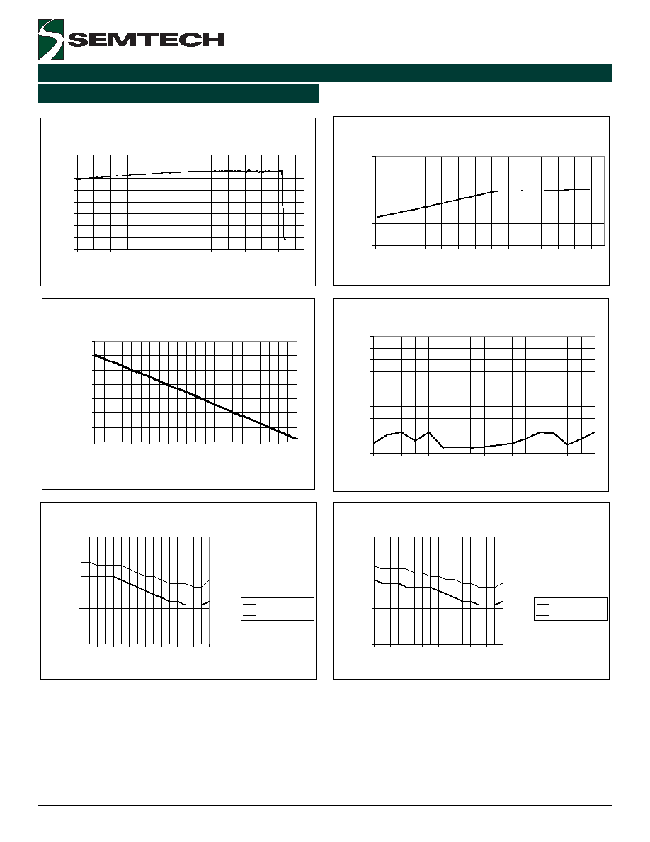
Typical Characteristics
Fast Charge Current vs IPRGM Resistance
0
200
400
600
800
1000
1200
1400
1.2 1.3 1.5 1.6 1.9 2.2 2.6 3.1 4.0 5.6 9.4 27.6
IPRGM Resistance (kohm )
Fast Charge Current (mA)
Output Voltage vsTemperature
4.18
4.19
4.2
4.21
-40 -20
0
20
40
60
80 100 120
Temperature (Degrees C)
Output Voltage (Volts)
ILOAD = 250mA
ILOAD = 500mA
Output Voltage vs Temperature
4.08
4.09
4.1
4.11
-40 -20
0
20
40
60
80 100 120
Temperature (Degrees C)
Output Voltage (Volts)
ILOAD = 250mA
ILOAD = 500mA
Charge Mode Bias Current vs Input Voltage
1
1.25
1.5
1.75
2
4.3
4.7
5.1
5.5
5.9
6.3
6.7
Input Voltage (Volts)
Bias Current (mA)
LDO Mode Bias Current vs Input Voltage
0
2
4
6
8
10
12
14
16
4.3 4.5 4.7 4.9 5.1 5.3 5.5 5.7 5.9 6.1 6.3 6.5 6.7 6.9
Input Voltage (Volts)
Bias Current (mA)
Vout Leakage Current vs Temperature
0
0.1
0.2
0.3
0.4
0.5
0.6
0.7
0.8
0.9
1
-40
-20
0
20
40
60
80
100
120
Temperature (Degrees C)
Leakage Current (uA)
15
2002 Semtech Corp.
www.semtech.com
5+&
POWER MANAGEMENT
IPRGM Voltage vs Output Current
0
200
400
600
800
1000
1200
1400
1600
0
200
400
600
800 1000
Output Current (mA)
I
PRGM Voltage (m
V)
RPRGM = 1.87K
Dropout Voltage vs Output Current
50
150
250
350
450
550
650
10
210
410
610
810
1010
Output Current (mA)
D
ropout Voltage (m
V)
Typical Characteristics
Battery Charge Profile
1.5
2
2.5
3
3.5
4
4.5
0:00
0:10
0:20
0:30
0:40
0:50
1:00
1:10
1:20
1:30
1:40
1:50
Charge Time
Charge Voltage (Volts)
0
0.1
0.2
0.3
0.4
0.5
0.6
0.7
0.8
0.9
1
Charge Current (Amps)
Vout
Iout
16
2002 Semtech Corp.
www.semtech.com
5+&
POWER MANAGEMENT
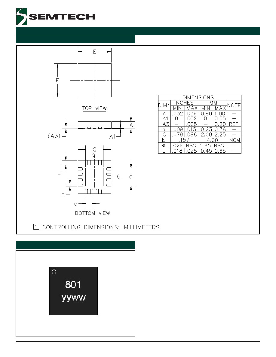
Outline Drawing - MLP (16 pin)
Marking Information
yy = two-digit year of manufacture
ww = two-digit week of manufacture
Top Mark
17
2002 Semtech Corp.
www.semtech.com
5+&
POWER MANAGEMENT
Semtech Corporation
Power Management Products Division
652 Mitchell Rd., Newbury Park, CA 91320
Phone: (805)498-2111 FAX (805)498-3804
Contact Information
Z
Z
;
:
-
+
+
5
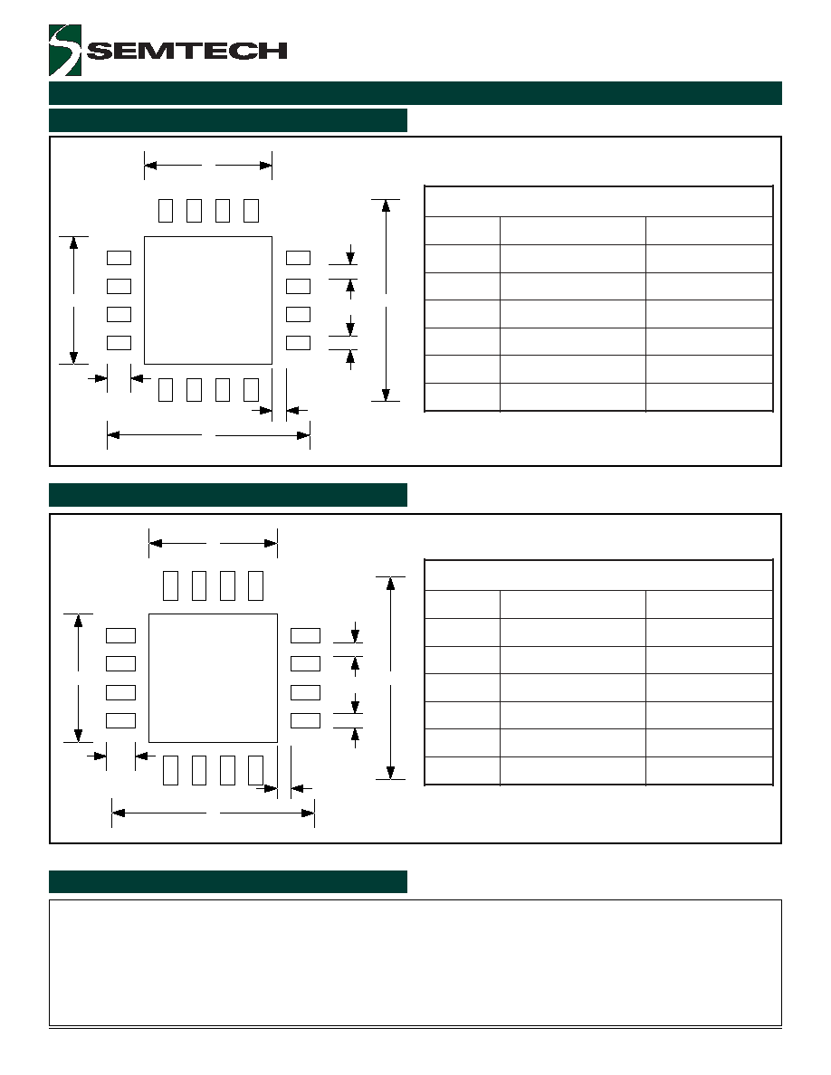
Land Pattern MLP-16 pin (Extended Lead)
Land Pattern MLP-16 pin (Standard Lead)
Z
Z
;
:
-
+
+
5
S
N
O
I
S
N
E
M
I
D
M
I
D
S
E
H
C
N
I
M
M
C
0
8
8
0
.
0
2
5
3
2
.
2
E
0
9
0
0
.
0
6
8
2
2
.
0
S
5
8
0
0
.
0
9
5
1
2
.
0
X
0
7
1
0
.
0
8
1
3
4
.
0
Y
0
9
2
0
.
0
6
6
3
7
.
0
Z
0
2
6
1
.
0
8
4
1
1
.
4
S
N
O
I
S
N
E
M
I
D
M
I
D
S
E
H
C
N
I
M
M
C
0
8
8
0
.
0
2
5
3
2
.
2
E
0
9
0
0
.
0
6
8
2
2
.
0
S
5
8
0
0
.
0
9
5
1
2
.
0
X
0
7
1
0
.
0
8
1
3
4
.
0
Y
0
9
3
0
.
0
6
0
9
9
.
0
Z
0
2
8
1
.
0
8
2
2
6
.
4