1
www.semtech.com
SC804A
Fully Integrated 4.4V Lithium-Ion
Battery Charger System with Timer
PRELIMINARY
POWER MANAGEMENT
October 4, 2005
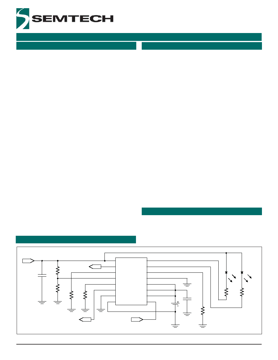
Typical Application Circuit
Applications
Description
Features
The SC804A is a fully integrated full-feature, single cell
constant-current/constant-voltage (CC/CV) 4.4V Lithium-
Ion battery charger. With an integrated timer and
complete charge control algorithm, the SC804A is ideal for
stand-alone charger applications. The SC804A contains
programmable pre-charge, fast-charge and termination
current settings. The SC804A can be programmed to
terminate charging based on the output current or the
time-out of the programmable timer. The fast charge
current is typically set with an external resistor, but it can
also be adjusted by applying an analog voltage to the AFC
pin. This feature allows use of a microcontroller to set
charging current via a DAC output.
The SC804A's 14V input voltage range eliminates the
need for additional protection circuitry required by other
5V chargers to protect against faulty adapters. The
SC804A also incorporates an under-voltage lockout falling
threshold of 3V so that charging will continue if the input
supply goes into a current-limited mode.
Reference ground and battery sense inputs are provided
to eliminate voltage drops during charging due to high
charging currents.
The output voltage to the battery is controlled to within
1% of the programmed voltage. The SC804A can also
function as a general purpose current source or as a
current source for charging nickel-cadmium (NiCd) and
nickel-metal-hydride (NiMH) batteries.
Typical Application Circuit
Fully integrated charger with FET pass transistor,
reverse-blocking diode, sense resistor, timer, and
thermal protection
Battery voltage controlled to 1% accuracy
Programmable precharge, fastcharge & termination
current over wide range, with analog current control
reference input for design fl exibility
Up to 1.5A continuous charge current
Input voltage range from 3V to 14V
Soft-start reduces start-of-charge adapter
load transients
NTC thermistor sense input and adjustable cold
temperature threshold
Adjustable 2 - 6 hour programmable charge timer
0.1A battery drain current in shutdown and monitor
modes
Small 4mm x 4mm 16 lead MLPQ package
Over-current protection in all modes
Over-voltage protection
Remote Kelvin sensing at the battery terminals
Status indicators for charger-present, charger-active,
over-voltage fault, and error notifi cation
Cellular phones
PDAs
Handheld meters
Charging stations
Handheld computers
Digital cameras
Programmable current
source
VCC
14
OVPB
13
3
IPRGM
7
NTC
CPB
CHRGB
RTIM
CTO
11
10
12
2
ITERM
4
FLTB
8
6
GND
5
RGND
BSEN
VOUT
VOUT
AFC
1
16
15
9
SC804A
C1
2.2
F
R3
Battery
Red
Green
Charger VIN
RT
NTC
R1
R2
DAC ISET
C2
2.2
F
R4
R5
R6
ERROR
OV_FLT
2
© 2005 Semtech Corp.
www.semtech.com
SC804A
PRELIMINARY
POWER MANAGEMENT
DRAFT
Electrical Characteristics
Unless otherwise noted: VCC = 4.75V - 5.25V. Typical values are at T
A
= 25∞C Min and Max are for -40∞C < T
A
< +85∞C unless noted.
Parameter
Symbol
Conditions
Min
Typ
Max
Units
Operating Voltage
VCC
OP
4.28
5.0
6.22
(1)
V
VCC UVLO Rising Threshold
VT
UVLOR
Charging begins when
threshold is exceeded
3.88
4.08
4.28
V
VCC UVLO Falling Threshold
VT
UVLOF
Charging continues until
threshold is reached
2.86
3.06
3.26
V
VCC OVP
Rising Threshold
VT
OVPR
6.63
6.94
7.40
V
VCC OVP
Falling Threshold
VT
OVPF
6.22
6.63
7.00
V
VCC OVP Hysteresis
VT
OVPH
200
350
600
mV
Operating Current
ICC
DIS
Shutdown Mode - CHRGB, CPB,
OVPB, FLTB off NTC = 0V
1.9
mA
ICC
CHG
Charging Mode - CHRGB, CPB,
OVPB, FLTB off NTC = 2.5V
2.0
Exceeding the specifi cations below may result in permanent damage to the device or device malfunction. Operation outside of the parameters specifi ed in the
Electrical Characteristics section is not implied.
Parameter
Symbol
Maximum
Units
VCC, CTO, NTC to GND
-0.3 to 14.0
V
VOUT, BSEN, RTIM, AFC, IPRGM, CPB, CHRGB, OVPB,
ITERM, FLTB, to GND
-0.3 to +6.0
V
RGND to GND
-0.3 to 0.3
V
VOUT Output Current
I
VOUT
1.5
A
Power Dissipation MLP (Derate 20mW/∞C above 85∞C)
Pd
2
W
Thermal Impedance, Junction to Ambient
(1)
JA
48
∞C/W
Junction Temperature
T
J
150
∞C
Operating Ambient Temperature Range
T
A
-40 to +85
∞C
IR Refl ow Temperature
T
LEAD
260
∞C
Storage Temperature Range
T
STG
-65 to 150
∞C
VOUT short to GND
Continuous
ESD Protection Level
(2)
V
ESD
2
kV
Absolute Maximum Ratings
Notes:
1) Calculated from package in still air, mounted to 3" x 4.5", 4 layer FR4 PCB with thermal vias under the exposed pad per JESD51 standards.
2) Tested according to JEDEC standard JESD22-A11 4-B.
3
© 2005 Semtech Corp.
www.semtech.com
SC804A
POWER MANAGEMENT
Electrical Characteristics (Cont.)
Parameter
Symbol
Conditions
Min
Typ
Max
Units
Battery Leakage Current
(VOUT and BSEN)
ILEAK
BAT
VCC = 0V,
VOUT = BSEN = 4.5V
0.1
2
A
Regulated Constant
Voltage
V
CV
0∞C T
J
125∞C
4.314
4.357
4.40
V
RGND Output Accuracy
VOUT = VOUT
NOM
+ RGND
V
RGND
RGND - GND = 30mV
22
30
38
mV
RGND Current
I
RGND
RGND = 0V
35
A
Battery Pre-Charge Current
I
PREQ
R
ITERM
= 499, 0∞C T
J
125∞C
270
300
330
mA
Battery Termination
Current
I
TERM
R
ITERM
= 499, 0∞C T
J
125∞C
270
300
330
mA
Battery Fast-Charge
Current
I
FAST
R
PRGM
= 1.87k, VOUT = 3.8V
0∞C T
J
125∞C
753
815
878
mA
AFC DAC
Fast-Charge Current
I
DACADJ
R
PRGM
= 1.87k, V(AFC) = 0.75V
0∞C T
J
125∞C
364
405
447
mA
AFC Enable/Disable
Threshold
VT
AFC
VCC - V
AFC
> VT
AFC
disables
Analog Fast Charge
1
V
ITERM Regulated
Voltage
V
ITERM
1.45
1.557
1.66
V
IPROG Regulated
Voltage
V
IPRGM
1.45
1.557
1.66
V
V
BAT
Precharge
Threshold
VT
PreQ
0∞C T
J
125∞C
2.9
3.01
3.11
V
V
BAT
Recharge
Threshold
VT
ReQ
V
CV
- V
BSEN
, 0∞C T
A
85∞C
60
100
140
mV
Over-Temperature
Shutdown
T
OT
Hysteresis = 10∞C
150
∞C
4
© 2005 Semtech Corp.
www.semtech.com
SC804A
PRELIMINARY
POWER MANAGEMENT
DRAFT
Electrical Characteristics (Cont.)
Parameter
Symbol
Conditions
Min
Typ
Max
Units
NTC Thresholds
VT
NTCDIS
SC804A Disabled
0.3
0.6
0.8
V
VT
NTCH
NTC Hot V
TH
Applies to falling threshold
4.3V VCC 6.5V
at VCC = 5V
29
1.45
30
1.50
31
1.55
% of
VCC
V
VT
NTCC
NTC Cold V
TH
, V
CTO
= 0V
Applies to rising threshold
4.3V VCC 6.5V
at VCC = 5V
73.4
3.67
74.4
3.72
75.4
3.77
% of
VCC
V
VT
NTCHYS
NTC Hot & Cold VT
NTCx
hysteresis
(VT
NTCx
Rising - VT
NTCx
Falling)
Applies to internal NTC thresholds
50
mV
V
CTO
CTO Voltage (Adjustable NTC
Cold Rising Threshold) Setting
Range
(2)
, -40∞C T
A
25∞C
(NTC
Cold Rising Threshold is VT
NTCC
when CTO tied to GND)
50
90
% of
VCC
Threshold Error
(3)
,
-40∞C T
A
25∞C
-70
70
mV
VT
CTOHYS
Internal hysteresis on CTO
(V
CTO
Rising - V
CTO
Falling)
Applies to externally set
NTC cold threshold
50
mV
Adjust Mode BSEN Voltage
V
BSEN-ADJ
3.5V VOUT VCC - 150mV
0∞C T
J
125∞C
3.189
3.217
3.253
V
Adjust Mode Enable Voltage,
VOUT-BSEN
V
ADJEN
3.5V VOUT VCC - 150mV
400
mV
Adjust Mode Disable
Voltage, VOUT-BSEN
V
ADJDIS
3.5V VOUT VCC - 150mV
150
mV
External RTIM
Regulation Voltage
V
RTIM
R
RTIM
= 37.4k
1.450
1.557
1.660
V
Timer Disable
Threshold
VT
TIMER
V
RTIM
VT
TIMER
disables internal timer
0.65
0.85
V
Internal Timer Select
VT
INTTS
VCC-V
RTIM
> VT
INTTS
selects internal timer
1.1
V
5
© 2005 Semtech Corp.
www.semtech.com
SC804A
POWER MANAGEMENT
Electrical Characteristics (Cont.)
Parameter
Symbol
Conditions
Min
Typ
Max
Units
Pre-Charge Fault
Time-out
T
PreQF
R
RTIM
= 37.4k
RTIM pulled to VCC
-20%
-35%
51
44
+20%
+35%
min
Complete Charge
Time-out
T
QCOMP
R
RTIM
= 37.4k
RTIM pulled to VCC
-20%
-35%
3.37
2.89
+20%
+35%
hr
CHRGB On
V
CHRGB
Load = 5mA
0.5
1
V
CHRGB Off
I
CHRGB
Leakage Current, V = 5V
1
A
CPB On
V
CPB
Load = 5mA
0.5
1
V
CPB Off
I
CPB
Leakage Current, V = 5V
1
A
OVPB On
V
OVPB
Load = 5mA
0.5
1
V
OVPB Off
I
OVPB
Leakage Current, V = 5V
1
A
FLTB On
V
FLTB
Load = 5mA
0.5
1
V
FLTB Off
I
FLTB
Leakage Current, V = 5V
1
A
Notes:
1)
VCC_OP Max is the "Maximum Vsupply" as defi ned in EIA/JEDEC Standard No. 78, paragraph 2.11.
2) The absolute voltage on CTO must not exceed 6.0V to ensure normal operation.
3) The threshold error is tested at V
CTO
min and max only.
6
© 2005 Semtech Corp.
www.semtech.com
SC804A
PRELIMINARY
POWER MANAGEMENT
DRAFT
DEVICE
PACKAGE
SC804AMLTRT
(1)
MLPQ -16
(2)
SC804EVB
Evaluation Board
(2)
Pin Descriptions
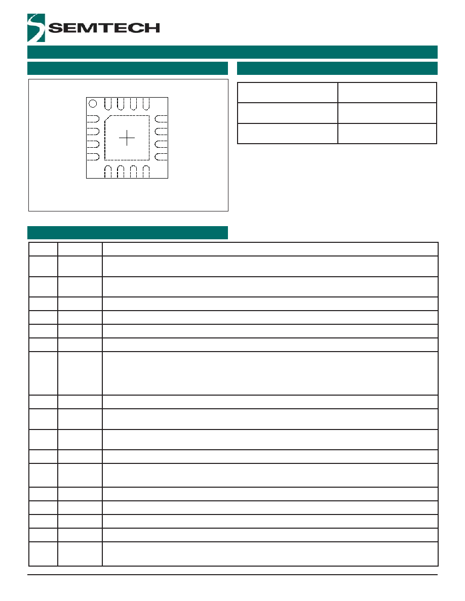
Pin Confi guration
Notes:
1) Available in tape and reel packaging only. A reel contains 3000
devices.
2) Available in lead-free packaging only. This product is fully WEEE
and RoHS compliant.
Pin #
Pin Name
Pin Function
1
BSEN
Battery voltage sense. Connect to battery positive terminal for Kelvin voltage sensing, VOUT otherwise.
Do not leave open.
2
CTO
Cold Temperature Offset. Adjustable NTC input high voltage (cold temperature) threshold. When the pin
is connected to GND the NTC high voltage threshold defaults to VT
NTCC
◊V
VCC
.
3
IPRGM
Charger current program pin for fast-charge mode. Requires a resistor to GND to program fast-charge current.
4
ITERM
Charger termination current program pin. Requires a resistor to GND to program pre-charge and termination current.
5
RGND
Reference ground. Connect to battery's negative terminal for Kelvin voltage sensing, GND otherwise. Do not leave open.
6
GND
Ground.
7
NTC
Input for battery NTC thermistor network. Voltage between VT
NTCH
◊V
VCC
, normally the hot threshold, and the CTO voltage
(VT
NTCC
◊V
VCC
if CTO is tied to GND), normally the cold threshold, enables charging. Voltages outside this range suspend
charging and drive FLTB pin active (low). Voltage below VT
NTCDIS
(nominally 0.6V) disables the SC804A and resets the
charge timer (with FLTB pin inactive).
8
FLTB
Open drain fault indicator. Active low when a fault condition occurs.
9
AFC
Analog Fast Charge input. Connect to a DAC for analog control of fast charge current level, connect to VCC
to disable this feature. Do not leave open.
10
CHRGB
Open drain charge status indicator. Active low when the charger is on and the output current exceeds the
termination current setting, high impedance when I
VOUT
< ITERM.
11
CPB
Open drain charger-present indicator. Active low when VCC exceeds UVLO.
12
RTIM
Programmable timer input pin. Connect to VCC to select the default time-out of 3 hrs., connect to GND
to disable timer, or connect an external resistor to GND to program the time-out period.
13
OVPB
Open drain over-voltage indicator. Active low when an input over-voltage fault occurs.
14
VCC
Input supply pin. Connect to adapter power.
15
VOUT
Charger output. Connect to battery.
16
VOUT
Charger output. Connect to battery.
T
THERMAL
PAD
Thermal-conduction pad on bottom of the package. Solder directly to the ground plane with multiple
thermal vias to all other ground planes.
Ordering Information
TOP VIEW
1
2
3
4
12
11
10
9
16
15
14
13
5
6
7
8
MLPQ16: 4X4 16 LEAD
T
VOU
T
VC
C
VOU
T
OVP
B
RG
ND
GN
D
NT
C
FL
TB
AFC
CHRGB
CPB
RTIM
BSEN
CTO
IPRGM
ITERM
7
© 2005 Semtech Corp.
www.semtech.com
SC804A
POWER MANAGEMENT
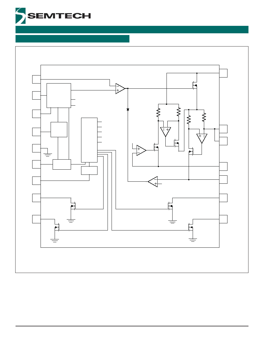
Block Diagram
Figure 1 - SC804A Functional Block Diagram
Reference
Voltages
5
12
7
10
11
13
6
15
3
4
VOUT
IPRGM
ITERM
GND
NTC
CHRGB
CPB
RGND
V
CV
(V
BSEN-ADJ
in Adj. Mode)
Fast-Charge Ref
NTC
Interface
Pre - Charge Ref
RTIM
Control
Timer
Pre-Charge On
Fast-Charge On
Over-Temp
Under-Voltage
Over-Voltage
14 VCC
16
VOUT
1
BSEN
9
AFC
2
CTO
8
FLTB
OVPB
VT
NTCH
VT
NTCC
V
IPRGM
V
ITERM
Cold
Threshold
Offset

8
© 2005 Semtech Corp.
www.semtech.com
SC804A
PRELIMINARY
POWER MANAGEMENT
DRAFT
Fast-Charge Mode (CC)
The fast-charge CC (Constant Current) mode is active when
the battery voltage is above VT
PreQ
and less than V
CV
.
The
fast-charge current can be set to a maximum of 1.5A and
is selected by the program resistor on the IPRGM pin. The
voltage on this pin will represent the current through the
battery, enabling a microprocessor via an analog-to-digital
converter (ADC) to monitor battery current by sensing the
voltage on the IPRGM pin. The equation to set the fast-
charge current is given by:
The superior fast-charge current accuracy of the SC804A
is obtained by use of a patented* polarity-switched
(i.e., chopped) current sense amplifi er to nullify current
measurement offset errors.
Compliance with the absolute maximum output current
I
VOUTMAX
, allowing for current regulation tolerance, requires
that R
IPRGM
be no smaller than 1.05k
nominal. R
IPRGM
can
be as large as 15k
, for a nominal FCI as small as 100
mA. Note that for a given program resistor the current
through the battery in CV mode can be determined by
replacing V
IPRGM_Typ
with the actual voltage on the IPRGM
pin in the above equation. The CC current can also be
modifi ed by applying an analog voltage to the AFC pin as
described below.
Analog Fast Charge (AFC Pin)
Many applications require more than one current setting
for fast-charge. This behavior is obtained in the SC804A
using the AFC function. When the AFC pin is connected
to VCC the device behaves as described in the previous
section. When the AFC pin is driven by an analog voltage
between 0V and (V
VCC
-1.0)V, the SC804A automatically
uses this pin voltage to set the maximum fast-charge
current according to the following equation:
This adjustment to the fast charge current is obtained
by replacing the fi xed V
IPRGM
reference voltage with the
General Operation
The SC804A can be confi gured independently with respect
to fast-charge and termination current, output voltage,
and timing, depending on the application. A typical
charging cycle is described below. Details on alternative
applications and output programmability are covered in
the individual sections.
The charging cycle begins when the power adapter is
connected to the device. The SC804A performs glitch
fi ltering on the VCC input and initiates a charge cycle
when V
VCC
is greater than the under-voltage lockout (UVLO)
rising threshold voltage. If the battery voltage is less than
the pre-charge threshold level, the SC804A will output the
pre-charge current. Once the pre-charge threshold voltage
is exceeded, the SC804A enters fast-charge constant
current (CC) mode. When the battery voltage reaches its
fi nal value, the charger enters the constant voltage (CV)
mode. In this mode the output current decreases as the
battery continues to charge until the termination current
level is reached. The CHRGB output turns off when IOUT
drops below the termination current. If the charge timer
is active, the SC804A continues to hold the battery in
CV charge mode until the timer expires. When the timer
expires the charger enters the monitor mode where the
output remains off until the voltage at VOUT drops by
VT
ReQ
. At this point a new charge cycle is initiated.
Pre-Charge Mode
Pre-charge mode is automatically enabled whenever
the battery voltage is below the pre-charge threshold
voltage, VT
PreQ
. It is used to limit the power dissipation and
precondition the battery for fast charging. The pre-charge
current value is determined by the resistor on the ITERM
pin. The pre-charge current is programmable from 50mA
to 350mA. The equation to select the pre-charge current
is given by:
where V
ITERM_Typ
designates the typical value of V
ITERM
. When
the timer is enabled there is also a maximum allowed pre-
charge duration. If the pre-charge time exceeds 25% of
the total charge cycle the charger will turn off due to a
pre-charge fault. This fault is cleared when VCC is toggled
or the output voltage rises above VT
PreQ
.
Applications Information
PCI =
V
ITERM_Typ
◊ 100
R
ITERM
FCI =
V
AFC
◊ 1000
R
IPRGM
*US Patent 6,836,095.
◊ 1000
FCI =
R
IPRGM
V
IPRGM_Typ
9
© 2005 Semtech Corp.
www.semtech.com
SC804A
POWER MANAGEMENT
internal timer, and to GND to disable the timer.
Connecting a resistor between RTIM and GND will program
the total charge time according to the following equation:
R
RTIM
1
Charge time =
(
--------
)
◊
------
3.08
3600
With charge time expressed in hours. The timer is
programmable over the range of 2 to 6 hours. The internal
timer selection results in a charge time of 3 hours. The
SC804A will automatically turn off the output when the
charge timer times out.
NTC Interface
The NTC pin provides an interface to a battery pack
Negative Temperature Coeffi cient (NTC) thermistor. The
typical NTC network has a fi xed resistor from VCC to the
NTC pin, and the battery pack NTC thermistor connected
from the NTC pin to ground. In this confi guration, an
increasing battery temperature produces a decreasing
NTC pin voltage, and a decreasing battery temperature
produces an increasing NTC pin voltage.
This confi guration is shown in the typical application
schematic on page 1 of this datasheet. When the NTC
voltage from the divider is greater than the high (cold)
threshold or less than the low (hot) threshold, the SC804A
suspends the charge cycle by turning off the output, halting
(but not resetting) the charge timer, and indicating a fault
on the FLTB pin. Hysteresis is included for both high and
low NTC thresholds to avoid chatter at the NTC trip points.
When the NTC pin voltage returns to the valid range, the
SC804A automatically resumes the charge cycle. The
charge timer will time-out when the SC804A output on-
time exceeds the timer setting regardless of how long it
has been disabled due to the NTC temperature.
An input voltage between
VT
NTCH
◊V
VCC
and the CTO input
voltage V
CTO
(
VT
NTCC
◊V
VCC
if CTO is tied to GND) enables
charging. An input voltage outside this range suspends
charging and drives FLTB pin active (low). The internal
NTC thresholds of
VT
NTCH
and
VT
NTCC
were designed to
work with standard thermistors available from numerous
vendors.
NTC pin voltage below VT
NTCDIS
(nominally 0.6V) disables
the SC804A and resets the charge timer (with the FLTB
pin inactive). The NTC pin can be pulled down to ground
Applications Information (Cont.)
AFC voltage. (Note that AFC voltages above VIPRGM will
produce I
VOUT
exceeding that specifi ed in the Fast-Charge
Mode (CC) section.)
Termination Current
Once the battery voltage reaches V
CV
the SC804A will
transition from constant current mode to constant voltage
mode. The current through the battery will decrease while
the voltage remains constant as the battery becomes fully
charged. When the current falls below the programmed
termination current set by the termination resistor
connected to the ITERM pin, the SC804A will disable
CHRGB. If the timer is enabled the output will continue
to fl oat-charge in CV mode until the timer expires. If the
timer is disabled, the output will turn off as soon as the
termination current level is reached. The equation to set
the termination current is given by:
ITERM can be programmed to be as high as 300mA or as
low as 50mA, though accuracy is not guaranteed below
100mA. ITERM must be programmed to be less than FCI
for correct operation of the charge cycle.
Monitor Mode
When a charge cycle is complete, the SC804A output
turns off and the device enters monitor mode. If the
voltage of the battery falls below the recharge threshold
(V
CV
- V
ReQ
), the charger will clear the charge timer and
re-initiate a charge cycle. The maximum current drain of
the battery during monitor mode will be no more than 1
A
over temperature. The status of the charger output as a
function of the timer and IOUT is tabulated below.
Charge Timer
The timer on the SC804A has two functions: to protect
in the event of a faulty battery and to maximize charging
capacity. The RTIM pin is connected to VCC to select the
Timer
Iout
Output State
T < Timeout
N/A
On
T > Timeout
N/A
Off
Disabled
< Itermination
Off
V
ITERM_Typ
ITERM =
◊ 100
R
ITERM

10
© 2005 Semtech Corp.
www.semtech.com
SC804A
PRELIMINARY
POWER MANAGEMENT
DRAFT
or R3 = 2.333◊R
HOT
= 13.624k
exactly. The closest 1%
standard nominal value is R3 = 13.7k
.
Step 2:
Verify acceptable thermistor self heating.
In
general, lower values of RT provide more noise immunity
for the NTC voltage, but at the expense of bias current
from the input adapter and power dissipation in the NTC
network. The dissipation constant is the power rating of
the thermistor resulting in a 1
o
C self heating error. The
greatest self-heating occurs at low thermistor resistance
(at high temperature). Since temperature sensing
accuracy matters only at the charging temperature range
thresholds, self heating is assessed only at the worst case
high temperature threshold of +40
o
C.
For V
VCC
= 5V, the 40
o
C NTC network current I
NTC_HOT
=
V
VCC
/(R3 + R
HOT
) = 0.246mA. Power dissipation in the
thermistor at this temperature, P
HOT
= R
HOT
◊ (I
NTC_HOT
)
2
=
0.38mW, for self heating of approximately 0.13
o
C. The
actual high temperature threshold will thus be lower by
0.13
o
C. This self-heating error is usually acceptable. If
it is not, then a thermistor with a greater R
HOT
must be
chosen.
Step 3:
Determine the desired high (cold) threshold
.
Compute the NTC network resistor divider voltage, as a
function of V
VCC
, at the cold temperature threshold.
Step 4:
Confi gure CTO.
If NTC
COLD
is suffi ciently close
to the default cold threshold (
VT
NTCC
◊V
VCC
), then simply
connect CTO to ground, disabling the CTO function, to
complete the design. But in this example it is not, so the
voltage on CTO must be set to 0.6591◊V
VCC
. The simple
resistive voltage divider network of Figure 2 can be used
to obtain the desired CTO voltage.
or
Applications Information (Cont.)
by an external n-channel FET transistor or processor GPIO
to disable or reset the SC804A.
Note that the response of the SC804A to NTC pin voltage
above the high threshold and below the low threshold
is the same. Thus it is possible to confi gure the NTC
network with the battery pack thermistor between NTC
and VCC, and a fi xed resistor between NTC and ground.
This confi guration may be useful if it is desired to reset the
charge timer (and the CHRGB output) when the battery
pack is removed (so the fi xed resistor pulls the NTC pin to
ground) while VCC is present.
Cold Temperature Offset (CTO)
The voltage applied to the CTO pin sets the NTC high
voltage (normally the cold temperature threshold) for the
NTC input. The default NTC high threshold (
VT
NTCC
◊V
VCC
)
can be selected by connecting the CTO pin to ground. If
it is desired to change this threshold, the voltage on the
CTO pin can be set between 0.5◊V
VCC
and 0.9◊V
VCC
.
This feature is especially useful if a single PCB design
is needed to satisfy similar applications with different
requirements. The temperature range for normal charging
can be adjusted by adjusting resistor values on a divider
network without changing the NTC thermistor, which
is often enclosed in the battery pack. An example of a
typical application is shown in Figure 2.
NTC/CTO Design Example
The following example assumes the NTC network
confi guration of Figure 2, with a fi xed resistor R3 connected
between NTC and VCC, and a battery NTC thermistor
RT connected between NTC and ground. The battery
temperature range over which charging is permitted is
specifi ed to be 0
o
C through 40
o
C. The datasheet for the
selected NTC thermistor indicates that RT = 5.839k
at
40
o
C, at RT = 26.49k
at 0
o
C, with a dissipation constant
DC = 3mW. Designate R
HOT
= 5.839k
and R
COLD
=
26.49k
.
Step 1:
Select R3.
For the normal (NTC thermistor to
ground) confi guration, solve the NTC network voltage
divider for R3 to place the NTC voltage at 0.3◊VCC when
RT = R
HOT
.
0.3 ◊ VCC =
VCC ◊ R
HOT
R3 + R
HOT
NTC
COLD
=
VCC ◊ R
COLD
= 0.6591 ◊ VCC
R3 + R
COLD
V
CTO
= NTC
COLD
= 0.6591 ◊ VCC =
VCC ◊ R
CT2
R
CT1
+ R
CT2
R
CT1
=
1 0.6591
= 0.5172
R
CT2
0.6591

11
© 2005 Semtech Corp.
www.semtech.com
SC804A
POWER MANAGEMENT
Applications Information (Cont.)
The choice of R
CT1
and R
CT2
is somewhat arbitrary. The
simplest approach is to pick one and compute the other.
A good choice here is R
CT1
= 115k
, and R
CT2
= 221k
, as
these standard 1% tolerance values produce the closest
match to the desired voltage divider ratio. With these
resistor nominal values,
which is, nominally, only 0.2% below the target value of
0.6591◊V
VCC
. The CTO network will present a load of only
15A to a 5V charging adapter. The nominal impedance
presented to the CTO pin is R
CT1
|| R
CT2
= 75.6k
. Any
impedance on the order of 100k
(or less) is acceptable.
Remote Kelvin Sensing at the Battery
The BSEN pin provides the positive Kelvin sensing voltage
feedback to the CV amplifi er and should be connected as
close to the battery + terminal as possible. Likewise, the
RGND pin should be connected directly to the negative
terminal of the battery. This allows the designer great
fl exibility in PCB layout and achieves greater accuracy
by sensing the battery voltage directly at the battery
terminals. When laying out the PCB, the designer should
route the BSEN and RGND trace directly to the battery
connection terminals, rather than just to the VOUT and
GND pins on the device.
Dropout Voltage
Dropout voltage is the smallest achievable difference
voltage between VCC and VOUT under a particular
operating condition. Dropout voltage is encountered
during CC charging whenever the current limit of the
charging adapter is less than the SC804A FCI programmed
current. In this case, the adapter voltage (the SC804A
input voltage) will be pulled down to the battery voltage
(the SC804A output voltage) plus the dropout voltage.
Dropout voltage is the larger of two values: (1) the I-R
component, which is the output current multiplied by the
minimum VCC-to-VOUT path resistance (which is highly
temperature dependent), and (2) a regulated minimum
difference voltage, which is output voltage dependent
but is independent of the output current. The regulated
minimum dropout voltage results from the collapse of
internal voltage references as VOUT pulls VCC down to
near, or below, V
CV
, creating a reduced output regulation
voltage approximately 200mV below VCC. Thus VCC
cannot be pulled down below VOUT + 200mV. The dropout
voltage will be larger than 200mV whenever the minimum
path resistance multiplied by the output current exceeds
200mV, but it cannot be smaller than 200mV.
This greatest-of-two-limit dropout voltage behavior is
evident in the dropout voltage typical performance plot.
When operating in Adjust Mode (next section), the
regulated minimum dropout voltage depends on the
programmed VOUT regulation voltage, and dropout also
varies with the actual output voltage during CC charging.
See Figure 4 for an illustration of dropout voltage data.
Adjust Mode
The SC804A can be confi gured for an output voltage
other than V
CV
using Adjust (ADJ) Mode. In Adjust Mode
the output voltage is determined by an external resistor
divider from VOUT to BSEN. When BSEN is connected in
this fashion, V
VOUT
(during Constant Voltage (CV) charging)
will be controlled such that the voltage at the BSEN pin
(V
BSEN
) is the reference voltage V
BSEN-ADJ
.
The output voltage can be set to any voltage desired by
an appropriate choice of divider network resistors, within
the following limits. When the SC804A is programmed for
adjust mode, V
VOUT
is required to be 150mV less than V
VCC
,
and V
VOUT
is required to be 400mV greater than V
BSEN
.
V
VOUT
within 150mV of V
BSEN
guarantees normal mode
operation. This implies that, for BSEN used as a Kelvin
sense of battery voltage, the product of the fast charge
current and the charge path resistance from VOUT to the
Kelvin sense point should not exceed 150mV to ensure
normal mode operation.
The SC804A Adjust Mode schematic is shown in Figures
3a and 3b. Referring to these schematics, the equation
for setting the output voltage is:
The capacitor C3 across R8 in the feedback network
introduces zero-pole frequency compensation for stability.
Place the zero according to the following equation to
ensure stability:
V
CTO
=
VCC ◊ R
CT2
= 0.6577 ◊ VCC
R
CT1
+ R
CT2
R11
◊ C3 = 1
2 ◊ 100kHz
VOUT = V
BSEN-ADJ_TYP
x
(
1 +
R11
)
R12
12
© 2005 Semtech Corp.
www.semtech.com
SC804A
PRELIMINARY
POWER MANAGEMENT
DRAFT
VCC
14
OVP
13
3
IPRGM
7
NTC
CPB
CHRGB
RTIM
CTO
11
10
12
2
ITERM
4
FLTB
8
6
GND
5
RGND
BSEN
VOUT
VOUT
AFC
1
16
15
9
SC804A
C1
2.2
F
R3
Red
Green
Charger VIN
RT
NTC
R1
R2
C2
2.2
F
R4
R5
R6
ERROR
R
CT1
R
CT2
OV_FLT
VCC
14
OVP
13
3
IPRGM
7
NTC
CPB
CHRGB
RTIM
CTO
11
10
12
2
ITERM
4
FLTB
8
6
GND
5
RGND
BSEN
VOUT
VOUT
AFC
1
16
15
9
SC804A
C1
2.2
F
R3
Red
Green
Charger VIN
RT
NTC
R1
R2
C2
2.2
F
R4
R5
R6
ERROR
R11
R12
OV_FLT
C3
VCC
14
OVP
13
3
IPRGM
7
NTC
CPB
CHRGB
RTIM
CTO
11
10
12
2
ITERM
4
FLTB
8
6
GND
5
RGND
BSEN
VOUT
VOUT
AFC
1
16
15
9
SC804A
C1
2.2
F
R3
Red
Green
Charger VIN
RT
NTC
R1
R2
C2
2.2
F
R4
R5
R6
ERROR
R11
R12
OV_FLT
C3
Applications Information (Cont.)
Figure 2 - Application Circuit with AFC Disabled, and with NTC and CTO Resistor Networks
Figure 3a - Application Circuit for Adjust Mode
Figure 3b - Application Circuit for Adjust Mode, with Adapter-only Voltage Sensing
13
© 2005 Semtech Corp.
www.semtech.com
SC804A
POWER MANAGEMENT
The actual dropout voltage is the greater of the Minimum Dropout
Voltage at various programmed V
CV
and instantaneous VOUT
voltages (shown here, with several programmed V
CV
voltages
indicated in the fi gure by `o'), and the IR drop due to the product
of IOUT and R
DS-ON
(not shown here). Adjust mode operation is
ensured for any IOUT current at programmed V
CV
voltages up to
approximately 4.41V.
Applications Information (Cont.)
FLAG
ON
OFF
CPB
UVLO < VCC < OVP
Input out of range
CHRGB
IOUT > ITERM
IOUT < ITERM
OVPB
VCC > OVP
VCC < OVP
FLTB
VCC > OVP
VCC UVLO
NTC Temp Fault
Pre-Charge Time-out
(OT (Tj > 150∞C)
Normal Operation or
NTC Disable
NOTE: When using Adjust Mode to program a CV regulation
voltage greater than V
CV
, care must be taken when CC
charging with a charging adapter operating in current
limit. Adapter current-limited operation occurs when
the adapter current limit is less than the programmed
SC804A fast charge current, such that the adapter voltage
is pulled down to V
VOUT
plus the SC804A dropout voltage.
A low adapter current limit multiplied by the low minimum
path resistance of the main pass transistor and current
sense resistor (as low as 290m
total at extremely low
temperature) can result in a voltage drop from VCC to
VOUT of less than 150mV if the Adjust Mode CV regulation
voltage is programmed above V
CV
+ 50mV. If V
VCC
- V
VOUT
< 150mV, Adjust Mode may not operate correctly. Adjust
Mode will operate correctly whenever the programmed
VOUT CV voltage is less than V
CV
+ 50mV, regardless of the
adapter current limit, because the regulated minimum
dropout voltage is always greater than 150mV in this
case. It will also operate correctly with an adapter current
limit greater than 550 mA, regardless of the programmed
output voltage, because the I-R dropout voltage will
exceed 150mV at even the lowest specifi ed operating
temperature. Normal mode (that is, not
Adjust Mode) has
a regulated minimum dropout voltage of approximately
200mV, which is constant for any V
VOUT
, and so operates
correctly for any adapter current limit.
Overcurrent and Max Temperature Protection
Overcurrent protection is inherent in all modes of operation.
When the device is in charge mode the output is current-
limited to either the pre-charge current limit value or the
fast charge current limit value depending on the voltage
at the output. Max die temperature protection is also
included. This feature allows the SC804A to operate
with maximum power dissipation by disabling the output
current when the die temperature reaches the maximum
operating temperature. The result is that the SC804A will
operate as a pulse charger in extreme power dissipation
applications, delivering the maximum allowable output
current while regulating the internal die temperature to a
safe level.
Indicator Flags
There are four indicator outputs/LED drivers ont he
SC804A; CPB (Charger Present), CHRGB (Charge Active),
OVPB (Over Voltage Fault), and FLTB (Fault). These outputs
are all active-low; open drain NMOS drivers capable of
sinking up to 10mA. The following table defi nes each
indicator's output state.
The CPB output can be used as a VCC-present indicator.
Regardless of teh state of NTC, the CPB output refl ects
the VCC voltage. When V
CC
is between the UVLO and OVP
thresholds the CPB output is low. If V
CC
is outside these
limits, this output is high impedance.
The CHRGB output indicates the charging status. When
the output current is greater than ITERM, CHRGB is low.
CHRGB is high impedance when IOUT is less than ITERM.
The CHRGB output is latched during the charge cycle
when the output current is less than ITERM. This latch is
reset when the battery enters a recharge cycle, or if NTC
or VCC are toggled.
3.2
3.4
3.6
3.8
4
4.2
4.4
4.6
0.2
0.4
0.6
0.8
Output voltage, V
Minimum dropout voltage, V
Figure 4 - Adjust Mode Minimum Dropout Voltage
14
© 2005 Semtech Corp.
www.semtech.com
SC804A
PRELIMINARY
POWER MANAGEMENT
DRAFT
Charge Mode Timing Diagram
VCC
VOUT
IOUT
CPB
CHRGB
TIMER
FLTB
NTC
UVLO
VT
PreQ
Pre-Charge
Soft Start
Fast Charge
Termination
Current
Re-Charge
Threshold
CC Mode
CV Mode
On
On
On
On
On
On
On
Off
Off
Off
Off
Off
Fault
Hold
Figure 5 - Charge Mode Timing
The OVPB signal is an active-low output that signals when
the input voltage exceeds the OVP threshold. When the
voltage on VCC is less than the OVP threshold voltage
this output is high impedance.
The FLTB output is activated when the device experiences
a fault condition. This output can be used to notify the
system controller of a fault condition when connected to
an interrupt input, or it can be used like CPB and CHRGB
to drive an indicator LED. There are fi ve fault modes
signaled by FLTB: input over-voltage, input under-voltage,
NTC temperature out of range, max die temperature (OT),
and pre-charge timeout. When any of these conditions
occurs the FLTB output goes low; otherwise it remains
high impedance.
Capacitor Selection
Low cost, low ESR ceramic capacitors such as the X5R and
X7R dielectric material types are recommended for use with
the SC804A. The output capacitance range is 1F to 4.7F.
The input capacitor is typically between 0.1F to 2.2F, but
larger values will not degrade performance
15
© 2005 Semtech Corp.
www.semtech.com
SC804A
POWER MANAGEMENT
State Diagram
Over-Voltage, Under-Voltage or
Over-Temperature will force the
SC804A into Shutdown Mode
from any state.
Soft Start CC Mode
Yes
I
OUT
= I
FAST
Yes
I
OUT
< I
TERM
V
OUT
< V
CV
- V
ReQ
low temp > NTC Temp
> high temp
Yes
Yes
Yes
Yes
Start Timer
Start CV Mode
Timer
Enabled?
CC = Constant Current
CV = Constant Voltage
Yes
Yes
OVP > VCC > UVLO
En = Hi
Soft Start Vout
CHRGB Low
Timer
Enabled?
Start Pre- Charge
I
OUT
= I
PREQ
Time > T
MAX
/4
Pre- Charge
Timeout Fault
FLTB goes low.
Cleared by
VBAT > VT
PreQ
or Re- cycle VCC
Yes
V
OUT
= V
CV
CHRGB High Z
Monitor Mode
V
OUT
off
Time > T
MAX
Float Charge Mode
V
OUT
= V
CV
NTC out of Range Fault
FLTB goes active low
Timer is frozen
Charge resumes when NTC
Temperature is valid
V
OUT
> VT
PreQ
Shutdown Mode:
V
OUT
& I
OUT
off,
CHRGB High Z,
CPB Low.
16
© 2005 Semtech Corp.
www.semtech.com
SC804A
PRELIMINARY
POWER MANAGEMENT
DRAFT
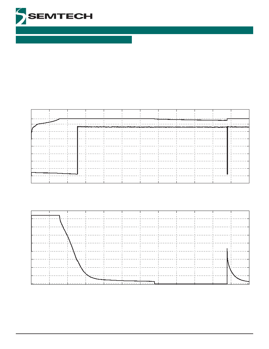
Typical Charge Cycle
Typical Charge Cycle
Evaluation Board confi gured for internal timer, 1.5V on IPRGM = 843mA, 1.5V on ITERM = 300mA, VCC = 5.0V, Li-Ion
battery capacity = 850mAh. A 237 load resistor (18mA at a battery voltage of 4.36V) was applied to the battery fol-
lowing completion of precharge, to slowly discharge the battery following charge timer timeout to illustrate a recharge
cycle. The alphabetic markers indicate the following: (a) precharge; (b) fast charge, or Constant Current (CC) charg-
ing; (c) Constant Voltage (CV) charging; (d) termination; (e) CV ("fl oat") charging until charge timer timeout; (f) charge
timer timeout; (g) discharge of the battery due to 18mA load; (h) recharge cycle initiated when battery voltage drops
below the recharge threshold.
0
30
60
90
120
150
180
210
240
270
300
330
360
0
0.5
1
1.5
2
2.5
3
3.5
4
4.36
5
0
30
60
90
120
150
180
210
240
270
300
330
360
0
100
200
300
400
500
600
700
800
900
Time (minutes)
I
VOUT
mA
V
BATTERY
,
V
CHRGB
,
(V)
Time (minutes)
b
a
c
d
e
f
g
h
a
b
c
f
h
17
© 2005 Semtech Corp.
www.semtech.com
SC804A
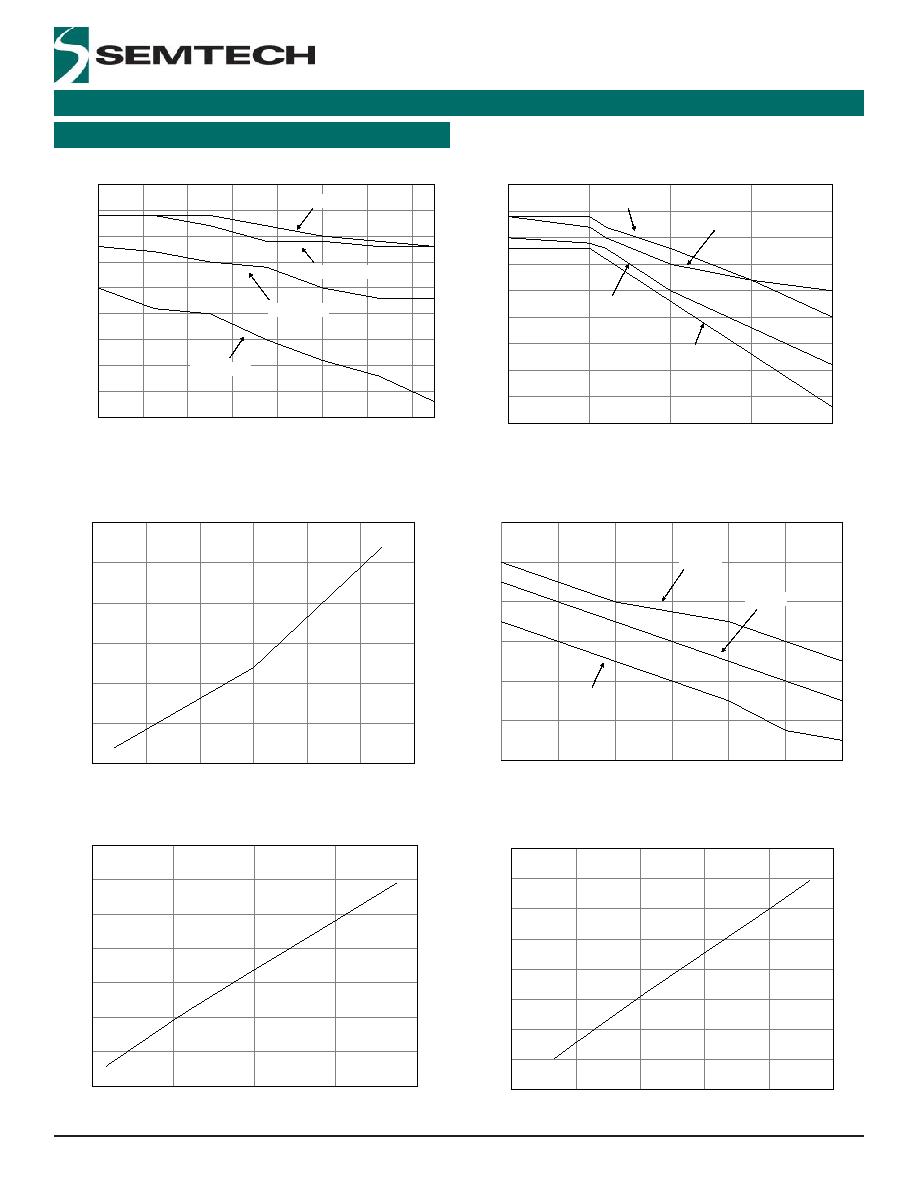
POWER MANAGEMENT
VOUT V
CV
Line Regulation vs. Load, T = +25∞C
VOUT V
CV
Load Regulation vs. Line, T = +25∞C
VOUT V
CV
Regulation vs. Temperature,
VCC = 5.0V, IOUT = 800mA
IOUT Line Regulation vs. Temperature,
RPRGM = 1.87k
IOUT vs. IPRGM Resistance, T = +25∞C
Precharge and Termination Current vs.
ITERM Resistance
Typical Characteristics
4.338
4.340
4.342
4.344
4.346
4.348
4.350
4.352
4.354
4.356
500
750
1000
1250
1500
IOUT (mA)
VOUT (V)
VCC = 5.0V
VCC = 5.5V
VCC = 6.0V
VCC = 6.5V
4.348
4.350
4.352
4.354
4.356
4.358
4.360
-50
-25
0
25
50
75
100
Ambient Temperature, ∞C
VOUT,V
816
820
824
828
832
836
840
5.00
5.25
5.50
5.75
6.00
6.25
6.50
VCC, V
IOUT, mA
T = +85∞C
T = +25∞C
T = -40∞C
4.338
4.340
4.342
4.344
4.346
4.348
4.350
4.352
4.354
4.356
5.00
5.20
5.40
5.60
5.80
6.00
6.20
6.40
VIN (V)
VOUT (V)
Iout = 500mA
Iout = 750mA
Iout = 1000mA
Iout = 1500mA
400
600
800
1000
1200
1400
1600
1800
0.3
0.5
0.7
0.9
1.1
1/Riprgm, 1/k
IOUT, mA
0.0
50.0
100.0
150.0
200.0
250.0
300.0
350.0
400.0
0
0.5
1
1.5
2
2.5
1/RIPRGM, 1/k
IOUT, mA
18
© 2005 Semtech Corp.
www.semtech.com
SC804A
PRELIMINARY
POWER MANAGEMENT
DRAFT
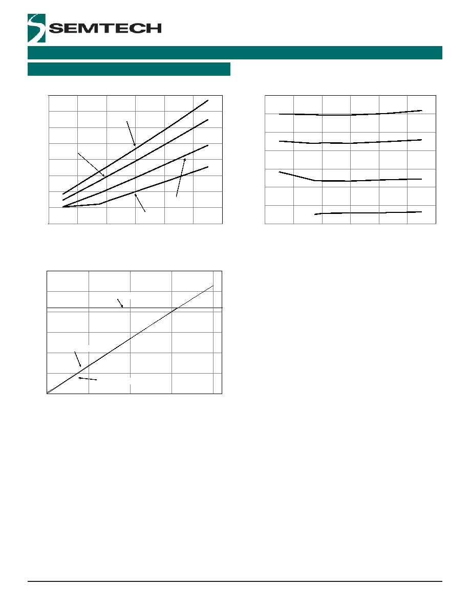
Typical Characteristics (Cont.)
Dropout Voltage vs. IOUT
Rds-on vs. IOUT
AFC Operation, RPRGM = 1.87k
Rds-on (
)
0.100
0.200
0.300
0.400
0.500
0.600
0.700
0.800
0.900
400
600
800
1000
1200
1400
1600
IOUT (mA)
Dropout (V)
T
J
= - 40∞C
T
J
= +25∞C
T
J
= +85∞C
T
J
= +125∞C
0.270
0.320
0.370
0.420
0.470
0.520
0.570
0.620
400
600
800
1000
1200
1400
1600
IOUT (mA)
T
J
= -40∞C
T
J
= +25∞C
T
J
= +85∞C
T
J
= +125∞C
0
200
400
600
800
1000
1200
0.000
0.500
1.000
1.500
2.000
V
AFC
, V
Iout, mA
AFC Pin Grounded
Actual AFC Response
Ideal AFC Response
19
© 2005 Semtech Corp.
www.semtech.com
SC804A
POWER MANAGEMENT
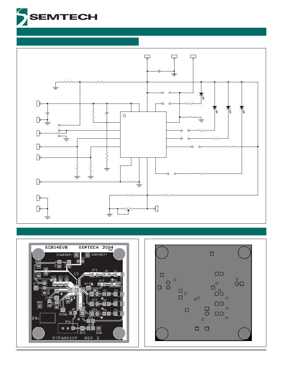
Evaluation Board Schematic
Evaluation Board Gerber Plot,Top/Bottom Views
1
2
D1
D1
1
2
R4
390
R4
390
1
2
D4
D4
1
2
R3
390
R3
390
1
GND
GND
1
RGND
RGND
1
2
R2
390
R2
390
1
2
R15
37.4k
R15
37.4k
1
CHARGER+
CHARGER+
BSEN
1
CTO
2
IPRGM
3
ITERM
4
RGND
5
GND
6
CPB
11
RTIM
12
OVPB
13
VC
C
14
VOUT
15
VOUT
16
CHRGB
10
NTC
7
AFC
9
FLTB
8
SC804A
U1
SC804A
U1
1
ITERM
ITERM
1
2
R1
390
R1
390
1
RTIM
RTIM
1
GND
GND
1
2
R8
<NM>
R8
<NM>
1
CTO
CTO
1
2
R7
10k
R7
10k
1
2
3
JP5
JP5
1
2
R11
0
R11
0
1
2
C3
<NM>
C3
<NM>
1
2
R14
0
R14
0
1
2
R9
<NM>
R9
<NM>
1
2
C2
2.2u
C2
2.2u
1
VOUT
VOUT
1
2
R13
100k
R13
100k
1
3
2
R16
POT_3296W-105
R16
POT_3296W-105
1
2
C1
2.2u
C1
2.2u
1
NTC
NTC
1
2
JP4
JP4
1
2
JP6
JP6
1
GND
GND
1
2
JP2
JP2
1
2
D3
D3
1
2
R12
<NM>
R12
<NM>
1
2
JP1
JP1
1
2
JP7
JP7
1
IPRGM
IPRGM
1
2
R10
<NM>
R10
<NM>
1
2
R6
1.87k
R6
1.87k
1
CHARGER-
CHARGER-
1
2
JP3
JP3
1
2
D2
D2
1
2
R5
499
R5
499
20
© 2005 Semtech Corp.
www.semtech.com
SC804A
PRELIMINARY
POWER MANAGEMENT
DRAFT
INDICATOR
(LASER MARK)
PIN 1
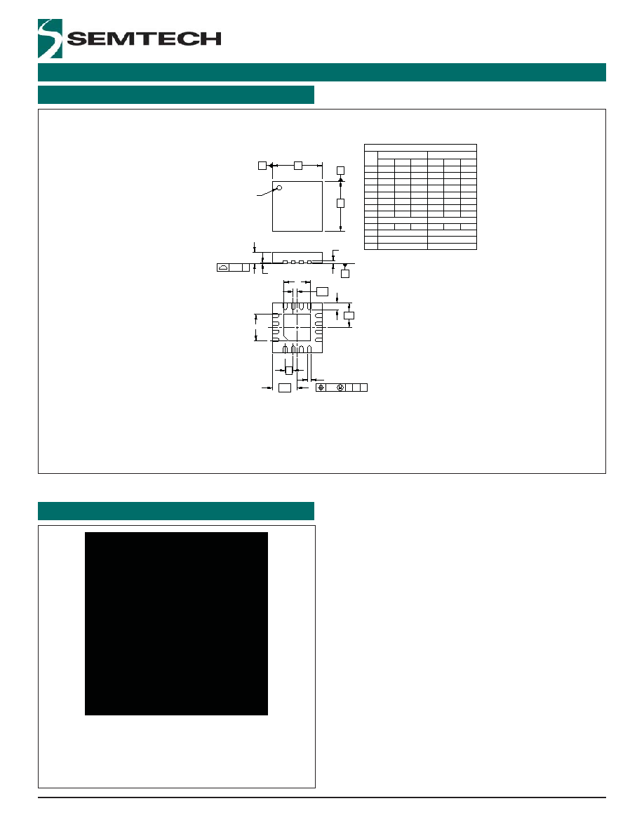
DIMENSIONS
NOM
INCHES
N
bbb
aaa
A2
A1
E1
D1
DIM
L
e
E
D
A
b
MIN
MAX
MILLIMETERS
MIN
MAX
NOM
.153
.157
.161
3.90
4.00
4.10
.153
.157
.161
3.90
4.00
4.10
E1
.003
.010
.079
16
.012
.085
-
.000
.031
(.008)
0.08
0.30
16
.014
.089
0.25
2.00
.040
-
.002
-
0.00
0.80
2.25
0.35
2.15
-
0.05
1.00
(0.20)
.004
0.10
2.00
2.15
2.25
0.65 BSC
.026 BSC
0.30
.012
.020
.016
0.40
0.50
.089
.085
.079
D/2
2
A
A1
1
LxN
bbb
C A B
A2
bxN
e
SEATING
PLANE
C
E/2
D1
N
e/2
aaa C
CONTROLLING DIMENSIONS ARE IN MILLIMETERS (ANGLES IN DEGREES).
COPLANARITY APPLIES TO THE EXPOSED PAD AS WELL AS THE TERMINALS.
1.
2.
NOTES:
A
D
E
B
-
-
-
-
Outline Drawing - MLPQ-16
Marking Information
804A
yyww
xxxxx
xxxx
yyww = Date Code (Example: 0552)
xxxxx xxxx = Semtech Lot Number
(Example: E9010 01-1)
21
© 2005 Semtech Corp.
www.semtech.com
SC804A
POWER MANAGEMENT
Land Pattern - MLPQ-16
Semtech Corporation
Power Management Products Division
200 Flynn Road, Camarillo, CA 93012
Phone: (805) 498-2111 FAX (805)498-3804
Contact Information
P
Y
K
C
Z
P
Y
X
G
K
H
.189
.026
.016
.033
.122
.091
.091
4.80
0.40
0.85
0.65
2.30
2.30
3.10
DIM
(3.95)
MILLIMETERS
DIMENSIONS
(.156)
INCHES
THIS LAND PATTERN IS FOR REFERENCE PURPOSES ONLY.
CONSULT YOUR MANUFACTURING GROUP TO ENSURE YOUR
COMPANY'S MANUFACTURING GUIDELINES ARE MET.
NOTES:
1.
2x G
H
2x (C)
2x Z
X