POWER MANAGEMENT
1
www.semtech.com
SC8863
150mA Ultra Low Dropout,
Low Noise Regulator
Revision 1, January 2001
The SC8863 is a low dropout linear regulator that
operates from a +2.5V to +6.0V input range and
delivers up to 150mA. A PMOS pass transistor allows
the low 110µA supply current to remain independent of
load, making these devices ideal for battery operated
portable equipment such as cellular phones, cordless
phones and personal digital assistants.
The SC8863 output voltage can be preset or adjusted
with an external resistor divider. Other features include
low power shutdown, short circuit protection, thermal
shutdown protection and reverse battery protection. The
SC8863 comes in the tiny 5 lead SOT-23 package.
u
Guaranteed 150mA output current
u
Works with ceramic capacitors
u
Fixed or adjustable output
u
Very small external components
u
Low 75µV
RMS
output noise
u
Very low supply current
u
Thermal overload protection
u
Reverse battery protection
u
Low power shutdown
u
Full industrial temperature range
u
Surface mount packaging (5 pin SOT-23)
u
Battery Powered Systems
u
Cellular Telephones
u
Cordless Telephones
u
Personal Digital Assistants
u
Portable Instrumentation
u
Modems
u
PCMCIA cards
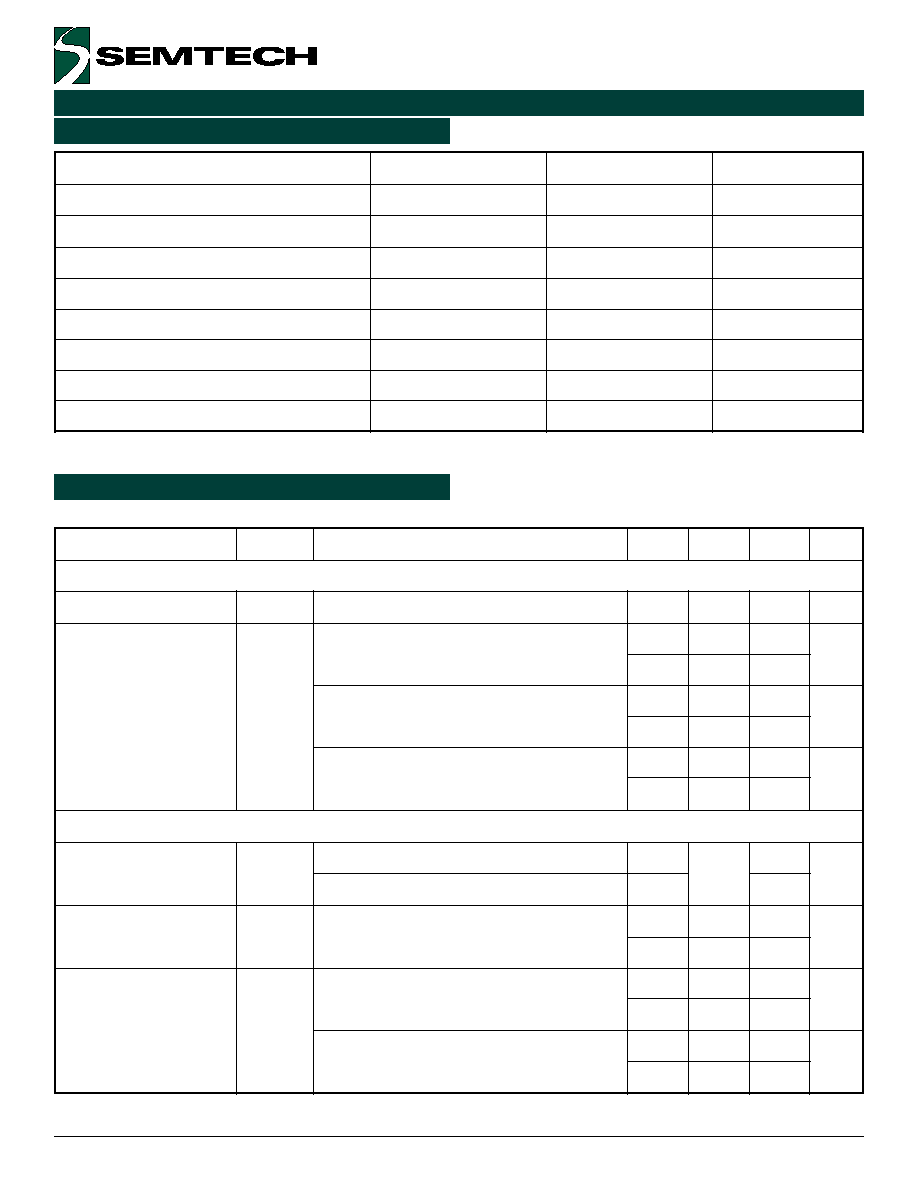
VIN > VOUT + VD(MAX)
VOUT @ IOUT up to 150mA
U1
SC8863
1
2
3
4
5
EN
GND
IN
OUT
SET
C1
1uF Ceramic
C2
1uF Ceramic
VOUT @ IOUT up to 150mA
VIN > VOUT + VD(MAX)
C2
2.2uF Ceramic
U1
SC8863
1
2
3
4
5
EN
GND
IN
OUT
SET
R1
R2
10k
C1
1uF Ceramic
+
∑
=
2
R
1
R
1
250
.
1
V
OUT
Description
Features
Applications
Typical Application Circuits
Internally Preset Output Voltage
Externally Preset Output Voltage
(1)
Note:
(1) Select R1 and R2 such that the current flowing through them is ≥ 10µA (i.e. R2 £ 120kW). A value of 10kW
is recommended for R2. Please see Component Selection - Externally Set Output on page 7.
3
„ 2001 Semtech Corp.
www.semtech.com
POWER MANAGEMENT
SC8863
r
e
t
e
m
a
r
a
P
l
o
b
m
y
S
s
n
o
it
i
d
n
o
C
t
s
e
T
n
i
M
p
y
T
x
a
M
s
ti
n
U
).
t
n
o
C
(
n
o
it
a
l
u
g
e
R
d
a
o
L
)
2
(
G
E
R
)
D
A
O
L
(
I
T
U
O
V
,
A
m
0
5
o
t
A
m
0
=
T
E
S
V
=
T
U
O
5
.
2
-
5
.
7
-
V
m
0
.
5
1
-
I
T
U
O
V
,
A
m
0
0
1
o
t
A
m
0
=
T
E
S
V
=
T
U
O
5
-
5
1
-
V
m
0
3
-
e
g
a
tl
o
V
t
u
o
p
o
r
D
)
3
()
2
(
V
D
I
T
U
O
A
m
1
=
1
.
1
V
m
I
T
U
O
A
m
0
5
=
5
5
0
9
V
m
0
2
1
I
T
U
O
A
m
0
0
1
=
0
1
1
0
8
1
V
m
0
4
2
ti
m
i
L
t
n
e
rr
u
C
I
M
I
L
0
5
1
0
4
2
0
5
3
A
m
e
s
i
o
N
e
g
a
tl
o
V
t
u
p
t
u
O
e
n
I
,
z
H
k
9
9
o
t
z
H
0
1
T
U
O
C
,
A
m
0
5
=
T
U
O
F
µ
1
=
0
9
V
µ
S
M
R
I
,
z
H
k
9
9
o
t
z
H
0
1
T
U
O
C
,
A
m
0
5
=
T
U
O
F
µ
0
0
1
=
5
7
n
o
it
c
e
j
e
R
y
l
p
p
u
S
r
e
w
o
P
o
it
a
R
R
R
S
P
f £
z
H
k
1
5
5
B
d
N
E
d
l
o
h
s
e
r
h
T
t
u
p
n
I
N
E
V
H
I
8
.
1
V
V
L
I
4
.
0
t
n
e
rr
u
C
s
a
i
B
t
u
p
n
I
N
E
)
4
(
I
N
E
V
N
E
V
=
N
I
0
0
0
1
A
n
0
0
2
T
E
S
d
l
o
h
s
e
r
h
T
t
c
e
l
e
S
/
e
s
n
e
S
V
H
T
0
2
5
5
0
8
V
m
e
g
a
tl
o
V
e
c
n
e
r
e
f
e
R
T
E
S
)
2
(
V
T
E
S
I
T
U
O
A
m
1
=
5
2
2
.
1
0
5
2
.
1
5
7
2
.
1
V
A
m
1
£ I
T
U
O
£
V
5
.
2
,
A
m
0
5
1
£ V
N
I
£
V
5
.
5
6
0
2
.
1
4
9
2
.
1
e
g
a
k
a
e
L
t
u
p
n
I
T
E
S
I
T
E
S
V
T
E
S
V
3
.
1
=
5
1
0
.
0
0
0
5
.
2
A
n
t
n
e
rr
u
C
)
4
(
0
0
0
.
5
n
o
it
c
e
t
o
r
P
e
r
u
t
a
r
e
p
m
e
T
r
e
v
O
l
e
v
e
L
p
ir
T
h
g
i
H
T
I
H
0
7
1
C
∞
s
i
s
e
r
e
t
s
y
H
T
T
S
Y
H
0
1
C
∞
Unless specified: V
IN
= 3.6V, V
SET
= GND, V
EN
= V
IN
, T
A
= 25∞C. Values in bold apply over full operating ambient temperature range.
Electrical Characteristics (Cont.)
(1)
Notes:
(1) This device is ESD sensitive. Use of standard ESD handling precautions is required.
(2) Low duty cycle pulse testing with Kelvin connections required.
(3) Defined as the input to output differential at which the output voltage drops 100mV below the value measured
at a differential of 2V.
(4) Guaranteed by design.
4
„ 2001 Semtech Corp.
www.semtech.com
POWER MANAGEMENT
SC8863
r
e
b
m
u
N
t
r
a
P
)
2
()
1
(
e
g
a
k
c
a
P
R
T
K
S
C
X
X
X
-
3
6
8
8
C
S
5
-
3
2
-
T
O
S
Notes:
(1) Where -XXX denotes voltage options. Available
voltages are: 2.50V (-250), 2.80V (-280), 3.00V (-300),
and 3.30 (-330)V.
(2) Only available in tape and reel packaging. A reel
contains 3000 devices.
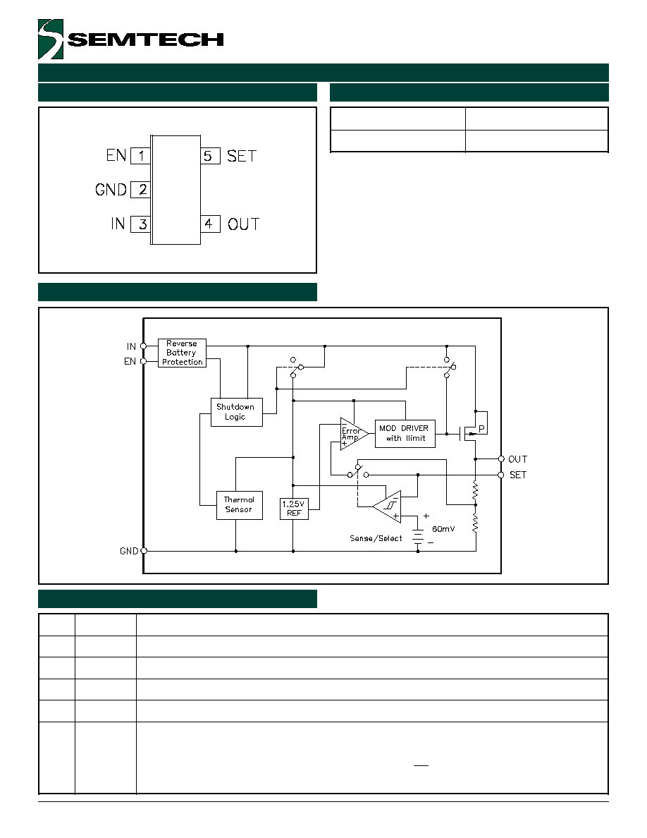
Top View
SOT-23-5
Pin Configuration
Ordering Information
n
i
P
e
m
a
N
n
i
P
n
o
it
c
n
u
F
n
i
P
1
N
E
V
o
t
t
c
e
n
n
o
C
.
n
i
p
e
l
b
a
n
e
h
g
i
h
e
v
it
c
A
N
I
.
d
e
s
u
g
n
i
e
b
t
o
n
fi
2
D
N
G
.
d
e
d
e
e
n
fi
g
n
i
k
n
i
s
t
a
e
h
r
o
f
d
e
s
u
e
b
n
a
C
.
n
i
p
d
n
u
o
r
G
3
N
I
.
n
i
p
t
u
p
n
I
4
T
U
O
.
A
m
0
5
1
o
t
p
u
g
n
i
c
r
u
o
s
,t
u
p
t
u
o
r
o
t
a
l
u
g
e
R
5
T
E
S
V
r
o
f
e
u
l
a
v
t
e
s
e
r
p
y
ll
a
n
r
e
t
n
i
e
h
t
n
i
s
tl
u
s
e
r
d
n
u
o
r
g
o
t
n
i
p
s
i
h
t
g
n
it
c
e
n
n
o
C
T
U
O
l
a
n
r
e
t
x
e
n
a
o
t
g
n
it
c
e
n
n
o
C
.
V
s
e
g
n
a
h
c
r
e
d
i
v
i
d
r
o
t
s
i
s
e
r
T
U
O
:
o
t
+
∑
=
2
R
1
R
1
250
.
1
V
OUT
Pin Descriptions
Block Diagram
5
„ 2001 Semtech Corp.
www.semtech.com
POWER MANAGEMENT
SC8863
2.74
2.75
2.76
2.77
2.78
2.79
2.80
2.81
2.82
2.83
2.84
2.85
2.86
0
25
50
75
100
125
150
I
OUT
(mA)
V
OUT
(V
)
V
IN
= 3.6V
T
J
= 25∞C
2.74
2.75
2.76
2.77
2.78
2.79
2.80
2.81
2.82
2.83
2.84
2.85
2.86
-50
-25
0
25
50
75
100
125
T
J
(∞C)
V
OUT
(V
)
IO = 1mA
IO = 50mA
IO = 100mA
IO = 150mA
V
IN
= 3.6V
1.225
1.230
1.235
1.240
1.245
1.250
1.255
1.260
1.265
1.270
1.275
0
25
50
75
100
125
150
I
OUT
(mA)
V
SET
(V
)
V
IN
= 3.6V
T
J
= 25∞C
1.210
1.220
1.230
1.240
1.250
1.260
1.270
1.280
1.290
-50
-25
0
25
50
75
100
125
T
J
(∞C)
V
SET
(V
)
IO = 1mA
IO = 50mA
IO = 100mA
IO = 150mA
V
IN
= 3.6V
0
25
50
75
100
125
150
175
200
225
250
0
25
50
75
100
125
150
I
OUT
(mA)
V
D
(m
V
)
-40∞C
25∞C
125∞C
SET = GND
0
2
4
6
8
10
12
-50
-25
0
25
50
75
100
125
T
J
(∞C)
REG
(L
INE)
(m
V
)
V
IN
= 2.5V to 5.5V
SET = OUT
I
OUT
= 1mA
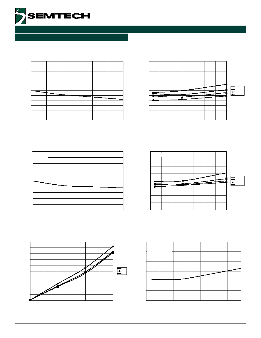
Dropout Voltage vs. Output Current
vs. Junction Temperature
Line Regulation vs.
Junction Temperature
Output Voltage vs.
Output Current
Output Voltage vs. Junction Temperature
vs. Output Current
SET Reference Voltage vs.
Output Current
SET Reference Voltage vs. Junction
Temperature vs. Output Current
Typical Characteristics