SC900A.indd
www.semtech.com
1
POWER MANAGEMENT
SC900A
Programmable Penta ULDO
with RESET and I
2
C Interface
Five LDO regulators in one package
I
2
C interface with multiple device capability
Independent I
2
C enable/disable of LDOs
Independent I
2
C control of output voltages
Low thermal impedance of 40°C per watt
150mV dropout at 150mA
Input range from 2.7V to 5.5V
Programmable power good fl ag
Minimal number of external components
Over temperature protection
Small 4mm x 4mm 20-lead MLPQ package
Small input/output fi lter capacitors
Programmable VOUT range -
1.45V to 3.00V for LDOs A and B
1.75V to 3.30V for LDOs C, D and E
November 14, 2005
Description
Features
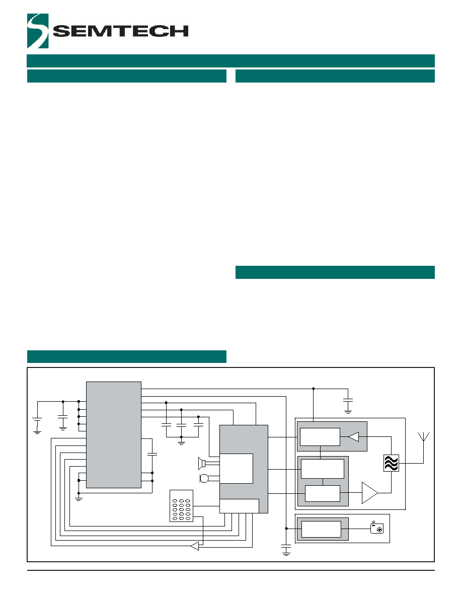
Typical Application Circuit
Applications
The SC900A is a highly integrated power management de-
vice for low power portable applications. The device con-
tains fi ve adjustable low-dropout linear regulators (LDOs)
with CMOS pass-devices as well as a band-gap reference,
I
2
C interface, and DACs to control the output voltages.
Many features of the SC900A are programmable through
the I
2
C interface. These include the ability to independent-
ly turn on any combination of the fi ve regulators. All fi ve
of the LDO output voltages are programmable in 50mV
steps from 1.45V to 3.00V for LDOs A and B, and from
1.75V to 3.30V for LDOs C, D and E. Each LDO can have
an active shutdown or nonactive shutdown program op-
tion through the interface. There is also a reset monitor
fl ag that is associated with LDOA. In addition, the device
has a separate programmable power good monitor fl ag
that activates when one or more LDOs go out of regula-
tion.
The SC900A offers signifi cant quiescent current and
space savings to the system designer by sharing refer-
ence and biasing among fi ve LDOs. The small and ther-
mally effi cient 20-lead MLPQ package make it ideal for
use in portable products where minimizing layout area is
critical.
Palmtop/Laptop computers
Personal Digital Assistants
Cellular telephones
Battery-powered equipment
High effi ciency linear power supplies
+
Keypad
VIN
INA
INB
INCD
INE
EN
LDOPGD
ARST
SDA
SCL
A0
GND
LDOE
LDOD
LDOA
LDOB
LDOC
VREF
VASEL
DGND
SC900A
2.2uF 2.2uF 2.2uF
2.2uF
2.2uF
0.1uF
4.7uF
VBAT
-
Baseband
Processor
Audio
Processing
Digital
Interface
PA
TCXO
&
Synthesiser
Transmitter
Section
Receiver
Section
LNA
Camera
Processing
CCD
2
© 2005 Semtech Corp.
www.semtech.com
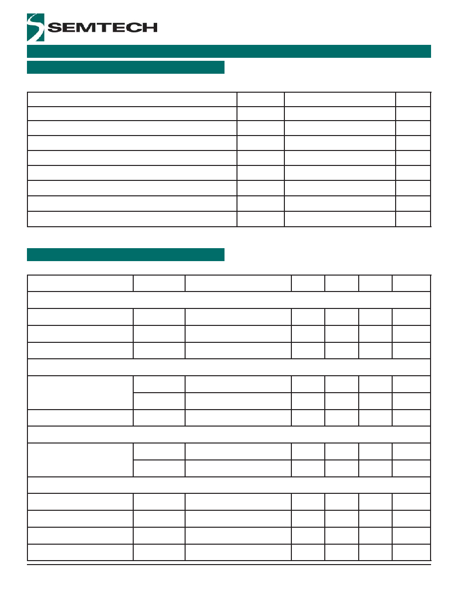
POWER MANAGEMENT
SC900A
Parameter
Symbol
Maximum
Units
Input Supply Voltage
V
IN
-0.3 to +7
V
Digital Input Voltage
V
DIG
-0.3 to VIN +0.3
V
Operating Ambient Temperature Range
T
A
-40 to +85
°C
Operating Junction Temperature Range
T
J
-40 to +125
°C
Peak IR Flow Temperature
T
LEAD
260
°C
Storage Temperature
T
STG
-60 to +150
°C
Thermal Impedance Junction to Ambient
(1)
JA
40
°C/W
ESD Protection Level
(2)
ESD
2
kV
Exceeding the specifi cations below may result in permanent damage to the device or device malfunction. Operation outside of the parameters specifi ed in the
Electrical Characteristics section is not implied.
Unless otherwise noted V
IN
= 3.7V, T
A
= -40 to +85
°
C. Typical values are at T
A
= +25
°
C.
(1) Calculated from package in still air, mounted to 3" x 4.5", 4 layer FR4 PCB with thermal vias under the exposed pad as per JESD51 standards.
(2) Tested according to JEDEC standard JESD22-A114-B.
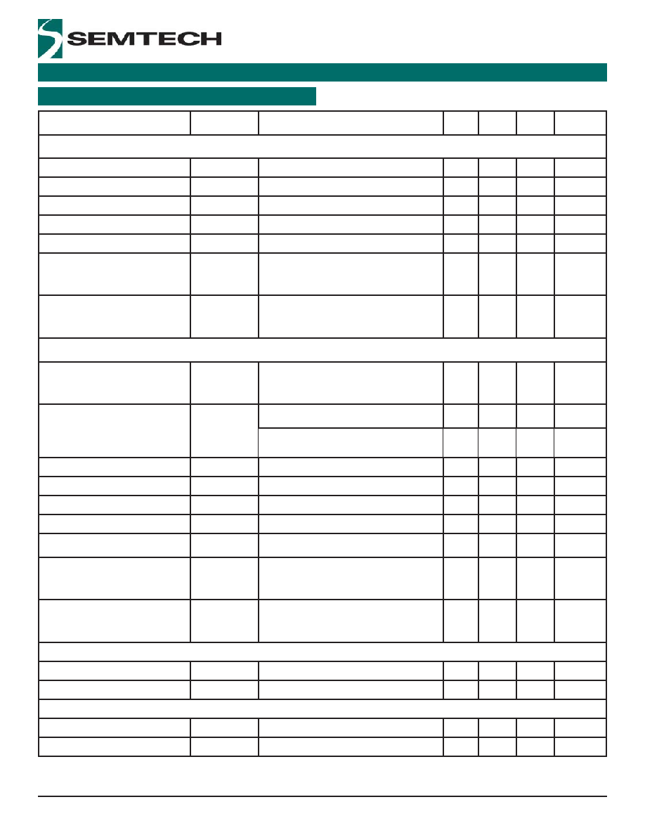
Electrical Characteristics
Absolute Maximum Ratings
Parameter
Symbol
Conditions
Min
Typ
Max
Units
General
Supply Voltage
V
IN
All outputs < VIN - dropout
2.7
5.5
V
Quiescent Current Shutdown
I
Q-SHUTDOWN
10
A
Supply Bypass Capacitor
C
VCC
Per input pin
1
F
Digital Inputs
Digital Input Voltage
V
IL
0.4
V
V
IH
1.6
V
Digital Input Current
I
DIG
-0.2
0.2
A
Digital Outputs
Digital Output Voltage
(1)
V
OL
I
SINK
= 1.2mA, V 1.8V
2
10
%LDOB
V
OH
I
SOURCE
= 0.5mA, V 1.8V
90
98
%LDOB
Referencing and Biasing Circuitry
Quiescent Current Reference
I
Q-REF
25
A
Reference Voltage
V
REF
1.227
V
V
REF
Start-Up Time
I
VREF
C
VREF
= 100nF
15
ms
V
REF
Bypass Capacitor
C
VREF
0.1
F
3
© 2005 Semtech Corp.
www.semtech.com
POWER MANAGEMENT
SC900A
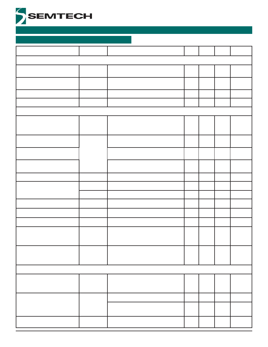
Electrical Characteristics (Cont.)
Parameter
Symbol
Conditions
Min
Typ
Max
Units
LDO Regulators
Quiescent Supply Current
I
Q
All LDOs active in
default states
190
360
A
Quiescent Supply Current
at Start-Up
I
QSUP
LDO A, B, C active in default states
V
OUT
+ 0.5V < V
IN
< 5.5V
125
A
Current Limit
I
LIM
250
410
650
mA
Bypass Capacitor
C
BYP
Ceramic, low ESR
2.2
F
LDO Regulator A (Core Supply)
Output Voltage Accuracy
VOA
A
1.45V V
OUT
3.00V
V
OUT
+ 0.2V V
IN
5.5V
I
OUT
= 1mA, T
A
= 25°C
-3
+3
%
Output Voltage Accuracy at
2.80V (DAC = 11011)
VOAS
A
I
OUT
= 1mA
-2
+2
%
Output Voltage Accuracy at
1.80V (DAC = 00011)
I
OUT
= 1mA, T
A
= 25°C
-3
+3
%
Output Voltage Accuracy at
2.80V (DAC = 11011)
V
OUT
+ 0.5V V
IN
5.5V,
I
OUT
= 200mA
-3.5
+3.5
%
Maximum Output Current
IOMAX
A
200
mA
Default Setting: ON
VO
A-HI
VASEL - High
2.80
V
VO
A-LO
VASEL - Low
1.80
V
Line Regulation at 1.8V, 2.8V
LINEREG
A
I
OUT
= 1mA, V
OUT
+ 0.2V < V
IN
< 5.5V
2.5
12
mV
Load Regulation at 1.8V, 2.8V
LOADREG
A
1mA < I
OUT
<200mA
-3
-20
mV
Dropout Voltage
V
DA
V
OUT
= 3.0V, I
OUT
= 200mA
200
250
mV
Power Supply Rejection Ratio
PSRR
A
f = 10Hz - 1kHz, C
BYP
= 0.1F,
I
OUT
= 50mA,
2.5V V
OUT
3.0V
60
dB
Output Voltage Noise
(2)
e
n-A
f = 10Hz - 100kHz, I
OUT
= 50mA,
C
VREF
= 0.1F, C
OUT
= 2.2F,
2.5V V
OUT
3.0V
45
V
RMS
LDO Regulator B (DIGITAL I/O SUPPLY)
Output Voltage Accuracy
VOA
B
1.45V V
OUT
3.00V
V
OUT
+ 0.15V V
IN
5.5V
I
OUT
= 1mA, T
A
= 25°C
-3
+3
%
Output Voltage Accuracy at
2.80V (DAC = 11011)
VOAS
B
I
OUT
= 1mA
-2
+2
%
V
OUT
+ 0.5V V
IN
5.5V,
I
OUT
= 150mA
-3.5
+3.5
%
Maximum Output Current
IOMAX
B
150
mA
4
© 2005 Semtech Corp.
www.semtech.com
POWER MANAGEMENT
SC900A
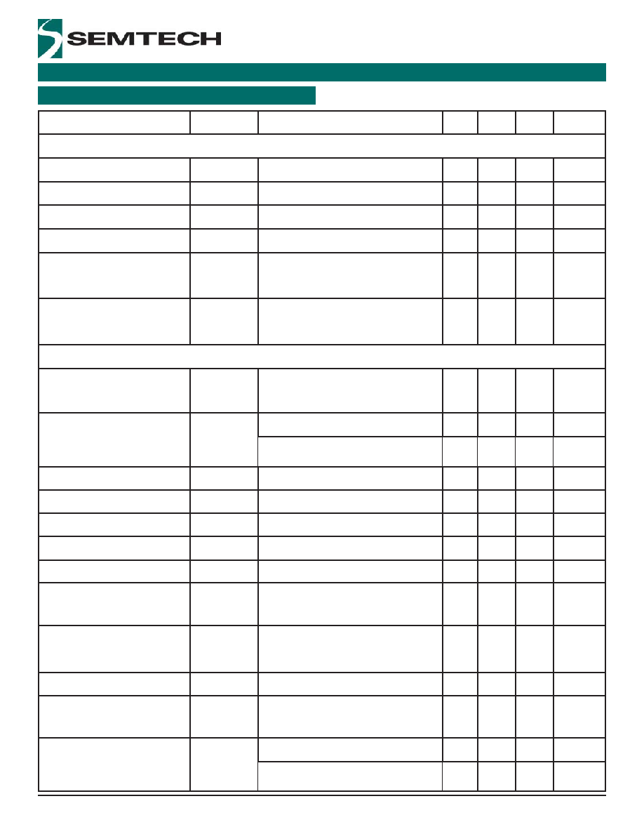
Electrical Characteristics (Cont.)
Parameter
Symbol
Conditions
Min
Typ
Max
Units
LDO Regulator B (DIGITAL I/O SUPPLY) (Cont.)
Default Setting: ON
VO
B
2.80
mV
Line Regulation at 2.8V
LINEREG
B
I
OUT
= 1mA, V
OUT
+ 0.15V < V
IN
< 5.5V
2.5
12
mV
Load Regulation at 2.8V
LOADREG
B
1mA < I
OUT
<150mA
-3
20
mV
Dropout Voltage
V
DB
V
OUT
= 3.0V, I
OUT
= 150mA
150
190
mV
Power Supply Rejection Ratio
PSRR
B
f = 10Hz - 1kHz, C
BYP
= 0.1F,
I
OUT
= 50mA,
2.5V V
OUT
3.0V
60
dB
Output Voltage Noise
(2)
e
n-B
f = 10Hz - 100kHz, I
OUT
= 50mA,
C
VREF
= 0.1F, C
OUT
= 2.2F,
2.5V V
OUT
3.0V
45
V
RMS
LDO Regulator C
Output Voltage Accuracy
VOA
C
1.75V V
OUT
3.30V
V
OUT
+ 0.15V V
IN
5.5V
I
OUT
= 1mA, T
A
= 25°C
-3
+3
%
Output Voltage Accuracy at
2.90V (DAC = 10111)
VOAS
C
I
OUT
= 1mA
-2
+2
%
V
OUT
+ 0.5V V
IN
5.5V,
I
OUT
= 150mA
-3.5
+3.5
%
Maximum Output Current
IOMAX
C
150
mA
Default Setting: ON
VO
C
2.90
V
Line Regulation at 2.90V
LINEREG
C
I
OUT
= 1mA, V
OUT
+ 0.15V < V
IN
< 5.5V
2.5
12
mV
Load Regulation at 2.90V
LOADREG
C
1mA < I
OUT
<150mA
-3
-20
mV
Dropout Voltage
V
DC
V
OUT
= 3.3V, I
OUT
= 150mA
150
190
mV
Power Supply Rejection Ratio
PSRR
C
f = 10Hz - 1kHz, C
BYP
= 0.1F,
I
OUT
= 50mA,
2.5V V
OUT
3.3V
60
dB
Output Voltage Noise
(2)
e
n-C
f = 10Hz - 100kHz, I
OUT
= 50mA,
C
VREF
= 0.1F, C
OUT
= 2.2F,
2.5V V
OUT
3.3V
55
V
RMS
LDO Regulator D
Output Voltage Accuracy
VOA
D
1.75V V
OUT
3.30V
V
OUT
+ 0.15V V
IN
5.5V
I
OUT
= 1mA, T
A
= 25°C
-3
+3
%
Output Voltage Accuracy at
3.10V (DAC = 10111)
VOAS
D
I
OUT
= 1mA
-2
+2
%
V
OUT
+ 0.5V V
IN
5.5V,
I
OUT
= 150mA
-3.5
+3.5
%
5
© 2005 Semtech Corp.
www.semtech.com
POWER MANAGEMENT
SC900A
Electrical Characteristics (Cont.)
Parameter
Symbol
Conditions
Min
Typ
Max
Units
LDO Regulator D (Cont.)
Maximum Output Current
IOMAX
D
150
mA
Default Setting: OFF
VO
D
3.10
V
Line Regulation at 3.10V
LINEREG
D
I
OUT
= 1mA, V
OUT
+ 0.15V < V
IN
< 5.5V
2.5
12
mV
Load Regulation at 3.10V
LOADREG
D
1mA < I
OUT
<150mA
-3
-20
mV
Dropout Voltage
V
DD
V
OUT
= 3.3V, I
OUT
= 150mA
150
190
mV
Power Supply Rejection Ratio
PSRR
D
f = 10Hz - 1kHz, C
BYP
= 0.1mF,
I
OUT
= 50mA,
2.5V V
OUT
3.3V
60
dB
Output Voltage Noise
(2)
e
n-D
f = 10Hz - 100kHz, I
OUT
= 50mA,
C
VREF
= 0.1F, C
OUT
= 2.2F,
2.5V V
OUT
3.3V
55
V
RMS
LDO Regulator E
Output Voltage Accuracy
VOA
E
1.75V V
OUT
3.30V
V
OUT
+ 0.15V V
IN
5.5V
I
OUT
= 1mA, T
A
= 25°C
-3
+3
%
Output Voltage Accuracy at
3.10V (DAC = 10111)
VOAS
E
I
OUT
= 1mA
-2
+2
%
V
OUT
+ 0.5V V
IN
5.5V,
I
OUT
= 150mA
-3.5
+3.5
%
Maximum Output Current
IOMAX
E
150
mA
Default Setting: OFF
VO
E
3.10
V
Line Regulation at 3.10V
LINEREG
E
I
OUT
= 1mA, V
OUT
+ 0.15V < V
IN
< 5.5V
2.5
12
mV
Load Regulation at 3.10V
LOADREG
E
1mA < I
OUT
= 150mA
-3
-20
mV
Dropout Voltage
V
DE
V
OUT
= 3.3V, I
OUT
= 150mA
150
190
mV
Power Supply Rejection Ratio
PSRR
E
f = 10Hz - 1kHz, C
BYP
= 0.1F,
I
OUT
= 50mA,
2.5V V
OUT
3.3V
60
dB
Output Voltage Noise
(2)
e
n-E
f = 10Hz - 100kHz, I
OUT
= 50mA,
C
VREF
= 0.1F, C
OUT
= 2.2F,
2.5V V
OUT
3.3V
55
V
RMS
A RESET
Reset Threshold
RESET
THLD
77
%
Reset Active Timeout Delay
t
RD
Delay in default state
75
100
125
ms
LDO POWER GOOD
PGOOD Threshold
PGOOD
THLD
77
%
PGOOD Active Timeout Delay
t
PG
Delay in default state
75
100
125
ms
Notes:
1) Digital outputs are powered from LDOB, so LDOB must be active for operation of LDOPGD and ARST.
2) Below 2.5V: becomes digital regulator.