SC905.indd
www.semtech.com
1
POWER MANAGEMENT
SC905
CDMA Cellular Phone
Power Management IC
October 26, 2005
Description
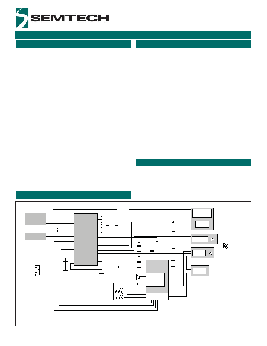
The SC905 is a power management integrated circuit
(PMIC) designed for the latest CDMA chip sets. The device
provides four general purpose low dropout regulators
(LDOs), and fi ve low noise LDOs designed for analog cir-
cuits. The VMOT LDO can be used as a general purpose
regulator or
as an adjustable motor drive output that can
supply up to 150mA to drive a vibrator motor.
Each LDOs enable and output voltage are controlled via
the I
2
C bus. An option
al t
hree-wire interfa
ce c
ompatible
with Semtech battery charger I
Cs i
s also controlled via the
I
2
C bus.
Initial power-on is achieved by activating either the ON or
the HFPWR signal, and the PGOOD input is used by the
microprocessor to latch power on o
r
disable the device.
The small and thermally effi cient MLPQ-32 package and
use of ceramic bypass capacitor
s,
minimize the required
PCB area making the SC905 ideal for space-conscious
portable applications.
9 LDO Linear Regulators
CORE: 1.35V - 2.90V @ 300mA
ANA: 2.55V - 2.90V @ 200mA
PAD: 1.35V - 2.90V @ 300mA
RX: 2.55V - 2.90V @ 150mA
TX: 2.55V - 2.90V @ 150mA
TCXO: 2.55V - 2.90V @ 80mA
PLL: 2.55V - 2.90V @ 80mA
Camera: 1.35V - 2.90V @ 100mA
Motor Drive: 1.35V - 2.90V @ 150mA
I
2
C Interface for Microprocessor Control
Less than 1A Quiescent Current in Shutdown
65dB PSRR for Analog LDOs
Over-Temperature Protection
Power-On Control
Optional Interface for Controlling Semtech
Battery
Chargers
Small 5mm x 5mm 32-Pin QFN Package
CDMA Cellular Handsets
Palmtop/Laptop Computers
Battery Powered Equipment
10F
VBAT
MOTOR
0.1F
ON/OFF
1F
Keypad
Baseband
Processor
Audio
Processing
Digital
Interface
Camera
Module
TCXO
+
Synthesiser
PLL
Transmitter
Section
PA
Receiver
Section
LNA
SC905
VBAT
IN1
IN2
IN3
IN4
IN5
IN6
DVIN
VCORE
VPAD
VANA
VTCXO
VTX
VRX
VCAM
VPLL
VPSEL
VCSEL
DGND
CPB
CHRGB
FAULTB
AGND
BP
VMOT
RESB
PWRON
SCL
PGOOD
HFPWR
ON
SDA
BATTERY
Handsfree
Option
Battery
Charger
Circuit
1F
1F
1F
1F
1F
1F
1F
Features
Typical Application Circuit
Applications
2
� 2005 Semtech Corp.
www.semtech.com
POWER MANAGEMENT
SC905
Exceeding the specifi cations below may result in permanent damage to the device or device malfunction. Operation outside of the parameters specifi ed in the
Electrical Characteristics section is not implied.
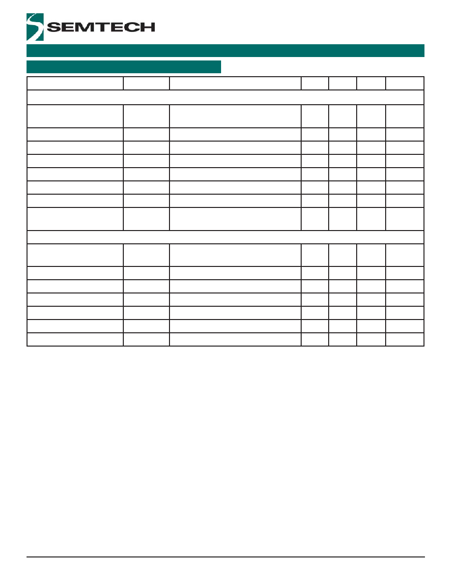
Parameter
Symbol
Maximum
Units
Input Supply Voltage
V
IN
-0.3 to +7
V
Digital Input Voltage
V
DIG
-0.3 to V
IN
+0.3
V
Operating Ambient Temperature Range
T
A
-40 to +85
�C
Operating Junction Temperature Range
T
J
-40 to +125
�C
Peak IR Refl ow Temperature
T
LEAD
260
�C
Storage Temperature
T
STG
-60 to +150
�C
Thermal Resistance Junction to Ambient
(1)
JA
36
�C/W
ESD Protection Level
(2)
ESD
2
kV
Unless otherwise noted V
IN
= 3.7V, T
A
= -40 to +85
�
C. Typical values are at T
A
= +25
�
C.
Parameter
Symbol
Condition
Min
Typ
Max
Units
General
Supply Voltage
V
IN
2.7
5.5
V
Shutdown Current
I
SD
ON = 0V, HFPWR = 0V, PGOOD = 0V
1
A
Quiescent Supply Current
I
SU
Default Start-up Mode
300
A
I
STBY
I
2
C, V
REF
Active, All Outputs Disabled
30
60
A
Supply Bypass Capacitor
C
VCC
At Each Power Input Pin
1
F
Start-Up Time
t
SU
C
BP
= 0.1F
25
ms
Under-Voltage Lockout
UVLO
Descending, Hysteresis = 50mV
2.5
V
Over-Temperature
OT
Hysteresis = 20�C
160
�C
Digital Inputs
Digital Input Voltage
(1)
V
IL
0.4
V
V
IH
1.25
V
Digital Input Current
I
DIG
Logic Level High or Low
-0.2
0.2
A
Digital Outputs
Digital Output Voltage
(2)
V
OL
I
SINK
= 1.2mA
2
10
%VPAD
V
OH
I
SOURCE
= 0.5mA, VPAD 1.8V
90
98
%VPAD
LDO Regulator (CORE) - 300mA
Output Voltage Accuracy
(3)
V
OUT
1.35V V
OUT
2.90V, I
OUT
= 1mA,
V
OUT
+0.35V V
IN
5.5V
-75
+75
mV
Current Limit
I
LIM
V
CORE
= 0V
350
900
mA
Default At Start-Up: ON
V
OUT-HI
VCSEL - High
1.80
V
V
OUT-LO
VCSEL - Low
1.35
V
(1) Calculated from package in still air, mounted to 3" x 4.5", 4 layer FR4 PCB with thermal vias under the exposed pad as per JESD51 standards.
(2) Tested according to JEDEC standard JESD22-A114-B.
Electrical Characteristics
Absolute Maximum Ratings
3
� 2005 Semtech Corp.
www.semtech.com
POWER
MANAGEMENT
SC905
Parameter
Symbol
Condition
Min
Typ
Max
Units
LDO Regulator (CORE) - 300mA (Cont.)
Line Regulation
REG
LINE
I
OUT
= 1mA, V
OUT
+0.35V < V
IN
< 5.5V
2.5
12
mV
Load Regulation
REG
LOAD
1mA < I
OUT
< 300mA
-3
-30
mV
Dropout Voltage
V
DO
V
OUT
= 2.90V, I
OUT
= 300mA
300
350
mV
Power Supply Rejection Ratio
PSRR
CORE
f = 10Hz - 1kHz, C
OUT
= 1F, I
OUT
= 50mA
50
dB
LDO Regulator (PAD) - 300mA
Output Voltage Accuracy
(3)
V
OUT
1.35V V
OUT
2.90V, I
OUT
=1mA,
V
OUT
+0.35V V
IN
5.5V
-75
+75
mV
Current Limit
I
LIM
V
PAD
= 0V
350
900
mA
Default at Start-up: ON
V
OUT-HI
VPSEL - High
2.60
V
V
OUT-LO
VPSEL - Low
1.80
V
Line Regulation
REG
LINE
I
OUT
= 1mA, V
OUT
+0.35V < V
IN
< 5.5V
2.5
12
mV
Load Regulation
REG
LOAD
1mA < I
OUT
< 300mA
-3
-30
mV
Dropout Voltage
V
DO
V
OUT
= 2.90V, I
OUT
= 300mA
300
350
mV
Power Supply Rejection Ratio
PSRR
PAD
f = 10Hz - 1kHz, C
OUT
= 1F, I
OUT
= 50mA
50
dB
LDO Regulator (ANA) - 200mA
Output Voltage Accuracy
(4)
V
OUT
2.55V
V
OUT
2.90V, I
OUT
= 1mA,
V
OUT
+0.35V
V
IN
5.5V
-75
+75
mV
Current Limit
I
LIM
V
ANA
= 0V
250
650
mA
Default At Start-up: ON
V
OUT
2.60
V
Line Regulation
REG
LINE
I
OUT
= 1mA, V
OUT
+0.35V < V
IN
< 5.5V
2.5
12
mV
Load Regulation
REG
LOAD
1mA < I
OUT
< 200mA
-3
-20
mV
Dropout Voltage
V
DO
V
OUT
= 2.90V, I
OUT
= 200mA
200
250
mV
Power Supply Rejection Ratio
PSRR
ANA
f = 10Hz - 1kHz, C
OUT
= 1F, I
OUT
= 50mA
65
dB
Output Voltage Noise
e
n
f = 10Hz to 100kHz, I
OUT
= 50mA,
C
BP
= 0.1F, C
OUT
= 1F
45
V
RMS
LDO Regulator (TCXO) - 80mA
Output Voltage Accuracy
(4)
V
OUT
2.55V V
OUT
2.90V, I
OUT
= 1mA,
V
OUT
+0.35V
V
IN
5.5V
-75
+75
mV
Current Limit
I
LIM
V
TCXO
= 0V
250
650
mA
Default At Start-up: ON
V
OUT
2.85
V
Line Regulation
REG
LINE
I
OUT
= 1mA, V
OUT
+0.35V < V
IN
< 5.5V
2.5
12
mV
Load Regulation
REG
LOAD
1mA < I
OUT
< 80mA
-3
-20
mV
Dropout Voltage
V
DO
V
OUT
= 2.90V, I
OUT
= 80mA
200
250
mV
Power Supply Rejection Ratio
PSRR
TCXO
f = 10Hz - 1kHz, C
OUT
= 1F, I
OUT
= 50mA
65
dB
Electrical Characteristics (Cont.)
4
� 2005 Semtech Corp.
www.semtech.com
POWER MANAGEMENT
SC905
Parameter
Symbol
Condition
Min
Typ
Max
Units
LDO Regulator (TCXO) - 80mA (Cont.)
Output Voltage Noise
e
n
f = 10Hz - 100kHz, I
OUT
= 50mA,
C
BP
= 0.1F, C
OUT
= 1F
45
V
RMS
LDO Regulator (TX) - 150mA
Output Voltage Accuracy
(4)
V
OUT
2.55V V
OUT
2.90V, I
OUT
= 1mA,
V
OUT
+0.35V
V
IN
5.5V
-75
+75
mV
Current Limit
I
LIM
V
TX
= 0V
250
650
mA
Default At Start-up: OFF
V
OUT
2.85
V
Line Regulation
REG
LINE
I
OUT
= 1mA, V
OUT
+0.35V < V
IN
< 5.5V
2.5
12
mV
Load Regulation
REG
LOAD
1mA < I
OUT
< 150mA
-3
-20
mV
Dropout Voltage
V
DO
V
OUT
= 2.90V, I
OUT
= 150mA
200
250
mV
Power Supply Rejection Ratio
PSRR
TX
f = 10Hz - 1kHz, C
OUT
= 1F, I
OUT
= 50mA
65
dB
Output Voltage Noise
e
n
f = 10Hz - 100kHz, I
OUT
= 50mA,
C
BP
= 0.1F, C
OUT
= 1F
45
V
RMS
LDO Regulator (RX) - 150mA
Output Voltage Accuracy
(4)
V
OUT
2.55V V
OUT
2.90V, I
OUT
= 1mA,
V
OUT
+0.35V
V
IN
5.5V
-75
+75
mV
Current Limit
I
LIM
V
RX
= 0V
250
650
mA
Default At Start-up: OFF
V
OUT
2.85
V
Line Regulation
REG
LINE
I
OUT
= 1mA, V
OUT
+0.35V < V
IN
< 5.5V
2.5
12
mV
Load Regulation
REG
LOAD
1mA < I
OUT
< 150mA
-3
-20
mV
Dropout Voltage
V
DO
V
OUT
= 2.90V, I
OUT
= 150mA
200
250
mV
Power Supply Rejection Ratio
PSRR
RX
f = 10Hz - 1kHz, C
OUT
= 1F, I
OUT
= 50mA
65
dB
Output Voltage Noise
e
n
f = 10Hz - 100kHz, I
OUT
= 50mA,
C
BP
= 0.1F, C
OUT
= 1F
45
V
RMS
LDO Regulator (CAM) - 100mA
Output Voltage Accuracy
(3)
V
OUT
1.35V V
OUT
2.90V, I
OUT
= 1mA
V
OUT
+0.35V
V
IN
5.5V
-75
+75
mV
Current Limit
I
LIM
V
CAM
= 0V
250
650
mA
Default At Start-up: OFF
V
OUT
1.80
V
Line Regulation
REG
LINE
I
OUT
= 1mA, V
OUT
+0.35V < V
IN
< 5.5V
2.5
12
mV
Load Regulation
REG
LOAD
1mA < I
OUT
< 100mA
-3
-20
mV
Dropout Voltage
V
DO
V
OUT
= 2.90V, I
OUT
= 100mA
200
250
mV
Power Supply Rejection Ratio
PSRR
CAM
f = 10Hz - 1kHz, C
OUT
= 1F, I
OUT
= 50mA
50
dB
Electrical Characteristics (Cont.)
5
� 2005 Semtech Corp.
www.semtech.com
POWER
MANAGEMENT
SC905
Parameter
Symbol
Condition
Min
Typ
Max
Units
LDO Regulator (PLL) - 80mA
Output Voltage Accuracy
(4)
V
OUT
2.55V V
OUT
2.90V, I
OUT
= 1mA,
V
OUT
+0.35V
V
IN
5.5V
-75
+75
mV
Current Limit
I
LIM
V
PLL
= 0V
250
650
mA
Default At Start Up: OFF
V
OUT
2.85
V
Line Regulation
REG
LINE
I
OUT
= 1mA, V
OUT
+0.35V < V
IN
< 5.5V
2.5
12
mV
Load Regulation
REG
LOAD
1mA < I
OUT
< 80mA
-3
-20
mV
Dropout Voltage
V
DO
V
OUT
= 2.90V, I
OUT
= 80mA
200
250
mV
Power Supply Rejection Ratio
PSRR
PLL
f = 10Hz - 1kHz, C
OUT
= 1F, I
OUT
= 50mA
65
dB
Output Voltage Noise
e
n
f = 10Hz - 100kHz, I
OUT
= 50mA,
C
BP
= 0.1F, C
OUT
= 1F
45
V
RMS
LDO Regulator (MOT) - 150mA
Output Voltage Accuracy
(3)
V
OUT
1.35V V
OUT
2.90V, I
OUT
= 1mA,
V
OUT
+0.35V
V
IN
5.5V
-75
+75
mV
Current Limit
I
LIM
V
MOT
= 0V
250
650
mA
Default at Start Up: OFF
V
OUT
1.40
V
Line Regulation
REG
LINE
I
OUT
= 1mA, V
OUT
+0.35V < V
IN
< 5.5V
2.5
12
mV
Load Regulation
REG
LOAD
1mA < I
OUT
< 150mA
-3
-20
mV
Dropout Voltage
V
DO
V
OUT
= 2.90V, I
OUT
= 150mA
200
250
mV
Power Supply Rejection Ratio
PSRR
MOT
f = 10Hz - 1kHz, C
OUT
= 1F, I
OUT
= 50mA
50
dB
Electrical Characteristics (Cont.)