 | –≠–ª–µ–∫—Ç—Ä–æ–Ω–Ω—ã–π –∫–æ–º–ø–æ–Ω–µ–Ω—Ç: SC905A | –°–∫–∞—á–∞—Ç—å:  PDF PDF  ZIP ZIP |

www.semtech.com
1
POWER MANAGEMENT
SC905A
CDMA Cellular Phone
Power Management IC
January 24, 2006
Description
The SC905A is a power management integrated circuit
(PMIC) designed for the latest CDMA chip sets. The device
provides four general purpose low dropout regulators
(LDOs), and five low noise LDOs designed for analog
circuits. The VMOT LDO can be used as a general purpose
regulator or
as an adjustable motor drive output that can
supply up to 150mA to drive a vibrator motor.
Each LDO's enable and output voltage are controlled via
the I
2
C bus. The VTCXO output has an external enable pin
that can be used instead of the register bit when timing is
critical for minimizing sleep current. The VMOT also has
an external enable pin for additional fl exibility.
Initial power-on is achieved by activating either the ON
button, the battery charger, or the HFPWR signal, and the
PGOOD input is used by the microprocessor to latch power
on o
r
disable the device.
The thermally-effi cient MLPQ-32 package combined with
miniature ceramic bypass capacitors minimize required
PCB area, making the SC905A ideal for space-conscious
portable applications.
9 LDO Linear Regulators
CORE: 1.35V - 2.90V @ 300mA
ANA: 2.55V - 2.90V @ 200mA
PAD: 1.75V - 3.30V @ 300mA
RX: 2.75V - 3.10V @ 150mA
TX: 2.75V - 3.10V @ 150mA
TCXO: 2.75V - 3.10V @ 80mA
PLL: 2.75V - 3.10V @ 80mA
Camera: 1.75V - 3.30V @ 100mA
Motor Drive: 1.75V - 3.30V @ 150mA
I
2
C Interface for Microprocessor Control
Less than 1A Quiescent Current in Shutdown
65dB PSRR for Analog LDOs
Over-Temperature Protection
Power-On Control
Small 5mm x 5mm 32-Pin MLPQ Package
CDMA Cellular Handsets
PDAs/Smartphones
Wireless VOIP Handsets
Features
Typical Application Circuit
Applications
10F
VBAT
MOTOR
0. 1F
ON/OFF
1 F
Keypad
Baseband
Processor
Audio
Processing
Digital
Interface
Camera
Module
TCXO
+
Synthesiser
PLL
Transmitter
Section
PA
Receiver
Section
LNA
SC905A
VBAT
IN 1
IN 2
IN 3
IN 4
IN 5
IN 6
DVIN
VCORE
VPAD
VANA
VTCXO
VTX
VRX
VCAM
VPLL
VPSEL
VCSEL
DGND
CHPWR
EN_TCXO
EN_MOT
AGND
BP
VMOT
RESB
PWRON
SCL
PGOOD
HFPWR
ON
SDA
B A TTE RY
Handsfree
Option
Battery
Charger
Circuit
1F
1F
1F
1F
1F
1 F
1F

2
© 2006 Semtech Corp.
www.semtech.com
POWER MANAGEMENT
SC905A
Exceeding the specifi cations below may result in permanent damage to the device or device malfunction. Operation outside of the parameters specifi ed in the
Electrical Characteristics section is not implied.
Parameter
Symbol
Maximum
Units
Input Supply Voltage
V
IN
-0.3 to +7
V
Digital Input Voltage
V
DIG
-0.3 to V
IN
+0.3
V
Operating Ambient Temperature Range
T
A
-40 to +85
∞C
Operating Junction Temperature Range
T
J
-40 to +125
∞C
Peak IR Refl ow Temperature
T
LEAD
260
∞C
Storage Temperature
T
STG
-60 to +150
∞C
Thermal Resistance Junction to Ambient
(1)
JA
26
∞C/W
ESD Protection Level
(2)
ESD
2
kV
Unless otherwise noted V
IN
= 3.7V, T
A
= -40 to +85
∞
C. Typical values are at T
A
= +25
∞
C.
Parameter
Symbol
Condition
Min
Typ
Max
Units
General
Supply Voltage
V
IN
2.7
5.5
V
Shutdown Current
I
SD
ON = 0V, HFPWR = 0V, CHPWR = 0V,
PGOOD = 0V
1
A
Quiescent Supply Current
I
SU
Default Start-Up Mode
300
A
I
STBY
I
2
C, V
REF
Active, All Outputs Disabled
30
60
A
Supply Bypass Capacitor
C
VCC
At Each Power Input Pin
1
F
Start-Up Time
t
SU
C
BP
= 0.1F
25
ms
Under-Voltage Lockout
UVLO
Descending, Hysteresis = 50mV
2.5
V
Over-Temperature
OT
Hysteresis = 20∞C
160
∞C
Digital Inputs
Digital Input Voltage
(1)
V
IL
0.4
V
V
IH
1.25
V
Digital Input Current
I
DIG
Logic Level High or Low
-0.2
0.2
A
Digital Outputs
Digital Output Voltage
(2)
V
OL
I
SINK
= 1.2mA
2
10
%VPAD
V
OH
I
SOURCE
= 0.5mA, VPAD 1.8V
90
98
%VPAD
LDO Regulator (CORE) - 300mA
Output Voltage Accuracy
(3)
V
OUT
1.35V V
OUT
2.90V, I
OUT
= 1mA,
V
OUT
+0.35V V
IN
5.5V
-75
+75
mV
Current Limit
I
LIM
V
CORE
= 0V
350
900
mA
Default At Start-Up: ON
V
OUT-HI
VCSEL - High
1.80
V
V
OUT-LO
VCSEL - Low
1.35
V
Notes:
(1) Calculated from package in still air, mounted to 3" x 4.5", 4 layer FR4 PCB with thermal vias under the exposed pad as per JESD51 standards.
(2) Tested according to JEDEC standard JESD22-A114-B.
Electrical Characteristics
Absolute Maximum Ratings

3
© 2006 Semtech Corp.
www.semtech.com
POWER MANAGEMENT
SC905A
Parameter
Symbol
Condition
Min
Typ
Max
Units
LDO Regulator (CORE) - 300mA (Cont.)
Line Regulation
REG
LINE
I
OUT
= 1mA, V
OUT
+0.35V < V
IN
< 5.5V
2.5
12
mV
Load Regulation
REG
LOAD
1mA < I
OUT
< 300mA
-3
-30
mV
Dropout Voltage
V
DO
V
OUT
= 2.90V, I
OUT
= 300mA
300
350
mV
Power Supply Rejection Ratio
PSRR
CORE
f = 10Hz - 1kHz, C
OUT
= 1F, I
OUT
= 50mA
50
dB
LDO Regulator (PAD) - 300mA
Output Voltage Accuracy
(3)
V
OUT
1.75V V
OUT
3.30V, I
OUT
=1mA,
V
OUT
+0.35V V
IN
5.5V
-75
+75
mV
Current Limit
I
LIM
V
PAD
= 0V
350
900
mA
Default at Start-Up: ON
V
OUT-HI
VPSEL - High
3.00
V
V
OUT-LO
VPSEL - Low
2.20
V
Line Regulation
REG
LINE
I
OUT
= 1mA, V
OUT
+0.35V < V
IN
< 5.5V
2.5
12
mV
Load Regulation
REG
LOAD
1mA < I
OUT
< 300mA
-3
-30
mV
Dropout Voltage
V
DO
V
OUT
= 3.30V, I
OUT
= 300mA
300
350
mV
Power Supply Rejection Ratio
PSRR
PAD
f = 10Hz - 1kHz, C
OUT
= 1F, I
OUT
= 50mA
50
dB
LDO Regulator (ANA) - 200mA
Output Voltage Accuracy
(4)
V
OUT
2.55V
V
OUT
2.90V, I
OUT
= 1mA,
V
OUT
+0.35V
V
IN
5.5V
-75
+75
mV
Current Limit
I
LIM
V
ANA
= 0V
250
650
mA
Default At Start-Up: ON
V
OUT
2.60
V
Line Regulation
REG
LINE
I
OUT
= 1mA, V
OUT
+0.35V < V
IN
< 5.5V
2.5
12
mV
Load Regulation
REG
LOAD
1mA < I
OUT
< 200mA
-3
-20
mV
Dropout Voltage
V
DO
V
OUT
= 2.90V, I
OUT
= 200mA
200
250
mV
Power Supply Rejection Ratio
PSRR
ANA
f = 10Hz - 1kHz, C
OUT
= 1F, I
OUT
= 50mA
65
dB
Output Voltage Noise
e
n
f = 10Hz to 100kHz, I
OUT
= 50mA,
C
BP
= 0.1F, C
OUT
= 1F
45
V
RMS
LDO Regulator (TCXO) - 80mA
Output Voltage Accuracy
(4)
V
OUT
2.75V V
OUT
3.10V, I
OUT
= 1mA,
V
OUT
+0.35V
V
IN
5.5V
-75
+75
mV
Current Limit
I
LIM
V
TCXO
= 0V
250
650
mA
Default At Start-Up: ON
V
OUT
3.05
V
Line Regulation
REG
LINE
I
OUT
= 1mA, V
OUT
+0.35V < V
IN
< 5.5V
2.5
12
mV
Load Regulation
REG
LOAD
1mA < I
OUT
< 80mA
-3
-20
mV
Dropout Voltage
V
DO
V
OUT
= 3.10V, I
OUT
= 80mA
200
250
mV
Power Supply Rejection Ratio
PSRR
TCXO
f = 10Hz - 1kHz, C
OUT
= 1F, I
OUT
= 50mA
65
dB
Output Voltage Noise
e
n
f = 10Hz - 100kHz, I
OUT
= 50mA,
C
BP
= 0.1F, C
OUT
= 1F
45
V
RMS
Electrical Characteristics (Cont.)

4
© 2006 Semtech Corp.
www.semtech.com
POWER MANAGEMENT
SC905A
Parameter
Symbol
Condition
Min
Typ
Max
Units
LDO Regulator (TX) - 150mA
Output Voltage Accuracy
(4)
V
OUT
2.75V V
OUT
3.10V, I
OUT
= 1mA,
V
OUT
+0.35V
V
IN
5.5V
-75
+75
mV
Current Limit
I
LIM
V
TX
= 0V
250
650
mA
Default At Start-Up: OFF
V
OUT
3.05
V
Line Regulation
REG
LINE
I
OUT
= 1mA, V
OUT
+0.35V < V
IN
< 5.5V
2.5
12
mV
Load Regulation
REG
LOAD
1mA < I
OUT
< 150mA
-3
-20
mV
Dropout Voltage
V
DO
V
OUT
= 3.10V, I
OUT
= 150mA
200
250
mV
Power Supply Rejection Ratio
PSRR
TX
f = 10Hz - 1kHz, C
OUT
= 1F, I
OUT
= 50mA
65
dB
Output Voltage Noise
e
n
f = 10Hz - 100kHz, I
OUT
= 50mA,
C
BP
= 0.1F, C
OUT
= 1F
45
V
RMS
LDO Regulator (RX) - 150mA
Output Voltage Accuracy
(4)
V
OUT
2.75V V
OUT
3.10V, I
OUT
= 1mA,
V
OUT
+0.35V
V
IN
5.5V
-75
+75
mV
Current Limit
I
LIM
V
RX
= 0V
250
650
mA
Default At Start-Up: OFF
V
OUT
3.05
V
Line Regulation
REG
LINE
I
OUT
= 1mA, V
OUT
+0.35V < V
IN
< 5.5V
2.5
12
mV
Load Regulation
REG
LOAD
1mA < I
OUT
< 150mA
-3
-20
mV
Dropout Voltage
V
DO
V
OUT
= 3.10V, I
OUT
= 150mA
200
250
mV
Power Supply Rejection Ratio
PSRR
RX
f = 10Hz - 1kHz, C
OUT
= 1F, I
OUT
= 50mA
65
dB
Output Voltage Noise
e
n
f = 10Hz - 100kHz, I
OUT
= 50mA,
C
BP
= 0.1F, C
OUT
= 1F
45
V
RMS
LDO Regulator (CAM) - 100mA
Output Voltage Accuracy
(3)
V
OUT
1.75V V
OUT
3.30V, I
OUT
= 1mA
V
OUT
+0.35V
V
IN
5.5V
-75
+75
mV
Current Limit
I
LIM
V
CAM
= 0V
250
650
mA
Default At Start-Up: OFF
V
OUT
2.20
V
Line Regulation
REG
LINE
I
OUT
= 1mA, V
OUT
+0.35V < V
IN
< 5.5V
2.5
12
mV
Load Regulation
REG
LOAD
1mA < I
OUT
< 100mA
-3
-20
mV
Dropout Voltage
V
DO
V
OUT
= 3.30V, I
OUT
= 100mA
200
250
mV
Power Supply Rejection Ratio
PSRR
CAM
f = 10Hz - 1kHz, C
OUT
= 1F, I
OUT
= 50mA
50
dB
LDO Regulator (PLL) - 80mA
Output Voltage Accuracy
(4)
V
OUT
2.75V V
OUT
3.10V, I
OUT
= 1mA,
V
OUT
+0.35V
V
IN
5.5V
-75
+75
mV
Current Limit
I
LIM
V
PLL
= 0V
250
650
mA
Electrical Characteristics (Cont.)

5
© 2006 Semtech Corp.
www.semtech.com
POWER MANAGEMENT
SC905A
Parameter
Symbol
Condition
Min
Typ
Max
Units
Default At Start-Up: OFF
V
OUT
3.05
V
Line Regulation
REG
LINE
I
OUT
= 1mA, V
OUT
+0.35V < V
IN
< 5.5V
2.5
12
mV
Load Regulation
REG
LOAD
1mA < I
OUT
< 80mA
-3
-20
mV
Dropout Voltage
V
DO
V
OUT
= 3.10V, I
OUT
= 80mA
200
250
mV
Power Supply Rejection Ratio
PSRR
PLL
f = 10Hz - 1kHz, C
OUT
= 1F, I
OUT
= 50mA
65
dB
Output Voltage Noise
e
n
f = 10Hz - 100kHz, I
OUT
= 50mA,
C
BP
= 0.1F, C
OUT
= 1F
45
V
RMS
LDO Regulator (MOT) - 150mA
Output Voltage Accuracy
(3)
V
OUT
1.75V V
OUT
3.30V, I
OUT
= 1mA,
V
OUT
+0.35V
V
IN
5.5V
-75
+75
mV
Current Limit
I
LIM
V
MOT
= 0V
250
650
mA
Default at Start-Up: OFF
V
OUT
1.80
V
Line Regulation
REG
LINE
I
OUT
= 1mA, V
OUT
+0.35V < V
IN
< 5.5V
2.5
12
mV
Load Regulation
REG
LOAD
1mA < I
OUT
< 150mA
-3
-20
mV
Dropout Voltage
V
DO
V
OUT
= 3.30V, I
OUT
= 150mA
200
250
mV
Power Supply Rejection Ratio
PSRR
MOT
f = 10Hz - 1kHz, C
OUT
= 1F, I
OUT
= 50mA
50
dB
Electrical Characteristics (Cont.)

6
© 2006 Semtech Corp.
www.semtech.com
POWER MANAGEMENT
SC905A
Parameter
Symbol
Condition
Min
Typ
Max
Units
I
2
C Interface
(5)
Interface complies with slave mode I
2
C interface as described by Philips I
2
C specifi cation version 2.1 dated January, 2000.
Digital Input Voltage
V
IL
0.4
V
V
IH
1.25
V
SDA Output Low Level
I
DIN
(SDA) 3mA
0.4
V
Digital Input Current
I
DG
-0.2
0.2
A
Hysteresis of Schmitt
Trigger Inputs
V
HYS
0.1
V
Maximum Glitch
Pulse Rejection
t
SP
50
ns
I/O Pin Capacitance
C
IN
10
pF
I
2
C Timing
(5)
Clock Frequency
SCL
400
440
kHz
SCL Low Period
t
LOW
1.3
s
SCL High Period
t
HIGH
0.6
s
Data Hold Time
t
HD_DAT
0
s
Data Setup Time
t
SU_DAT
100
ns
Setup Time for Repeated
START Condition
t
SU_STA
0.6
s
Hold Time for Repeated
START Condition
t
HD_STA
0.6
s
Setup Time for
STOP Condition
t
SU_STO
0.6
s
Bus-Free Time Between
STOP and START
t
BUF
1.3
s
RESET Timeout Delay
t
RD
75
100
125
ms
Power-up Delay Between
PAD, ANA, TXCO
t
DELAY
Delay Between
Each Output Activating
100
s
Maximum Glitch
Pulse Rejection
t
SP
50
ns
Interface Start-up Time
t
EN
Bus Start-up Time After EN Pin
is Pulled High
350
s
Notes:
(1) Applies to pin names, ON, HFPWR, CHPWR, PGOOD, VCSEL, VPSEL, EN_MOT, EN_TCXO.
(2) Applies to pin names, PWRON, RESB.
(3) For V
OUT
settings see Table A.
(4) For V
OUT
settings see Table B.
(5) Guaranteed by design.
Electrical Characteristics (Cont.)

7
© 2006 Semtech Corp.
www.semtech.com
POWER MANAGEMENT
SC905A
DEVICE
PACKAGE
SC905AMLTRT
(1)(2)
MLP 5x5 32L
SC905AEVB
Evaluation Board
Notes:
(1) Available in tape and reel only. A reel contains 3,000 devices.
(2) Available in lead-free package only. Device is WEEE and
RoHS compliant.
Pin Confi guration
Ordering information
TOP VIEW
1
2
3
4
5
6
7
8
9
10 11 12 13 14 15 16
17
18
19
20
21
22
23
24
25
26
27
28
29
30
31
32
T
IN2
VCORE
IN1
SCL
SDA
HFPWR
ON
VPAD
DGND
DVIN
CHPWR
EN_TCXO
EN_MOT
VPSEL
VCSEL
PWRON
RESB
PGOOD
BP
VBAT
AGND
VPLL
IN6
VTX
VTCXO
IN5
VRX
VA
N
A
IN4
VCAM
IN3
VMOT
MLPQ32: 5X5 32 Lead
Marking Information
Top Marking
905A
yyww
xxxxxx
xxxxxx
yy = two digit year of manufacture
ww = two digit week of manufacture
xxxxxx = Semtech Lot Number

8
© 2006 Semtech Corp.
www.semtech.com
POWER MANAGEMENT
SC905A
Pin Descriptions
Pin #
Pin Name
I/O
Pin Function
1
IN2
Input
Input voltage terminal to VCORE LDO.
2
VCORE
Output
300mA LDO output for MSM core processor supply.
3
IN1
Input
Input voltage terminal to VPAD LDO.
4
VPAD
Output
300mA LDO PAD output to MSM I/O circuits.
5
ON
Input
Active high power on/off key. When the push button is closed it is shorted to battery.
6
HFPWR
Input
Power on input from accessory, active high.
7
SDA
Input/Output
Bi-directional open drain digital I/O. I
2
C serial data.
8
SCL
Input
Digital input. I
2
C serial clock.
9
DGND
-
Digital ground.
10
DVIN
Input
Main digital input voltage terminal.
11
CHPWR
Input
Logic input. OR'd with ON and HFPWR.
12
EN_TCXO
Input
Logic input. External enable for VTCXO LDO. State is recorded in bit 0 of the status register.
13
EN_MOT
Input
Logic input. External enable for VMOT LDO. State is recorded in bit 2 of the status register.
14
VPSEL
Input
Default control for VPAD LDO supply. Ground for 2.20V default, tie high for 3.00V.
15
VCSEL
Input
Default control for VCORE LDO supply. Ground for 1.35V default, tie high for 1.80V.
16
PWRON
Output
Logic OR output of ON, HFPWR and PGOOD. Active high.
17
RESB
Output
Reset output. Active low.
18
PGOOD
Input
Logic input signal from MSM to indicate power is good, latches the SC905A on. Low disables the SC905A.
19
BP
Output
LDO bypass output. Bypass with a 0.1F capacitor.
20
VBAT
Input
Main battery supply input terminal.
21
AGND
-
Analog ground pin.
22
VPLL
Output
LDO output for PLL power.
23
IN6
Input
Input voltage terminal for VPLL & VTX LDOs.
24
VTX
Output
LDO output for transmitter power.
25
VTCXO
Output
LDO output for TCXO power.
26
IN5
Input
Input voltage terminal for VTCXO & VRX LDOs.
27
VRX
Output
LDO output for receiver power.
28
VANA
Output
LDO output for analog power.
29
IN4
Input
Input voltage terminal to VANA LDO.
30
VCAM
Output
LDO output for camera power.
31
IN3
Input
Input voltage terminal to VCAM & VMOT LDOs.
32
VMOT
Output
LDO output voltage for vibrator motor power. Can also be a general purpose output.
T
Thermal Pad
-
Pad for heatsinking purposes. Connect to ground plane using multiple vias. Not connected internally.
9
© 2006 Semtech Corp.
www.semtech.com
POWER MANAGEMENT
SC905A
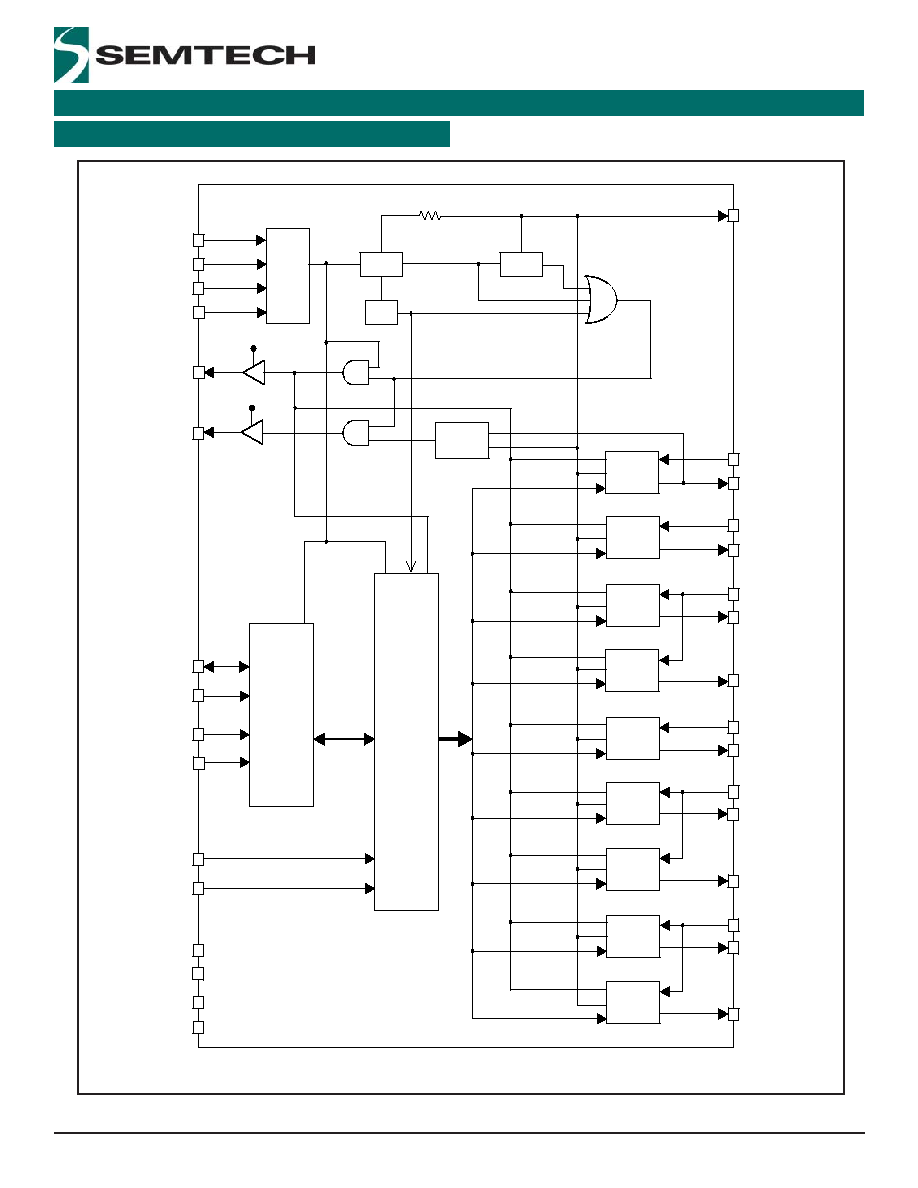
Block Diagram
VREF
OT
UVLO
RESET
VPAD
VPAD
PAD
EN
CORE
EN
CAM
EN
MOT
EN
ANA
EN
TCXO
EN
RX
EN
PLL
EN
TX
EN
EN
EN
REG
EN
CTRL
I
2
C Re
g
i
s
t
e
r
s
&
Co
n
t
r
o
l
I
2
C
In
te
r
f
a
c
e
BP
IN1
VPAD
IN2
VCORE
IN3
VCAM
VMOT
IN4
VANA
IN5
VTCXO
VRX
IN6
VPLL
VTX
AGND
DGND
SCL
SDA
VCSEL
VPSEL
EN_TCXO
EN_MOT
CHPWR
RESB
PWRON
PGOOD
HFPWR
ON
DVIN
VBAT
20
10
11
5
6
18
16
17
13
12
14
15
7
8
9
21
24
22
27
25
26
28
29
32
30
31
2
1
4
3
19
23
PWR
O
N
Logi
c

10
© 2006 Semtech Corp.
www.semtech.com
POWER MANAGEMENT
SC905A
any subsequent condition that toggles RESB (e.g. VPAD
short-circuit, over-temperature, under voltage lockout, I
2
C
disable of VPAD) will see a delay in the RESB transition
back to high of typically 250ms. The microprocessor then
raises PGOOD high to keep the SC905A powered on. There
is no time limit for the MSM to activate PGOOD. If the MSM
fails to raise PGOOD before the ON switch is released, the
SC905A will transition back into standby mode.
Once the phone is powered on, the SC905A can only be
directly powered off when the PGOOD signal goes low.
Therefore, if the ON pin transitions high when the PGOOD
signal is high, the LDOs and RESB signal will remain in their
state until the microprocessor pulls the PGOOD signal low.
Once the PGOOD signal is low, all the LDOs immediately
power off and all the logic resets to the shutdown condition.
The SC905A can be indirectly powered off by using the I
2
C
command to turn off the core supply. This will result in a
loss of power to the MSM causing PGOOD to go low, thus
disabling the SC905A.
The HFPWR and CHPWR pins operate identically to the ON
pin. These pins provide alternative sources for activating
power so that remote devices such as battery chargers or
system connector pins can be used to enable the device.
LDO Programmable Output Voltage
The output voltage of each LDO regulator is programmable.
Each LDO has a program voltage register that can be
accessed through the I
2
C interface and the output voltage
adjusted as necessary. (See the Tables on pages 14, 15
and 16 for more information.)
ON/OFF Control Register
Each individual LDO may be turned on or off by accessing
the ON/OFF control register. LDOs are turned on by setting
their respective on/off bits to 1 and disabled by setting the
on/off bits to 0. This allows for on/off control with a single
write command.
The register data is maintained when an on/off bit is
toggled, but all programmed information will be lost when
the PGOOD input goes low.
It should be noted that the enable signal control from the
I
2
C for LDOs TCXO and MOT are OR'd with their respective
external enable signals EN_TCXO and EN_MOT. This
General Description
The SC905A includes nine low dropout (LDO) voltage
regulators to provide complete power regulation capability for
CDMA handsets or other portable electronic equipment.
Five of the LDOs are designed to be used with analog
circuitry such as audio, radio frequency, or oscillator
circuits. These devices have very low noise levels and high
power supply rejection. The output voltage range for four of
these LDOs, VTCXO, VPLL, VTX and VRX, is 2.75V to 3.1V
in 50mV steps, and for the fi fth, VANA, the output voltage
range is 2.55V to 2.9V in 50mV steps. The TCXO LDO has
the additional feature of an external enable, EN_TCXO,
which can be used when timing is critical.
Two other LDOs are general purpose regulators designed
to be used with digital circuits. The noise requirements
for these LDOs are relaxed, but their voltage range is
expanded to cover the wide range of voltages needed for
different types of functions. The outputs for these LDOs
are VCORE and VPAD.
Two other LDOs are general purpose regulators that can be
used with other peripheral circuits. The VMOT and VCAM
outputs can be programmed to supply from 1.75V to 3.3V
in 50mV steps. The VMOT output is specifi cally designed
to drive a vibrator motor. This output can supply up to
150mA at any of the output voltage settings, allowing
designers the fl exibility to select the output voltage that
provides maximum vibration. The VMOT output also has
its own external enable, EN_MOT, to allow greater fl exibility.
When not used in conjunction with a vibrator, this output
can be used as a general purpose digital regulator. The
VCAM output is capable of supplying up to 100mA to drive
a digital camera module or any other peripheral circuit
found in a portable application.
Power-On Control
The SC905A is activated when the ON pin is pulled high,
provided that the input voltage is within the specifi ed
operating range. The ON pin responds to logic-high edge
triggering to power up the handset. The rising edge ON
signal is latched when the CORE, PAD, ANA, and TCXO LDOs
are turned on and PGOOD goes high. When the PAD LDO
output voltage reaches 77% of its regulation point, the reset
timer starts and the RESB signal transitions high after delay
of typically 100ms. After a successful power up sequence,
Applications Information

11
© 2006 Semtech Corp.
www.semtech.com
POWER MANAGEMENT
SC905A
means that these LDOs are on when there is a `1' in their
respective bit locations (register 6, bit 3 for VTCXO, register
2, bit 6 for VMOT), or if their external enable pins are pulled
HIGH. To turn these LDOs off the I
2
C on/off control bit
must be `0' and the external enable must be pulled LOW.
The state of EN_TCXO and EN_MOT can be established by
reading bits 0 and 2, respectively, in the Status Register.
VCSEL & VPSEL Pin
The VCSEL & VPSEL pins set the default voltage of CORE
and PAD LDOs respectively. When the VCSEL pin is set to
VIN
the default voltage for the CORE LDO is 1.80V. When
this pin is set to GND the default voltage for the CORE LDO
is 1.35V. Likewise, when the VPSEL pin is set to
VIN
the
default voltage for the PAD LDO is 3.00V. When this pin is
set to GND, the default voltage for the PAD LDO is 2.20V.
In both cases the VCSEL and VPSEL pins must be tied to
GND or
VIN
prior to the device being powered on. This
voltage cannot change on the fl y by switching the pin
voltage between VIN or GND once the device is on. The
voltage can be changed from its default state after start-up
by writing to the appropriate voltage code register.
Active Shutdown
The shutdown control bits determine how the on-chip
active shutdown switches behave. Register 7 is the
active shutdown control register and is used to control the
shutdown behavior. Each LDO has a specifi c shutdown
bit assigned to it. When the active shutdown bit is enabled
(set to 1), the output capacitance on the LDO output is
discharged by an on-chip FET when the LDO is disabled.
When the active shutdown bit is disabled (set to 0), the
output capacitance on the LDO output is discharged by
the load. The default state for each LDO
active shutdown
bit is on
.
Default Status Bit
In many multi-threaded environments it is necessary to
maintain synchronization between the host micro-controller
and the target IC. The SC905A has a default status bit
(DSB) that will facilitate this task. The DSB can be useful
in keeping the MSM and the SC905A synchronized.
However, this is only useful if the MSM is powered by an
external switching regulator such as Semtech's SC190A
switching regulator.
The DSB is bit 7 of register 0, and shares this register space
with the PAD voltage control bits. The DSB is only set to 1
during power-up to indicate that the part is set to the default
state. Moreover, the DSB cannot be written to a 1 through
the I
2
C interface the way the other bits in this register can;
it can only be cleared to 0 through the I
2
C interface. This
feature prevents a software race condition by always writing
to register 0 with bit 7 high when changing the PAD control
voltage. To clear the bit simply write a 0 to bit 7.
Applying the DSB
Upon power-up, the SC905A LDOs and internal registers are
set to their default state. The DSB is set to a 1 to indicate
that the SC905A is in its default state. Upon reading this
defaulted state condition, the MSM knows to perform
whatever synchronization is needed to set the SC905A
into a kno
wn
user state. This user state is entered by a
tw
o-sta
ge process.
1) The MSM writes a
0
to the DSB indicating its desire
to
modify
the state of the SC905A. It then writes all of the
correct register information to the SC905A to set it to the
user state.
2) The MSM reads back all of the information to verify the
data. Then it reads back the DSB again to ensure it is
still set to 0. This verifi es that no reset took place during
the time that the multiple writ
es
and re
ad
verifi cations
happened. If the DSB has been reset to 1, this process
needs to be repeated since the chip was reset sometime
during the initialization. Once the MSM and the SC905A
are synchronized, the DSB can be read back as a status
check periodically, as needed. If it is ever set back to the
default state, a new synchronization process is required.
This
handshake-style
protocol makes sure that the MSM
and SC905A are always synchronized.
LDO Power-On Sequence
When the SC905A fi rst turns on, the four LDOs that default
on are sequenced in the following fashio
n:
1) CORE, 2) PAD,
3) ANA, 4) TCXO. During the power-on sequenc
e, there is
a 200s delay between CORE and PAD to allow the output
of CORE to reach 1.2V before PAD is turned on, a delay of
100s between PAD and ANA turning on, and a delay of
100s between ANA and TCXO turning on. This process
eliminates large voltage spikes across the battery supply
during power-up. (For further information on LDO power
on sequen
cing, re
fer to the Timing Diagram on page 19.)
Applications Information (Cont.)

12
© 2006 Semtech Corp.
www.semtech.com
POWER MANAGEMENT
SC905A
Protection Circuitry
The SC905A
contains protection circuitry that prevents
the device from operating in an unspecifi ed state. These
include Under-voltage Lockout Protection, Over-temperature
Protection and Short-circuit Protection.
Under-Voltage Lockout
The SC905A provides an under-voltage lockout (UVLO)
circuit to protect the device from operating in an unknown
state if the input voltage supply is too low.
When the battery voltage drops below the UVLO threshold,
as defi ned in the Electrical Characteristics section, the
LDOs are disabled and RESB is held low. When the battery
voltage is increased above the hysteresis level, the LDOs
are re-enabled into their previous states, provided PGOOD
has remained high. If PGOOD goes low, the SC905A will
shut down. When powering-up with a battery voltage below
the UVLO threshold, RESB will be held low.
Over-Temperature Protection
The SC905A provides an internal over-temperature (OT)
protection circuit that monitors the internal junction
temperature. When the temperature exceeds the OT
threshold as defined in the Electrical Characteristics
section, the OT protection disables all the LDO outputs,
holds the RESB signal low and sets the OTF bit low in the
status register. When the junction temperature drops
below the hysteresis le
vel, t
he OT protection resets the OTF
bit high and re-enables all the LDOs in their previous states,
provided PGOOD has remained high. If PGOOD goes low,
the SC905A will shut down. This is only useful if the MSM
is not powered by the SC905A, since during an OT fault
the MSM will lose power. An external switching regulator
such as Semtech's SC190A could power the MSM in the
case where monitoring the OTF bit is desired.
Short-Circuit Protection
Each LDO output has short-circuit protection. If any output
is short-circuited to ground, the output voltage will drop
and the output current will be limited to the short circuit
current until the short is removed.
Status Register
The status register monitors the OTF and the state of the
external enable pins dedicated to the TCXO and MOT LDOs.
The MSM can periodically poll this register to determine
their status. This is a read-only register.
Applications Information (Cont.)
Layout Considerations
The
PCB
layout associated with the SC905A is
straightforward, with the main consideration being given
to the value and position of the input bypass capacitors.
The device has eight input voltage pins which can be
powered from a single supply or from a number of
individual supplies depending on how much copper is
available on the input voltage feed track and how much
real estate is available on the
PCB
for components.
If all the supply inputs are fed from one single supply
trace or from a power plane, a 10F low ESR capacitor
or two 4.7F low ESR capacitors should be used.
Larger input capacitance and lower ESR provide better
supply noise rejection and line transient response.
The copper trace to the inputs should be fairly thick in
order to keep trace inductance to a minimum and the
capacitors should be located as close to the SC905A
as possible. If the supply trace is thin then the inputs
should be treated as if they were powered from individual
supplies; each input should be bypassed by at least one
1F low ESR capacitor located very close to each input pin.
The SC905A is designed to have excellent stability
with a minimum output capacitance of 1F. Low ESR
ceramic capacitors are recommended and should be
located as close to the LDO output pins as possible.

13
© 2006 Semtech Corp.
www.semtech.com
POWER MANAGEMENT
SC905A
SC905A Slave Address:
Defaults are indicated in BOLD.
Notes:
(1) The default status bit (DSB) is set to 1 only when the SC905A is enabled by either the HFPWR pin or the ON pin being pulled high, and it
cannot be set to one through the I
2
C interface. When changing the VPAD control voltage, always write to register 0 with bit seven high. Set bit
seven low only when the DSB is to be cleared by the MSM. This will prevent any software race condition in a multi-tasking environment. See the
applications section for more information on using the DSB.
(2) The Active Shutdown defaults ON at power-up, but the registers maintain their settings as the LDOs are enabled and disabled during normal
operation.
DEVICE ADDRESS
R/W
0
0
0
1
0
0
0
X
Register Map
Register Name
Register
Address
Bit 7
Bit 6
Bit 5
Bit 4
Bit 3
Bit 2
Bit 1
Bit 0
Default
State
VPAD
VCORE
VMOT
VANA /VCAM
VTCXO/VRX
VPLL /VTX
ON/OFF
CONTROL
ACTIVE
(2 )
SHUTDOWN
STATUS
(READ ONLY)
0
1
2
3
4
6
5
7
8
DSB
(1 )
1
0
User
State
X
X
VPAD 4
VPAD 3
VPAD 2
VPAD 1
VPAD 0
X
X
X
VCORE4
VCORE3
VCORE2
VCORE1
VCORE0
X
VMOT_EN
VMOT
Active SHDN
VMOT4
VMOT3
VMOT2
VMOT1
VMOT0
1
0
1
0
OFF
OFF
ON
ON
VANA2
VANA1
VANA0
VCAM4
VCAM 3
VCAM2
VCAM1
VCAM 0
VTCXO2
VTCXO1
VTCXO0
VRX2
VRX1
VRX0
VPLL2
VPLL1
VPLL0
VTX2
VTX1
VTX0
X
X
X
X
VPAD _EN
1
0
OFF
ON
VCORE_EN
1
0
OFF
ON
VANA_EN
1
0
OFF
ON
VCAM_EN
1
0
OFF
ON
VTCXO_EN
1
0
OFF
ON
VPLL_EN
1
0
OFF
ON
VTX_EN
1
0
OFF
ON
VRX_EN
1
0
OFF
ON
VPAD
Active SHDN
1
0
OFF
ON
VCORE
Active SHDN
1
0
OFF
ON
VANA
Active SHDN
1
0
OFF
ON
VCAM
Active SHDN
1
0
OFF
ON
VTCXO
Active SHDN
1
0
OFF
ON
VPLL
Active SHDN
1
0
OFF
ON
VTX
Active SHDN
1
0
OFF
ON
VRX
Active SHDN
1
0
OFF
ON
EN_MOT
1
0
EN_TCXO
1
0
ON
OTF
1
0
OK
FAULT
X
X
X
X
OFF
ON
OFF
X
14
© 2006 Semtech Corp.
www.semtech.com
POWER MANAGEMENT
SC905A
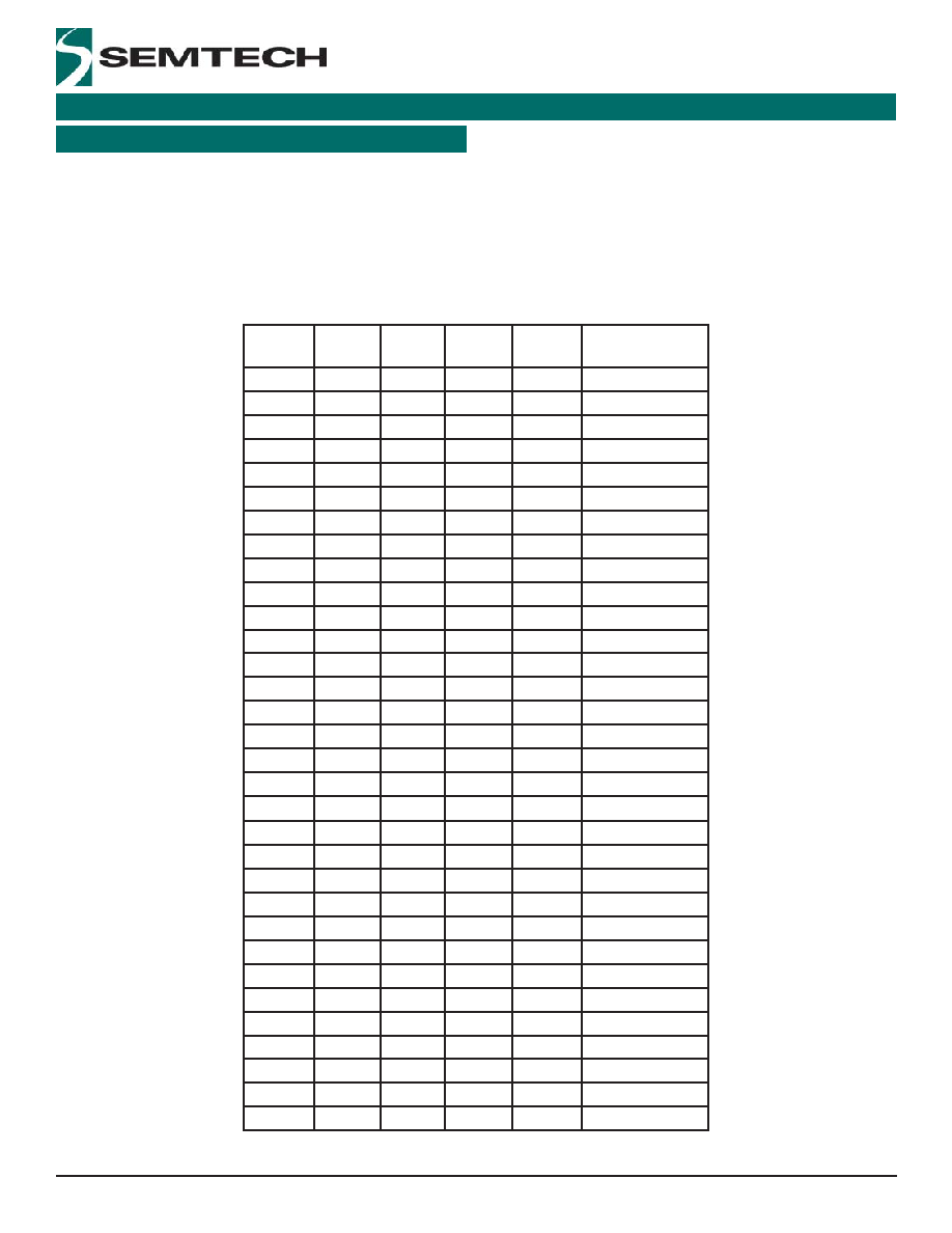
Digital LDO Voltage Tables A and B
A 5-bit linear DAC controls the output voltage of each LDO. The DAC and error-amp gain are scaled so that the LSB
size at the output is 50mV. Output voltage can be set by writing the proper code to the desired LDO register. See Table
A for the bitcodes and their corresponding voltages for LDO CORE, and Table B for bitcodes and their corresponding
voltages for LDOs PAD, MOT and CAM.
TABLE A - Output Voltage Code Bits for VCORE
X4
X3
X2
X1
X0
LDO Output
Voltage
0
0
0
0
0
1.35V
0
0
0
0
1
1.40V
0
0
0
1
0
1.45V
0
0
0
1
1
1.50V
0
0
1
0
0
1.55V
0
0
1
0
1
1.60V
0
0
1
1
0
1.65V
0
0
1
1
1
1.70V
0
1
0
0
0
1.75V
0
1
0
0
1
1.80V
0
1
0
1
0
1.85V
0
1
0
1
1
1.90V
0
1
1
0
0
1.95V
0
1
1
0
1
2.00V
0
1
1
1
0
2.05V
0
1
1
1
1
2.10V
1
0
0
0
0
2.15V
1
0
0
0
1
2.20V
1
0
0
1
0
2.25V
1
0
0
1
1
2.30V
1
0
1
0
0
2.35V
1
0
1
0
1
2.40V
1
0
1
1
0
2.45V
1
0
1
1
1
2.50V
1
1
0
0
0
2.55V
1
1
0
0
1
2.60V
1
1
0
1
0
2.65V
1
1
0
1
1
2.70V
1
1
1
0
0
2.75V
1
1
1
0
1
2.80V
1
1
1 1 0 2.85V
1
1
1
1
1
2.90V
Register Map (Cont.)

15
© 2006 Semtech Corp.
www.semtech.com
POWER MANAGEMENT
SC905A
TABLE B - Output Voltage Code Bits for VPAD, VMOT and VCAM
X4
X3
X2
X1
X0
LDO Output
Voltage
0
0
0
0
0
1.75V
0
0
0
0
1
1.80V
0
0
0
1
0
1.85V
0
0
0
1
1
1.90V
0
0
1
0
0
1.95V
0
0
1
0
1
2.00V
0
0
1
1
0
2.05V
0
0
1
1
1
2.10V
0
1
0
0
0
2.15V
0
1
0
0
1
2.20V
0
1
0
1
0
2.25V
0
1
0
1
1
2.30V
0
1
1
0
0
2.35V
0
1
1
0
1
2.40V
0
1
1
1
0
2.45V
0
1
1
1
1
2.50V
1
0
0
0
0
2.55V
1
0
0
0
1
2.60V
1
0
0
1
0
2.65V
1
0
0
1
1
2.70V
1
0
1
0
0
2.75V
1
0
1
0
1
2.80V
1
0
1
1
0
2.85V
1
0
1
1
1
2.90V
1
1
0
0
0
2.95V
1
1
0
0
1
3.00V
1
1
0
1
0
3.05V
1
1
0
1
1
3.10V
1
1
1
0
0
3.15V
1
1
1
0
1
3.20V
1
1
1 1 0 3.25V
1
1
1
1
1
3.30V
Register Map (Cont.)

16
© 2006 Semtech Corp.
www.semtech.com
POWER MANAGEMENT
SC905A
Analog LDO Voltage Tables C and D
The bit code controls the output voltage of each LDO. The LSB size at the output is 50mV. Output voltage can be set
by writing the proper code to the desired LDO register. See Table C for the bitcodes and their corresponding voltages
for LDO ANA, and Table D for the bitcodes and their corresponding voltages for LDOs TCXO, TX, RX and PLL.
TABLE C - Output Voltage Code Bits for LDO VANA
X2
X1
X0
LDO Output
Voltage
0
0
0
2.55V
0
0
1
2.60V
0
1
0
2.65V
0
1
1
2.70V
1
0
0
2.75V
1
0
1
2.80V
1
1
0
2.85V
1
1
1
2.90V
TABLE D - Output Voltage Code Bits for LDOs VTCXO, VTX, VRX, VPLL
X2
X1
X0
LDO Output
Voltage
0
0
0
2.75V
0
0
1
2.80V
0
1
0
2.85V
0
1
1
2.90V
1
0
0
2.95V
1
0
1
3.00V
1
1
0
3.05V
1
1
1
3.10V
Register Map (Cont.)
17
© 2006 Semtech Corp.
www.semtech.com
POWER MANAGEMENT
SC905A
The I
2
C General Specifi cation
The SC905A is a read-write slave-mode I
2
C device and complies with the Philips I
2
C standard Version 2.1 dated January,
2000. The SC905A has eight user-accessible internal 8-bit registers. The I
2
C interface has been designed for program
fl exibility, in that once the slave address has been sent to the SC905A enabling it to be a slave transmitter/receiver, any
register can be written or read independently of each other. While there is no auto increment/decrement capability in
the SC905A I
2
C logic, a tight software loop can be designed to randomly access the next register independent of which
register you begin accessing. The start and stop commands frame the data-packet and the repeat start condition is
allowed if necessary.
SC905A Limitations to the I
2
C Specifi cations
Seven bit addressing is used and ten bit addressing is not allowed. Any general call address will be ignored by the
SC905A. The SC905A is not CBUS compatible. The SC905A can operate in standard mode (100kbit/s) or fast mode
(400kbit/s).
Supported Formats
Direct Format - Write
The simplest format for an I
2
C write is given below. After the start condition [S], the slave address is sent, followed
by an eighth bit indicating a write. The SC905A I
2
C then acknowledges that it is being addressed, and the master
responds with an 8-bit data byte consisting of the register address. The slave acknowledges and the master sends
the appropriate 8-bit data byte. Once again the slave acknowledges and the master terminates the transfer with the
stop condition [P].
Combined Format - Read
After the start condition [S], the slave address is sent, followed by an eighth bit indicating a write. The SC905A I
2
C then
acknowledges that it is being addressed, and the master responds with an 8-bit data byte consisting of the register
address. The slave acknowledges and the master sends the repeated start condition [Sr]. Once again, the slave
address is sent, followed by an eighth bit indicating a read. The slave responds with an acknowledge and the previously
addressed 8-bit data byte; the master then sends a non-acknowledge (NACK). Finally, the master terminates the
transfer with the stop condition [P].
Slave Address
Register Address
Data
S
W A
A
A P
S: Start Condition
Slave Address: 7-bit
W: Write = `0'
Register Address: 8-bit
A: Acknowledge (sent by slave)
Data: 8-bit
P: Stop condition
I
2
C Direct Format - Write
Using the I
2
C Serial Port
Slave Address
Register Address
Slave Address
Data
NACK
S
W A
A Sr
R A
P
S: Start Condition
Slave Address: 7-bit
W: Write = `0'
Register Address: 8-bit
R: Read = `1'
Data: 8-bit
A: Acknowledge (sent by slave)
NACK: Non-Acknowledge (sent by master)
Sr: Repeated Start Condition
P: Stop condition
I
2
C Combined Format - Read

18
© 2006 Semtech Corp.
www.semtech.com
POWER MANAGEMENT
SC905A
Stop-Separated Reads
Stop-separated reads can also be used. This format allows a master to set up the register address pointer for a read
and return to that slave at a later time to read the data. In this format the slave address followed by a write command
are sent after a start [S] condition. The SC905A then acknowledges it is being addressed, and the master responds
with the 8-bit register address. The master sends a stop or restart condition and may then address another slave. After
performing other tasks, the master can send a start or restart condition to the SC905A with a read command. The
SC905A acknowledges this request and returns the data from the register location that had previously been set up
.
Slave Address
Register Address
Slave Address B
Data
NACK
S
W A
A
S/Sr
R A
P
P
Slave Address A
S
S: Start Condition
Slave Address: 7-bit
W: Write = `0'
Register Address: 8-bit
R: Read = `1'
Data: 8-bit
A: Acknowledge (sent by slave)
NACK: Non-Acknowledge (sent by master)
Sr: Repeated Start Condition
P: Stop condition
I
2
C Stop Separated Format - Read
Register Address Setup Access
Master Addresses
other Slaves
Register Read Access
Using the I
2
C Serial Port (Cont.)
19
© 2006 Semtech Corp.
www.semtech.com
POWER MANAGEMENT
SC905A
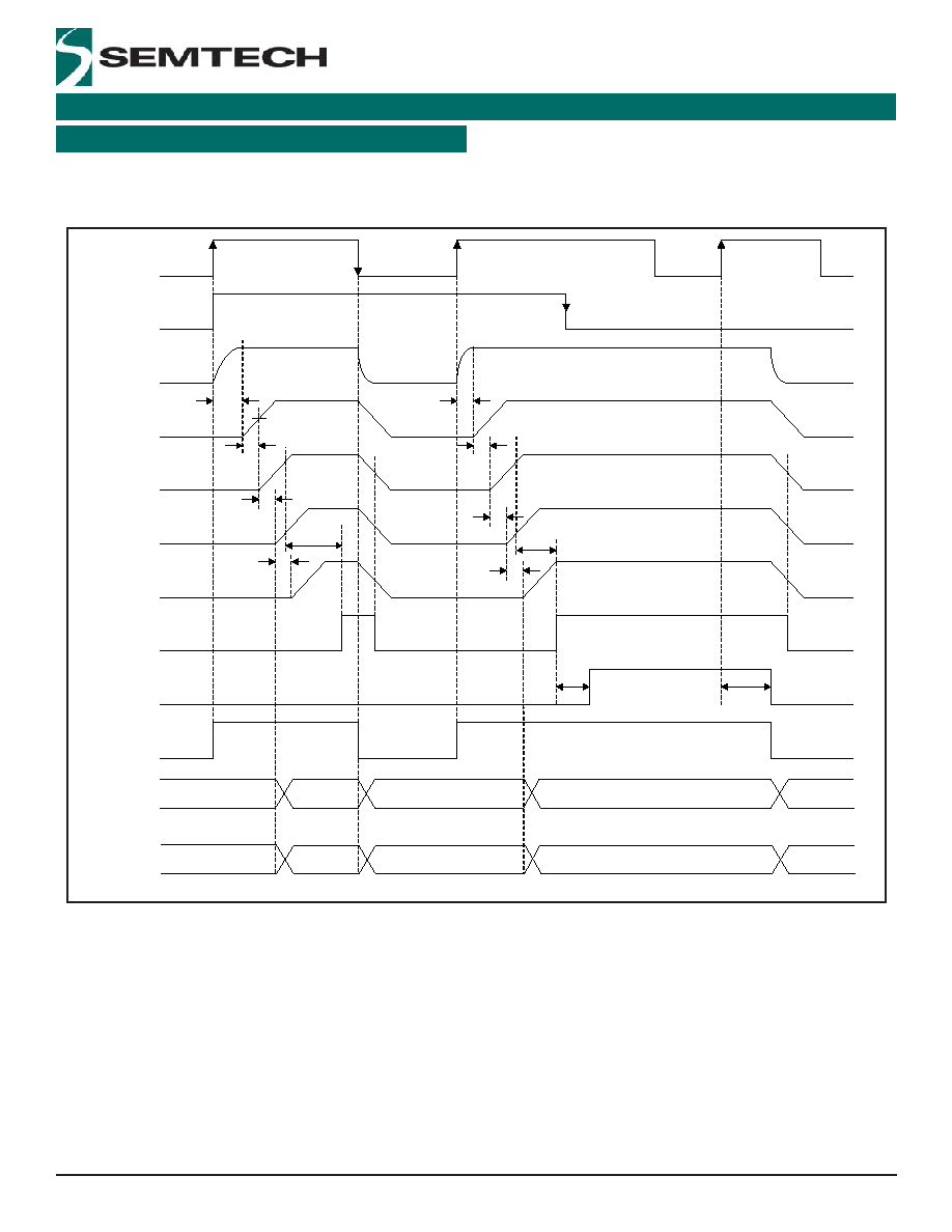
Timing Diagram
Power On-Off Timing Diagram
77%
77%
77%
77%
25ms
200s
100s
100s
100ms
100s
100s
100s
100ms
25ms
MSM
DETERMINED
MSM
DETERMINED
ON, HFPWR
or
CHPWR
DSB
BP
VCORE
VPAD
VANA
VTCXO
RESB
PGOOD
PWRON
MSM
DETERMINED
1.2V
EN_TCXO
EN_MOT
XXXXXXXXXX
XXXX
XXXXXXXX
XXXXXXXXXX
XXXX
XXXXXXXX

20
© 2006 Semtech Corp.
www.semtech.com
POWER MANAGEMENT
SC905A
0
25
50
75
100
125
150
175
200
80
100
120
140
160
180
200
0
25
50
75
100
125
150
175
200
225
100
125
150
175
200
225
250
275
300
-18
-15
-12
-9
-6
-3
0
0
25
50
75
100
125
150
175
200
-15
-12
-9
-6
-3
0
0
50
100
150
200
250
300
0
1
2
3
4
5
3
3.5
4
4.5
5
5.5
0
1
2
3
4
5
6
3
3.5
4
4.5
5
5.5
T = -40∞C
T = -40∞C
T = -40∞C
T = -40∞C
T = -40∞C
T = -40∞C
T = 25∞C
T = 25∞C
T = 25∞C
T = 25∞C
T = 25∞C
T = 25∞C
T = 85∞C
T = 85∞C
T = 85∞C
T = 85∞C
T = 85∞C
T = 85∞C
Typical Characteristics
Input Voltage (V)
Input Voltage (V)
Load Current (mA)
Load Current (mA)
Load Current (mA)
Load Current (mA)
Dropout V
oltage (mV)
Dropout V
oltage (mV)
Output V
oltage V
ariation (mV)
Output V
oltage V
ariation (mV)
Output V
oltage V
ariation (mV)
Output V
oltage V
ariation (mV)
Dropout Voltage vs. Load Current (Analog LDOs)
Dropout Voltage vs. Load Current (Digital LDOs)
Load Regulation (Analog LDOs) V
IN
= 3.7V
Load Regulation (Digital LDOs) V
IN
= 3.7V
Line Regulation (Analog LDOs) I
LOAD
= 1mA
Line Regulation (Digital LDOs) I
LOAD
= 1mA

21
© 2006 Semtech Corp.
www.semtech.com
POWER MANAGEMENT
SC905A
Typical Characteristics (Cont.)
0
0.2
0.4
0.6
0.8
1
1.2
1.4
1.6
2.7
3.1
3.5
3.9
4.3
4.7
5.1
5.5
5.9
-90
-80
-70
-60
-50
-40
-30
-20
-10
0
10
100
1000
10000
-80
-70
-60
-50
-40
-30
-20
-10
0
10
100
1000
10000
0
5
10
15
20
25
30
35
40
45
0
25
50
75
100
125
150
175
200
T = 85∞C
T = 25∞C
T = -40∞C
V
OUT
= 1.35V
V
OUT
= 2.90V
Frequency (Hz)
Frequency (Hz)
Input Voltage (V)
Load Current (mA)
Power Supply Rejection (dB)
Power Supply Rejection (dB)
Maximum Outptu Current (A)
Output Noise (
V)
PSRR vs. Frequency (Analog LDOs)
V
OUT
= V
OUT(MAX)
, V
IN
= 3.7V, I
LOAD
= 50mA
Safe Operating Limits
Output Noise vs. Load Current (Analog LDOs)
V
OUT
= V
OUT(MAX)
, V
IN
= 3.7V
PSRR vs. Frequency (Digital LDOs)
V
OUT
= V
OUT(MAX)
, V
IN
= 3.7V, I
LOAD
= 50mA

22
© 2006 Semtech Corp.
www.semtech.com
POWER MANAGEMENT
SC905A
Outline Drawing - MLPQ-32 5x5
e
MILLIMETERS
0.50 BSC
.002
-
0.00
.000
A1
.193
.193
.130
.130
.012
.007
E1
aaa
bbb
N
e
L
A2
D1
D
E
b
.020 BSC
.136
.016
.003
.004
32
.197
(.008)
.136
.197
.010
-
3.30
.140
.020 0.30
.201
.201
.140
-
.012
4.90
4.90
3.30
-
0.18
.031
MIN
DIM
A
MAX
DIMENSIONS
INCHES
-
NOM
.039 0.80
MIN
-
0.05
5.10
5.10
3.55
3.55
0.50
0.30
3.45
0.40
0.10
0.08
32
5.00
(0.20)
3.45
5.00
0.25
-
1.00
MAX
-
NOM
B
aaa C
C
SEATING
PLANE
1
2
N
bbb
C A B
COPLANARITY APPLIES TO THE EXPOSED PAD AS WELL AS THE TERMINALS.
CONTROLLING DIMENSIONS ARE IN MILLIMETERS (ANGLES IN DEGREES).
NOTES:
2.
1.
A
PIN 1
INDICATOR
(LASER MARK)
D
E
E/2
LxN
A2
E1
bxN
D/2
A
A1
D1

23
© 2006 Semtech Corp.
www.semtech.com
POWER MANAGEMENT
SC905A
Land Pattern - MLPQ-32 5x5
2x (C)
2x G
2x Z
Y TYP
P
TYP
X
TYP
K
H
THIS LAND PATTERN IS FOR REFERENCE PURPOSES ONLY.
CONSULT YOUR MANUFACTURING GROUP TO ENSURE YOUR
NOTES:
1.
DIM
X
Y
H
K
P
C
G
MILLIMETERS
INCHES
(5.00)
.012
.031
.165
.021
.146
.146
(.197)
0.30
0.80
3.70
0.50
3.70
4.20
DIMENSIONS
COMPANY'S MANUFACTURING GUIDELINES ARE MET.
5.80
.228
Z
Semtech Corporation
Power Management Products Division
200 Flynn Road, Camarillo, CA 93012
Phone: (805) 498-2111 FAX (805)498-3804
Contact Information