1
www.semtech.com
PROTECTION PRODUCTS
SR05
RailClamp
Low Capacitance TVS Diode Array
Description
Features
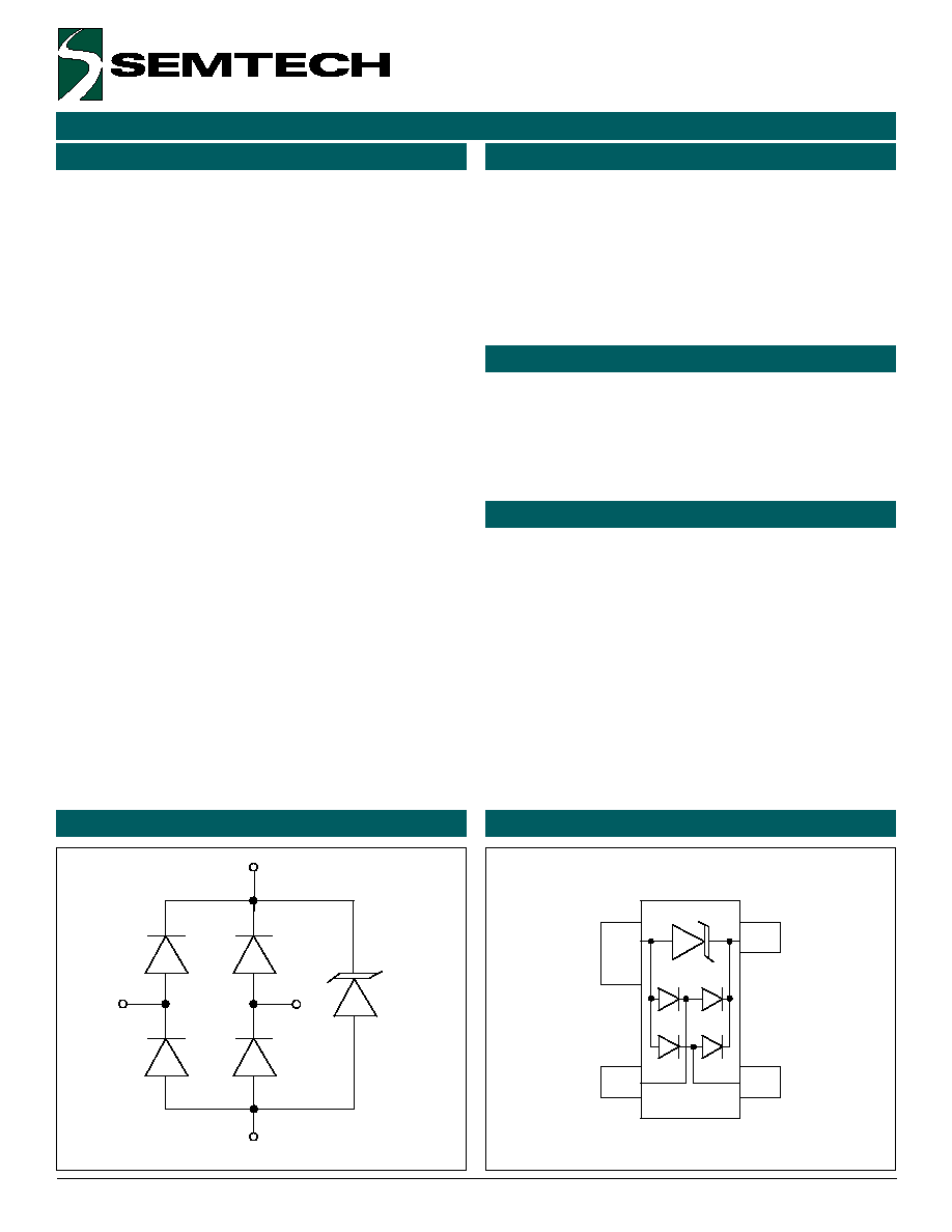
Circuit Diagram
Schematic & PIN Configuration
Revision 9/2000
RailClamps are surge rated diode arrays designed to
protect high speed data interfaces. The SR series has
been specifically designed to protect sensitive compo-
nents which are connected to data and transmission
lines from overvoltage caused by ESD (electrostatic
discharge), EFT (electrical fast transients), and light-
ning.
The unique design of the SR series devices incorpo-
rates four surge rated, low capacitance steering diodes
and a TVS diode in a single package. During transient
conditions, the steering diodes direct the transient to
either the positive side of the power supply line or to
ground. The internal TVS diode prevents over-voltage
on the power line, protecting any downstream compo-
nents.
The low capacitance array configuration allows the user
to protect two high-speed data or transmission lines.
The low inductance construction minimizes voltage
overshoot during high current surges.
Applications
Mechanical Characteristics
!
USB Power & Data Line Protection
!
Ethernet 10BaseT
!
I
2
C Bus Protection
!
Video Line Protection
!
T1/E1 secondary IC Side Protection
!
Portable Electronics
!
Microcontroller Input Protection
!
WAN/LAN Equipment
!
ISDN S/T Interface
!
ESD protection to IEC 61000-4-2, Level 4
!
Array of surge rated diodes with internal TVS Diode
!
Protects two I/O lines
!
Low capacitance (<10pF) for high-speed interfaces
!
Low clamping voltage
!
Low operating voltage: 5.0V
!
Solid-state silicon-avalanche technology
!
JEDEC SOT-143 package
!
UL 497B listed
!
Molding compound flammability rating: UL 94V-0
!
Marking : R05
!
Packaging : Tape and Reel per EIA 481
Pin 4
Pin 2
Pin 3
Pin 1
SOT-143 (Top View)
1
2
3
4

2
2000 Semtech Corp.
www.semtech.com
PROTECTION PRODUCTS
SR05
Absolute Maximum Rating
Electrical Characteristics
5
0
R
S
r
e
t
e
m
a
r
a
P
l
o
b
m
y
S
s
n
o
i
t
i
d
n
o
C
m
u
m
i
n
i
M
l
a
c
i
p
y
T
m
u
m
i
x
a
M
s
t
i
n
U
e
g
a
tl
o
V
f
f
O
-
d
n
a
t
S
e
s
r
e
v
e
R
V
M
W
R
5
V
e
g
a
tl
o
V
n
w
o
d
k
a
e
r
B
e
s
r
e
v
e
R
V
R
B
I
t
A
m
1
=
6
V
t
n
e
r
r
u
C
e
g
a
k
a
e
L
e
s
r
e
v
e
R
I
R
V
M
W
R
C
�
5
2
=
T
,
V
5
=
5
A
�
e
g
a
tl
o
V
g
n
i
p
m
a
l
C
V
C
I
P
P
s
�
0
2
/
8
=
p
t
,
A
1
=
8
.
9
V
e
g
a
tl
o
V
g
n
i
p
m
a
l
C
V
C
I
P
P
s
�
0
2
/
8
=
p
t
,
A
0
1
=
2
1
V
e
g
a
tl
o
V
g
n
i
p
m
a
l
C
V
C
I
P
P
s
�
0
2
/
8
=
p
t
,
A
5
2
=
0
2
V
e
c
n
a
ti
c
a
p
a
C
n
o
it
c
n
u
J
C
j
d
n
a
s
n
i
p
O
/
I
n
e
e
w
t
e
B
d
n
G
V
R
z
H
M
1
=
f
,
V
0
=
6
0
1
F
p
s
n
i
p
O
/
I
n
e
e
w
t
e
B
V
R
z
H
M
1
=
f
,
V
0
=
3
F
p
g
n
i
t
a
R
l
o
b
m
y
S
e
u
l
a
V
s
t
i
n
U
)
s
�
0
2
/
8
=
p
t
(
r
e
w
o
P
e
s
l
u
P
k
a
e
P
P
k
p
0
0
5
s
t
t
a
W
)
s
�
0
2
/
8
=
p
t
(
t
n
e
r
r
u
C
e
s
l
u
P
k
a
e
P
I
P
P
5
2
A
I(
e
g
a
tl
o
V
d
r
a
w
r
o
F
k
a
e
P
F
)
s
�
0
2
/
8
=
p
t
,
A
1
=
V
P
F
5
.
1
V
e
r
u
t
a
r
e
p
m
e
T
g
n
ir
e
d
l
o
S
d
a
e
L
T
L
).
c
e
s
0
1
(
0
6
2
C
�
e
r
u
t
a
r
e
p
m
e
T
g
n
it
a
r
e
p
O
T
J
5
2
1
+
o
t
5
5
-
C
�
e
r
u
t
a
r
e
p
m
e
T
e
g
a
r
o
t
S
T
G
T
S
0
5
1
+
o
t
5
5
-
C
�
3
2000 Semtech Corp.
www.semtech.com
PROTECTION PRODUCTS
SR05
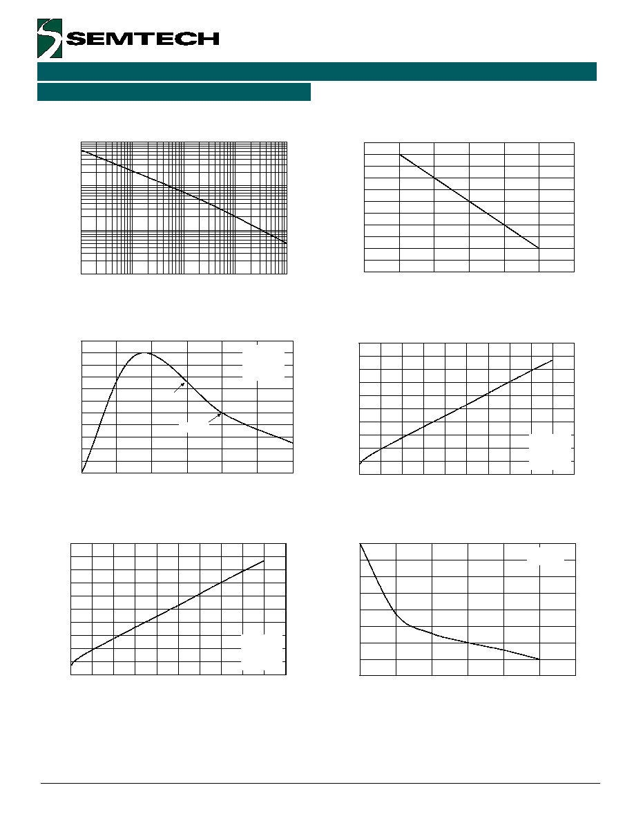
Typical Characteristics
Non-Repetitive Peak Pulse Power vs. Pulse Time
Power Derating Curve
0.01
0.1
1
10
0.1
1
10
100
1000
Pulse Duration - tp (
�
�
�
�
s)
Peak Pulse Power - P
PP
(kW)
0
10
20
30
40
50
60
70
80
90
100
110
0
25
50
75
100
125
150
Ambient Temperature - T
A
(
o
C)
% of Rated Power or I
PP
Clamping Voltage vs. Peak Pulse Current
0
10
20
30
40
50
60
70
80
90
100
110
0
5
10
15
20
25
30
Time (
�
�
�
�
s)
Percent of I
PP
e
-t
td = I
PP
/2
Waveform
Parameters:
tr = 8
�
s
td = 20
�
s
Pulse Waveform
0
1
2
3
4
5
6
7
8
9
10
0
5
10
15
20
25
30
35
40
45
50
Forward Current - I
F
(A)
Forward Voltage - V
F
(V)
Waveform
Parameters:
tr = 8
�
s
td = 20
�
s
Forward Voltage vs. Forward Current
Capacitance vs. Reverse Voltage
0
1
2
3
4
5
6
7
8
9
10
0
5
10
15
20
25
30
35
40
45
50
Forward Current - I
F
(A)
Forward Voltage - V
F
(V)
Waveform
Parameters:
tr = 8
�
s
td = 20
�
s
-16
-14
-12
-10
-8
-6
-4
-2
0
0
1
2
3
4
5
6
Reverse Voltage (V)
% Change in Capacitanc
e
I/O to GND
f = 1MHz
4
2000 Semtech Corp.
www.semtech.com
PROTECTION PRODUCTS
SR05
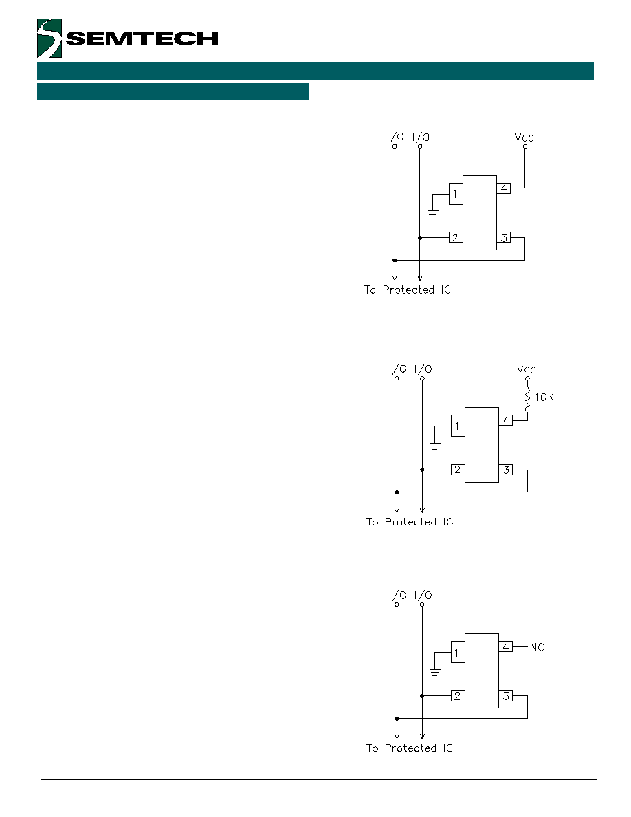
Device Connection Options for Protection of Two
High-Speed Data Lines
The SR05 TVS is designed to protect two data lines
from transient over-voltages by clamping them to a
fixed reference. When the voltage on the protected
line exceeds the reference voltage (plus diode V
F
) the
steering diodes are forward biased, conducting the
transient current away from the sensitive circuitry.
Data lines are connected at pins 2 and 3. The nega-
tive reference (REF1) is connected at pin 1. This pin
should be connected directly to a ground plane on the
board for best results. The path length is kept as short
as possible to minimize parasitic inductance.
The positive reference (REF2) is connected at pin 4.
The options for connecting the positive reference are
as follows:
1. To protect data lines and the power line, connect
pin 4 directly to the positive supply rail (V
CC
). In this
configuration the data lines are referenced to the
supply voltage. The internal TVS diode prevents
over-voltage on the supply rail.
2. The SR05 can be isolated from the power supply by
adding a series resistor between pin 4 and V
CC
. A
value of 10k
is recommended. The internal TVS
and steering diodes remain biased, providing the
advantage of lower capacitance.
3. In applications where no positive supply reference
is available, or complete supply isolation is desired,
the internal TVS may be used as the reference. In
this case, pin 4 is not connected. The steering
diodes will begin to conduct when the voltage on
the protected line exceeds the working voltage of
the TVS (plus one diode drop).
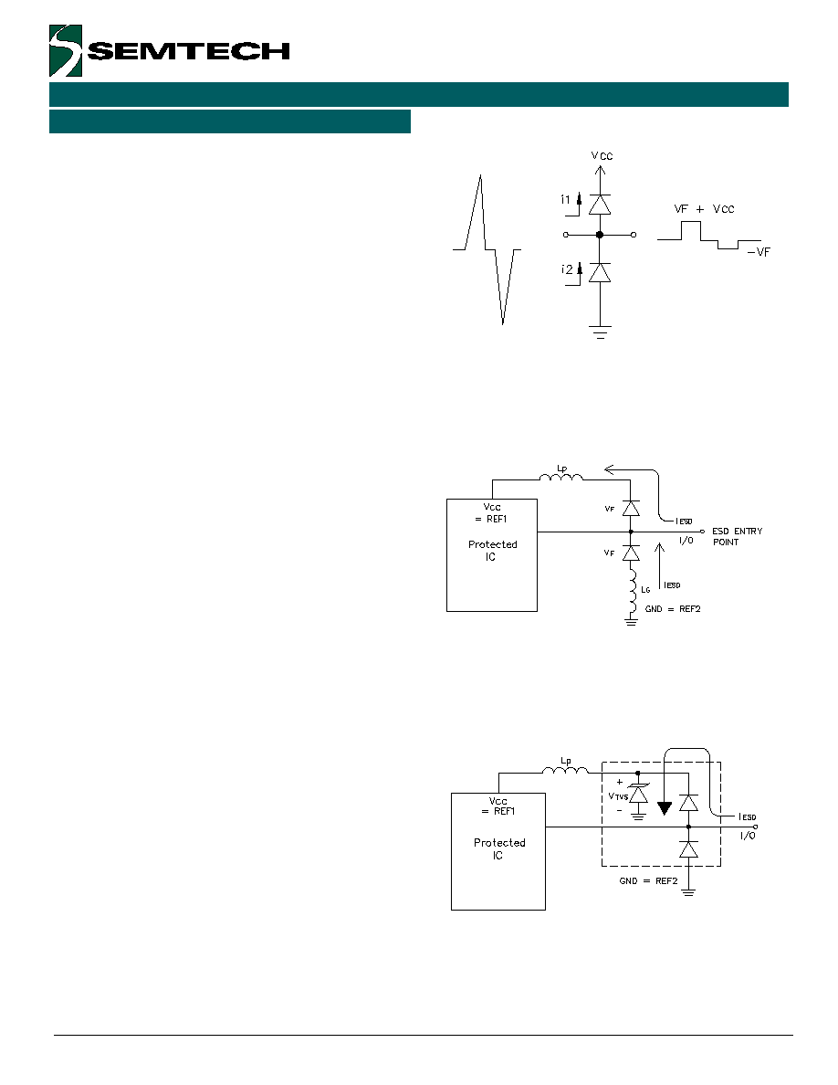
ESD Protection With RailClamps
RailClamps are optimized for ESD protection using the
rail-to-rail topology. Along with good board layout,
these devices virtually eliminate the disadvantages of
using discrete components to implement this topology.
Consider the situation shown in Figure 1 where dis-
crete diodes or diode arrays are configured for rail-to-
rail protection on a high speed line. During positive
duration ESD events, the top diode will be forward
biased when the voltage on the protected line exceeds
the reference voltage plus the V
F
drop of the diode.
Data Line and Power Supply Protection Using Vcc as
reference
Data Line Protection with Bias and Power Supply
Isolation Resistor
Data Line Protection Using Internal TVS Diode as
Reference
Applications Information
5
2000 Semtech Corp.
www.semtech.com
PROTECTION PRODUCTS
SR05
PIN Descriptions
For negative events, the bottom diode will be biased
when the voltage exceeds the V
F
of the diode. At first
approximation, the clamping voltage due to the charac-
teristics of the protection diodes is given by:
V
C
= V
CC
+ V
F
(for positive duration pulses)
V
C
= -V
F
(for negative duration pulses)
However, for fast rise time transient events, the
effects of parasitic inductance must also be consid-
ered as shown in Figure 2. Therefore, the actual
clamping voltage seen by the protected circuit will be:
V
C
= V
CC
+ V
F
+ L
P
di
ESD
/dt (for positive duration pulses)
V
C
= -V
F
- L
G
di
ESD
/dt
(for negative duration pulses)
ESD current reaches a peak amplitude of 30A in 1ns
for a level 4 ESD contact discharge per IEC 1000-4-2.
Therefore, the voltage overshoot due to 1nH of series
inductance is:
V = L
P
di
ESD
/dt = 1X10
-9
(30 / 1X10
-9
) = 30V
Example:
Consider a V
CC
= 5V, a typical V
F
of 30V (at 30A) for the
steering diode and a series trace inductance of 10nH.
The clamping voltage seen by the protected IC for a
positive 8kV (30A) ESD pulse will be:
V
C
= 5V + 30V + (10nH X 30V/nH) = 335V
This does not take into account that the ESD current is
directed into the supply rail, potentially damaging any
components that are attached to that rail. Also note
that it is not uncommon for the V
F
of discrete diodes to
exceed the damage threshold of the protected IC. This
is due to the relatively small junction area of typical
discrete components. It is also possible that the
power dissipation capability of the discrete diode will
be exceeded, thus destroying the device.
The RailClamp is designed to overcome the inherent
disadvantages of using discrete signal diodes for ESD
suppression. The RailClamp's integrated TVS diode
helps to mitigate the effects of parasitic inductance in
Figure 1 - "Rail-
Figure 1 - "Rail-
Figure 1 - "Rail-
Figure 1 - "Rail-
Figure 1 - "Rail-TTTTTo-Rail" Pr
o-Rail" Pr
o-Rail" Pr
o-Rail" Pr
o-Rail" Proooootttttection T
ection T
ection T
ection T
ection Topology
opology
opology
opology
opology
(First Approximation)
(First Approximation)
(First Approximation)
(First Approximation)
(First Approximation)
Figure 2 - The Effects of Parasitic Inductance
Figure 2 - The Effects of Parasitic Inductance
Figure 2 - The Effects of Parasitic Inductance
Figure 2 - The Effects of Parasitic Inductance
Figure 2 - The Effects of Parasitic Inductance
When Using Discrete Components to Implement
When Using Discrete Components to Implement
When Using Discrete Components to Implement
When Using Discrete Components to Implement
When Using Discrete Components to Implement
Rail-
Rail-
Rail-
Rail-
Rail-TTTTTo-Rail Pr
o-Rail Pr
o-Rail Pr
o-Rail Pr
o-Rail Proooootttttection
ection
ection
ection
ection
Figure 3 - Rail-
Figure 3 - Rail-
Figure 3 - Rail-
Figure 3 - Rail-
Figure 3 - Rail-TTTTTo-Rail Pr
o-Rail Pr
o-Rail Pr
o-Rail Pr
o-Rail Proooootttttection Using
ection Using
ection Using
ection Using
ection Using
RailClam
RailClam
RailClam
RailClam
RailClamp T
p T
p T
p T
p T VVVVVS Arra
S Arra
S Arra
S Arra
S Arrays
ys
ys
ys
ys
Applications Information (continued)