1
www.semtech.com
PROTECTION PRODUCTS
SR3.3
RailClamp
Low Capacitance TVS Diode Array
PRELIMINARY
Description
Features
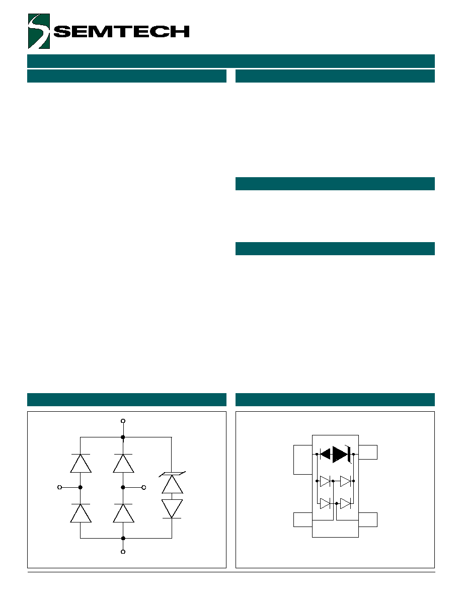
Circuit Diagram
Schematic & PIN Configuration
Revision 9/2000
RailClamps are surge rated diode arrays designed to
protect high speed data interfaces. The SR series has
been specifically designed to protect sensitive compo-
nents which are connected to data and transmission
lines from overvoltage caused by ESD (electrostatic
discharge), EFT (electrical fast transients), and tertiary
lightning.
The unique design of the SR series devices incorpo-
rates four surge rated, low capacitance steering diodes
and a TVS diode in a single package. The TVS diode is
constructed using Semtech's proprietary low voltage
EPD technology for superior electrical characteristics at
3.3 volts.
During transient conditions, the steering diodes direct
the transient to either the positive side of the power
supply line or to ground. The internal TVS diode pre-
vents over-voltage on the power line, protecting any
downstream components.
The low capacitance array configuration allows the user
to protect two high-speed data or transmission lines.
The low inductance construction minimizes voltage
overshoot during high current surges.
Applications
Mechanical Characteristics
!
Data and I/O lines
!
Sensitive Analog Inputs
!
Video Line Protection
!
Portable Electronics
!
Microcontroller Input Protection
!
WAN/LAN Equipment
!
ESD protection to IEC 61000-4-2, Level 4
!
Array of surge rated diodes with internal
EPD TVS
diode
!
Protects two I/O lines
!
Low capacitance (<10pF) for high-speed interfaces
!
Low leakage current (< 1�A)
!
Low operating voltage: 3.3V
!
Solid-state technology
!
JEDEC SOT-143 package
!
Molding compound flammability rating: UL 94V-0
!
Marking : R3.3
!
Packaging : Tape and Reel per EIA 481
Pin 4
Pin 2
Pin 3
Pin 1
1
2
3
4
SOT-143 (Top View)

2
2000 Semtech Corp.
www.semtech.com
PROTECTION PRODUCTS
SR3.3
PRELIMINARY
Absolute Maximum Rating
Electrical Characteristics
3
.
3
R
S
r
e
t
e
m
a
r
a
P
l
o
b
m
y
S
s
n
o
i
t
i
d
n
o
C
m
u
m
i
n
i
M
l
a
c
i
p
y
T
m
u
m
i
x
a
M
s
t
i
n
U
e
g
a
t
l
o
V
f
f
O
-
d
n
a
t
S
e
s
r
e
v
e
R
V
M
W
R
3
.
3
V
e
g
a
t
l
o
V
h
g
u
o
r
h
T
-
h
c
n
u
P
V
T
P
I
T
P
A
�
2
=
5
.
3
V
e
g
a
t
l
o
V
k
c
a
B
-
p
a
n
S
V
B
S
I
B
S
A
m
0
5
=
8
.
2
V
t
n
e
r
r
u
C
e
g
a
k
a
e
L
e
s
r
e
v
e
R
I
R
V
M
W
R
C
�
5
2
=
T
,
V
3
.
3
=
1
A
�
e
g
a
t
l
o
V
g
n
i
p
m
a
l
C
V
C
I
P
P
s
�
0
2
/
8
=
p
t
,
A
1
=
7
V
e
g
a
t
l
o
V
g
n
i
p
m
a
l
C
V
C
I
P
P
s
�
0
2
/
8
=
p
t
,
A
0
1
=
5
1
V
t
n
e
r
r
u
C
e
s
l
u
P
k
a
e
P
m
u
m
i
x
a
M
I
P
P
s
�
0
2
/
8
=
p
t
0
1
A
e
c
n
a
t
i
c
a
p
a
C
n
o
i
t
c
n
u
J
C
j
d
n
a
s
n
i
p
O
/
I
n
e
e
w
t
e
B
d
n
G
V
R
z
H
M
1
=
f
,
V
0
=
6
0
1
F
p
s
n
i
p
O
/
I
n
e
e
w
t
e
B
V
R
z
H
M
1
=
f
,
V
0
=
3
F
p
g
n
i
t
a
R
l
o
b
m
y
S
e
u
l
a
V
s
t
i
n
U
)
s
�
0
2
/
8
=
p
t
(
r
e
w
o
P
e
s
l
u
P
k
a
e
P
P
k
p
0
5
1
s
t
t
a
W
)
s
�
0
2
/
8
=
p
t
(
t
n
e
r
r
u
C
e
s
l
u
P
k
a
e
P
I
P
P
0
1
A
I(
e
g
a
tl
o
V
d
r
a
w
r
o
F
k
a
e
P
F
)
s
�
0
2
/
8
=
p
t
,
A
1
=
V
P
F
5
.
1
V
e
r
u
t
a
r
e
p
m
e
T
g
n
ir
e
d
l
o
S
d
a
e
L
T
L
).
c
e
s
0
1
(
0
6
2
C
�
e
r
u
t
a
r
e
p
m
e
T
g
n
it
a
r
e
p
O
T
J
5
2
1
+
o
t
5
5
-
C
�
e
r
u
t
a
r
e
p
m
e
T
e
g
a
r
o
t
S
T
G
T
S
0
5
1
+
o
t
5
5
-
C
�
3
2000 Semtech Corp.
www.semtech.com
PROTECTION PRODUCTS
SR3.3
PRELIMINARY
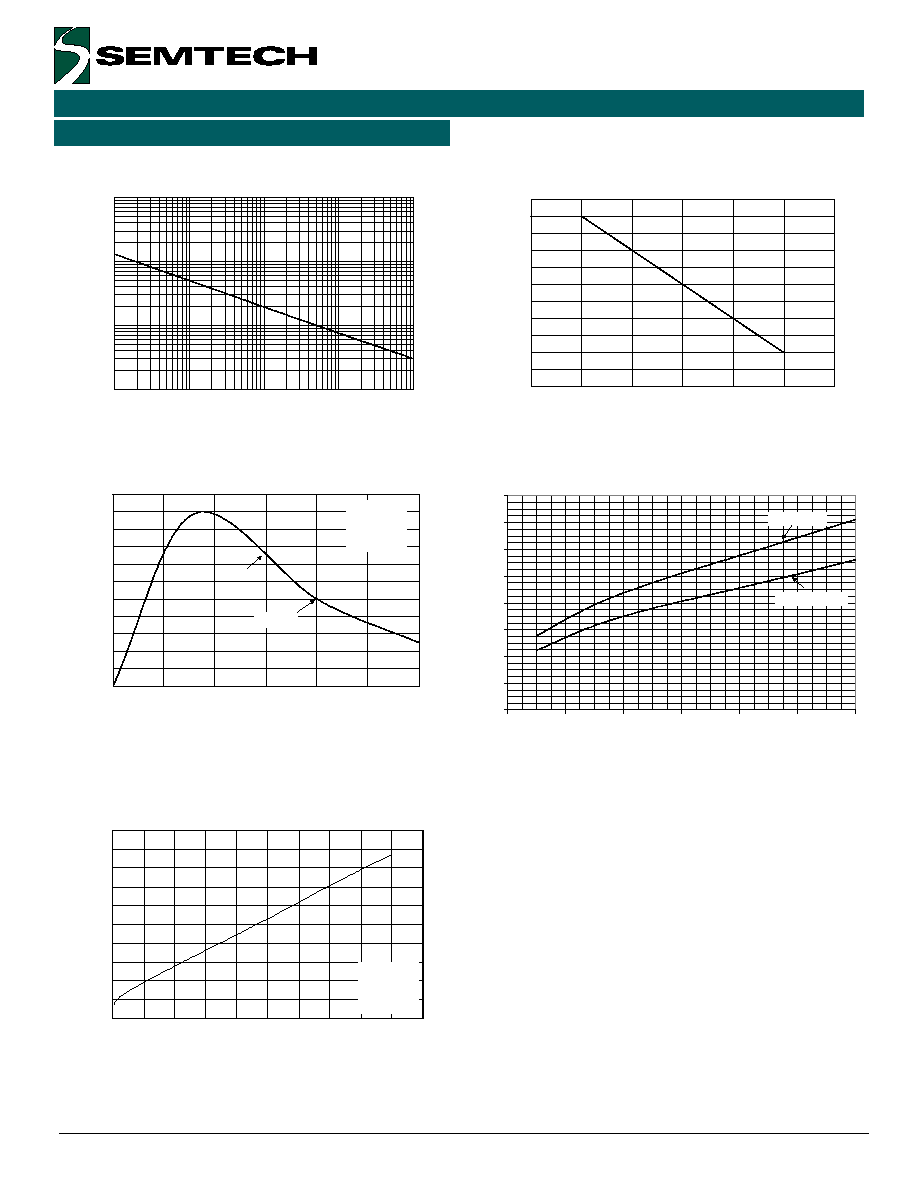
Typical Characteristics
Non-Repetitive Peak Pulse Power vs. Pulse Time
Power Derating Curve
0
10
20
30
40
50
60
70
80
90
100
110
0
25
50
75
100
125
150
Ambient Temperature - T
A
(
o
C)
% of Rated Power or I
PP
Clamping Voltage vs. Peak Pulse Current
0
10
20
30
40
50
60
70
80
90
100
110
0
5
10
15
20
25
30
Time (
�
�
�
�
s)
Percent of I
PP
e
-t
td = I
PP
/2
Waveform
Parameters:
tr = 8
�
s
td = 20
�
s
Pulse Waveform
0
2
4
6
8
10
12
14
16
0
2
4
6
8
10
12
Peak Pulse Current (A)
Clamping Voltage (V)
Line-To-Ground
Line-To-Line
Forward Voltage vs. Forward Current
0
1
2
3
4
5
6
7
8
9
10
0
5
10
15
20
25
30
35
40
45
50
Forward Current - I
F
(A)
Forward Voltage - V
F
(V)
Waveform
Parameters:
tr = 8
�
s
td = 20
�
s
0.01
0.1
1
10
0.1
1
10
100
1000
Pulse Duration - tp (
�
�
�
�
s)
Peak Pulse Power - P
PP
(kW)
4
2000 Semtech Corp.
www.semtech.com
PROTECTION PRODUCTS
SR3.3
PRELIMINARY
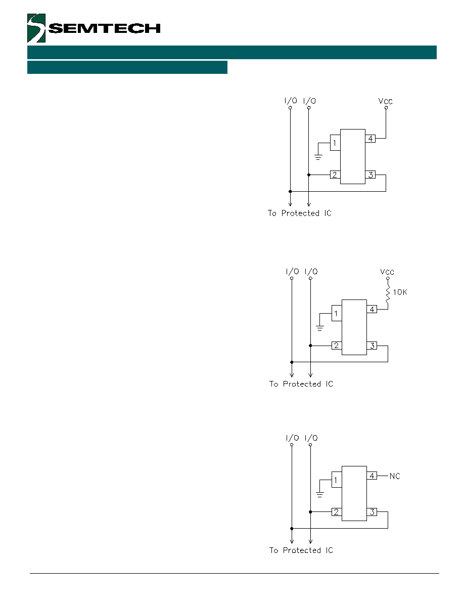
Data Line and Power Supply Protection Using
Data Line and Power Supply Protection Using
Data Line and Power Supply Protection Using
Data Line and Power Supply Protection Using
Data Line and Power Supply Protection Using
Vcc as reference
Vcc as reference
Vcc as reference
Vcc as reference
Vcc as reference
Data Line Protection with Bias and Power Sup-
Data Line Protection with Bias and Power Sup-
Data Line Protection with Bias and Power Sup-
Data Line Protection with Bias and Power Sup-
Data Line Protection with Bias and Power Sup-
ply Isolation Resistor
ply Isolation Resistor
ply Isolation Resistor
ply Isolation Resistor
ply Isolation Resistor
Data Line Pr
Data Line Pr
Data Line Pr
Data Line Pr
Data Line Proooootttttection Using Int
ection Using Int
ection Using Int
ection Using Int
ection Using Internal T
ernal T
ernal T
ernal T
ernal T VVVVVS Diode
S Diode
S Diode
S Diode
S Diode
as Reference
as Reference
as Reference
as Reference
as Reference
Device Connection Options for Protection of
Device Connection Options for Protection of
Device Connection Options for Protection of
Device Connection Options for Protection of
Device Connection Options for Protection of
T
T
T
T
Tw
w
w
w
wo High-Speed Data Lines
o High-Speed Data Lines
o High-Speed Data Lines
o High-Speed Data Lines
o High-Speed Data Lines
The SR3.3 TVS is designed to protect two data lines
from transient over-voltages by clamping them to a
fixed reference. When the voltage on the protected
line exceeds the reference voltage (plus diode V
F
) the
steering diodes are forward biased, conducting the
transient current away from the sensitive circuitry.
Data lines are connected at pins 2 and 3. The nega-
tive reference (REF1) is connected at pin 1. This pin
should be connected directly to a ground plane on the
board for best results. The path length is kept as short
as possible to minimize parasitic inductance.
The positive reference (REF2) is connected at pin 4.
The options for connecting the positive reference are
as follows:
1. To protect data lines and the power line, connect
pin 4 directly to the positive supply rail (V
CC
). In this
configuration the data lines are referenced to the
supply voltage. The internal TVS diode prevents
over-voltage on the supply rail.
2. The SR3.3 can be isolated from the power supply
by adding a series resistor between pin 4 and V
CC
.
A value of 10k
is recommended. The internal
TVS and steering diodes remain biased, providing
the advantage of lower capacitance.
3. In applications where no positive supply reference
is available, or complete supply isolation is desired,
the internal TVS may be used as the reference. In
this case, pin 4 is not connected. The steering
diodes will begin to conduct when the voltage on
the protected line exceeds the working voltage of
the TVS (plus one diode drop).
Board Layout Considerations for ESD Protection
Board Layout Considerations for ESD Protection
Board Layout Considerations for ESD Protection
Board Layout Considerations for ESD Protection
Board Layout Considerations for ESD Protection
Board layout plays an important role in the suppression
of extremely fast rise-time ESD transients. Recall that
the voltage developed across an inductive load is
proportional to the time rate of change of current
through the load (V = L di/dt). The total clamping
voltage seen by the protected load will be the sum of
Applications Information
5
2000 Semtech Corp.
www.semtech.com
PROTECTION PRODUCTS
SR3.3
PRELIMINARY
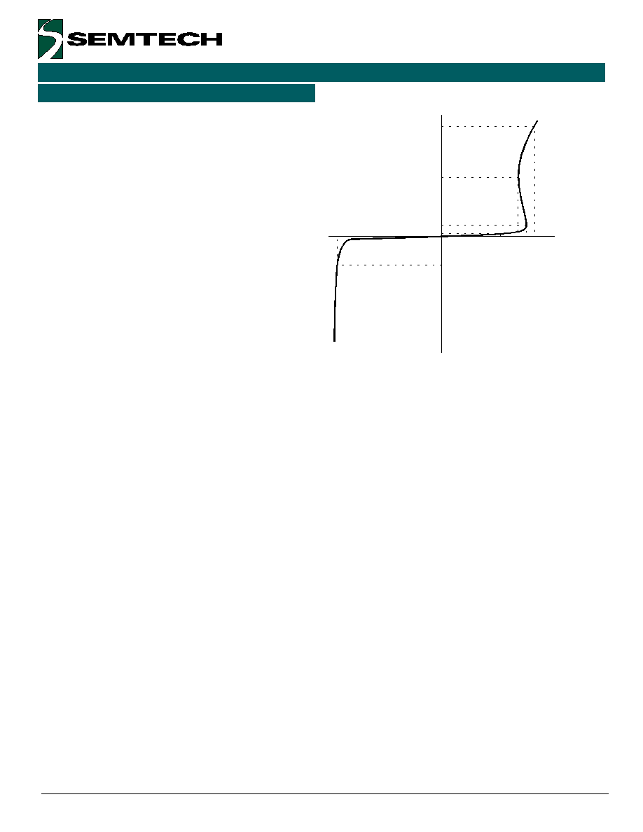
PIN Descriptions
Applications Information (continued)
I
P P
I
SB
I
PT
I
R
V
RWM
V
V
PT
V
C
V
BRR
I
BRR
SB
Figure 1 - EPD TVS IV Characteristic Curve
the TVS clamping voltage and the voltage due to the
parasitic inductance (V
C(TOT)
= V
C
+ L di/dt) . Parasitic
inductance in the protection path can result in signifi-
cant voltage overshoot, reducing the effectiveness of
the suppression circuit. An ESD induced transient for
example reaches a peak in approximately 1ns. For a
30A pulse (per IEC 61000-4-2 Level 4), 1nH of series
inductance will increase the effective clamping voltage
by 30V
(V = 1x10
-9
(30/1x10
-9
)). For maximum effectiveness,
the following board layout guidelines are recom-
mended:
"
Minimize the path length between the SR3.3 and
the protected line.
"
Place the SR3.3 near the RJ45 connector to
restrict transient coupling in nearby traces.
"
Minimize the path length (inductance) between the
RJ45 connector and the SR3.3.
EPD TVS Characteristics
The internal TVS of the SR3.3 is constructed using
Semtech's proprietary EPD technology. The structure
of the EPD TVS is vastly different from the traditional
pn-junction devices. At voltages below 5V, high leak-
age current and junction capacitance render conven-
tional avalanche technology impractical for most
applications. However, by utilizing the EPD technology,
the SR3.3 can effectively operate at 3.3V while main-
taining excellent electrical characteristics.
The EPD TVS employs a complex nppn structure in
contrast to the pn structure normally found in tradi-
tional silicon-avalanche TVS diodes. The EPD mecha-
nism is achieved by engineering the center region of
the device such that the reverse biased junction does
not avalanche, but will "punch-through" to a conduct-
ing state. This structure results in a device with supe-
rior dc electrical parameters at low voltages while
maintaining the capability to absorb high transient
currents.
The IV characteristic curve of the EPD device is shown
in Figure 1. The device represents a high impedance
to the circuit up to the working voltage (V
RWM
). During a
transient event, the device will begin to conduct as it is
biased in the reverse direction. When the punch-
through voltage (V
PT
) is exceeded, the device enters a
low impedance state, diverting the transient current
away from the protected circuit. When the device is
conducting current, it will exhibit a slight "snap-back" or
negative resistance characteristic due to its structure.
This must be considered when connecting the device
to a power supply rail. To return to a non-conducting
state, the current through the device must fall below
the snap-back current (approximately < 50mA).
6
2000 Semtech Corp.
www.semtech.com
PROTECTION PRODUCTS
SR3.3
PRELIMINARY
Notes:
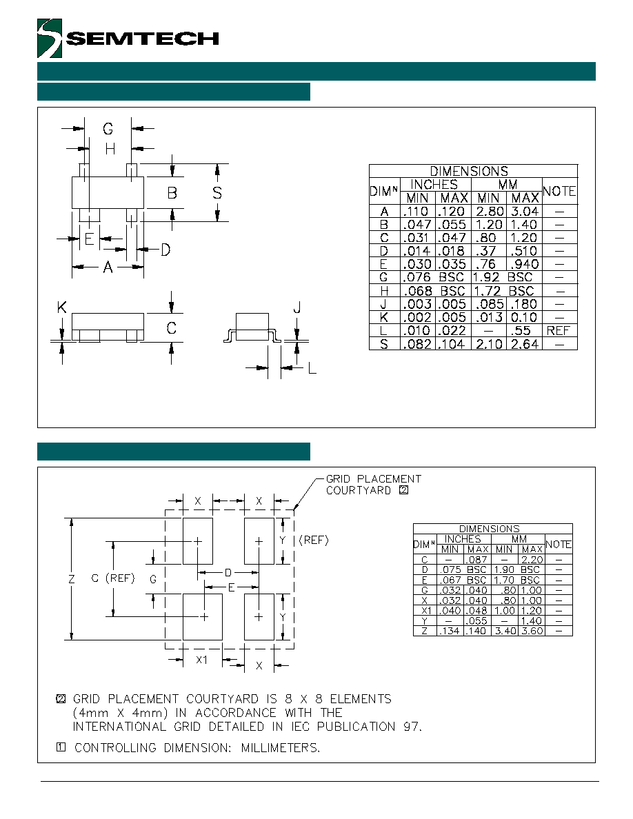
(1) Controlling dimension: Inch (unless otherwise specified).
(2) Dimension A and B do not include mold protrusions. Mold protrusions are .006" max.
Outline Drawing - SOT-143
Land Pattern - SOT-143

7
2000 Semtech Corp.
www.semtech.com
PROTECTION PRODUCTS
SR3.3
PRELIMINARY
Contact Information
Semtech Corporation
Protection Products Division
652 Mitchell Rd., Newbury Park, CA 91320
Phone: (805)498-2111 FAX (805)498-3804
t
r
a
P
r
e
b
m
u
N
g
n
i
k
r
o
W
e
g
a
t
l
o
V
r
e
p
y
t
Q
l
e
e
R
e
z
i
S
l
e
e
R
C
T
.
3
.
3
R
S
V
3
.
3
0
0
0
,
3
h
c
n
I
7
G
T
.
3
.
3
R
S
V
3
.
3
0
0
0
,
0
1
h
c
n
I
3
1
Marking Codes
r
e
b
m
u
N
t
r
a
P
g
n
i
k
r
a
M
e
d
o
C
3
.
3
R
S
3
.
3
R
Ordering Information