PROTECTION PRODUCTS
1
www.semtech.com
PROTECTION PRODUCTS
SRDA3.3-6 & SRDA05-6
RailClamp
“
Low Capacitance TVS Diode Array
Description
Features
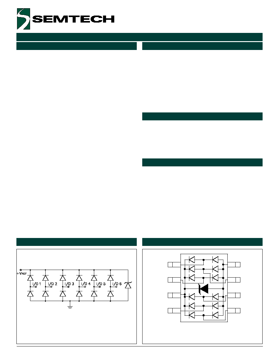
Circuit Diagram
Schematic & PIN Configuration
Revision 9/2000
RailClamps are surge rated diode arrays designed to
protect high speed data interfaces. The SR series has
been specifically designed to protect sensitive compo-
nents which are connected to data and transmission
lines from overvoltage caused by ESD (electrostatic
discharge), EFT (electrical fast transients), and light-
ning.
The unique design of the SRDA series devices incorpo-
rates surge rated, low capacitance steering diodes and
a TVS diode in a single package. During transient
conditions, the steering diodes direct the transient to
either the positive side of the power supply line or to
ground. The internal TVS diode prevents over-voltage
on the power line, protecting any downstream compo-
nents.
The low capacitance array configuration allows the user
to protect two high-speed data or transmission lines.
The low inductance construction minimizes voltage
overshoot during high current surges.
Applications
Mechanical Characteristics
u
USB Power & Data Line Protection
u
T1/E1 secondary IC Side Protection
u
Token Ring
u
HDSL, IDSL secondary IC Side Protection
u
Video Line Protection
u
Microcontroller Input Protection
u
Base stations
u
I
2
C Bus Protection
u
Transient protection for high-speed data lines to
IEC 61000-4-2 (ESD) 15kV (air), 8kV (contact)
IEC 61000-4-4 (EFT) 40A (5/50ns)
IEC 61000-4-5 (Lightning) 24A (8/20µs)
u
Array of surge rated diodes with internal TVS diode
u
Protects six I/O lines & power supply line
u
Low capacitance (<15pF) for high-speed interfaces
u
Low operating & clamping voltages
u
Solid-state technology
u
JEDEC SO-8 package
u
UL 497B listed
u
Molding compound flammability rating: UL 94V-0
u
Marking : Part number, date code, logo
u
Packaging : Tube or Tape and Reel per EIA 481
S0-8 (Top View)
I/O 1
I/O 2
I/O 3
I/O 4
I/O 5
I/O 6
+V
REF
GND
1
2
3
4
5
6
7
8

2
„ 2000 Semtech Corp.
www.semtech.com
PROTECTION PRODUCTS
PROTECTION PRODUCTS
SRDA3.3-6 & SRDA05-6
Absolute Maximum Rating
Electrical Characteristics
g
n
it
a
R
l
o
b
m
y
S
e
u
l
a
V
s
ti
n
U
)
s
µ
0
2
/
8
=
p
t(
r
e
w
o
P
e
s
l
u
P
k
a
e
P
P
k
p
0
0
5
s
tt
a
W
)
s
µ
0
2
/
8
=
p
t(
t
n
e
rr
u
C
e
s
l
u
P
k
a
e
P
I
P
P
5
2
A
I(
e
g
a
tl
o
V
d
r
a
w
r
o
F
k
a
e
P
F
)
s
µ
0
2
/
8
=
p
t
,
A
1
=
V
P
F
5
.
1
V
e
r
u
t
a
r
e
p
m
e
T
g
n
ir
e
d
l
o
S
d
a
e
L
T
L
).
c
e
s
0
1
(
0
6
2
C
∞
e
r
u
t
a
r
e
p
m
e
T
g
n
it
a
r
e
p
O
T
J
5
2
1
+
o
t
5
5
-
C
∞
e
r
u
t
a
r
e
p
m
e
T
e
g
a
r
o
t
S
T
G
T
S
0
5
1
+
o
t
5
5
-
C
∞
6
-
3
.
3
A
D
R
S
r
e
t
e
m
a
r
a
P
l
o
b
m
y
S
s
n
o
it
i
d
n
o
C
m
u
m
i
n
i
M
l
a
c
i
p
y
T
m
u
m
i
x
a
M
s
ti
n
U
e
g
a
tl
o
V
ff
O
-
d
n
a
t
S
e
s
r
e
v
e
R
V
M
W
R
3
.
3
V
e
g
a
tl
o
V
h
g
u
o
r
h
T
-
h
c
n
u
P
V
T
P
I
T
P
A
µ
2
=
5
.
3
V
e
g
a
tl
o
V
k
c
a
B
-
p
a
n
S
V
B
S
I
B
S
A
m
0
5
=
8
.
2
V
t
n
e
rr
u
C
e
g
a
k
a
e
L
e
s
r
e
v
e
R
I
R
V
M
W
R
C
∞
5
2
=
T
,
V
3
.
3
=
1
A
µ
e
g
a
tl
o
V
g
n
i
p
m
a
l
C
V
C
I
P
P
s
µ
0
2
/
8
=
p
t
,
A
1
=
3
.
5
V
e
g
a
tl
o
V
g
n
i
p
m
a
l
C
V
C
I
P
P
s
µ
0
2
/
8
=
p
t
,
A
0
1
=
0
1
V
e
g
a
tl
o
V
g
n
i
p
m
a
l
C
V
C
I
P
P
s
µ
0
2
/
8
=
p
t
,
A
5
2
=
5
1
V
e
c
n
a
ti
c
a
p
a
C
n
o
it
c
n
u
J
C
j
d
n
a
s
n
i
p
O
/
I
n
e
e
w
t
e
B
d
n
G
V
R
z
H
M
1
=
f
,
V
0
=
8
5
1
F
p
s
n
i
p
O
/
I
n
e
e
w
t
e
B
V
R
z
H
M
1
=
f
,
V
0
=
4
F
p
Note:
(1) The SRDA3.3-6 is constructed using Semtechs propri-
etary EPD process technology. See applications section for
more information.

3
„ 2000 Semtech Corp.
www.semtech.com
PROTECTION PRODUCTS
PROTECTION PRODUCTS
SRDA3.3-6 & SRDA05-6
6
-
5
0
A
D
R
S
r
e
t
e
m
a
r
a
P
l
o
b
m
y
S
s
n
o
it
i
d
n
o
C
m
u
m
i
n
i
M
l
a
c
i
p
y
T
m
u
m
i
x
a
M
s
ti
n
U
e
g
a
tl
o
V
ff
O
-
d
n
a
t
S
e
s
r
e
v
e
R
V
M
W
R
5
V
e
g
a
tl
o
V
n
w
o
d
k
a
e
r
B
e
s
r
e
v
e
R
V
R
B
I
t
A
m
1
=
6
V
t
n
e
rr
u
C
e
g
a
k
a
e
L
e
s
r
e
v
e
R
I
R
V
M
W
R
C
∞
5
2
=
T
,
V
5
=
0
1
A
µ
e
g
a
tl
o
V
g
n
i
p
m
a
l
C
V
C
I
P
P
s
µ
0
2
/
8
=
p
t
,
A
1
=
8
.
9
V
e
g
a
tl
o
V
g
n
i
p
m
a
l
C
V
C
I
P
P
s
µ
0
2
/
8
=
p
t
,
A
0
1
=
2
1
V
e
g
a
tl
o
V
g
n
i
p
m
a
l
C
V
C
I
P
P
s
µ
0
2
/
8
=
p
t
,
A
5
2
=
0
2
V
e
c
n
a
ti
c
a
p
a
C
n
o
it
c
n
u
J
C
j
d
n
a
s
n
i
p
O
/
I
n
e
e
w
t
e
B
d
n
G
V
R
z
H
M
1
=
f
,
V
0
=
8
5
1
F
p
s
n
i
p
O
/
I
n
e
e
w
t
e
B
V
R
z
H
M
1
=
f
,
V
0
=
4
F
p
Electrical Characteristics (continued)
4
„ 2000 Semtech Corp.
www.semtech.com
PROTECTION PRODUCTS
PROTECTION PRODUCTS
SRDA3.3-6 & SRDA05-6
Typical Characteristics
Non-Repetitive Peak Pulse Power vs. Pulse Time
Power Derating Curve
0.01
0.1
1
10
0.1
1
10
100
1000
Pulse Duration - tp (
µ
s)
Peak Pulse Power - P
PP
(kW)
0
10
20
30
40
50
60
70
80
90
100
110
0
25
50
75
100
125
150
Ambient Temperature - T
A
(
o
C)
% of Rated Power or I
PP
Clamping Voltage vs. Peak Pulse Current
0
10
20
30
40
50
60
70
80
90
100
110
0
5
10
15
20
25
30
Time (
µ
s)
Percent of I
PP
e
-t
td = I
PP
/2
Waveform
Parameters:
tr = 8
µ
s
td = 20
µ
s
Pulse Waveform
Variation of Capacitance vs. Reverse Voltage
Forward Voltage vs. Forward Current
-14
-12
-10
-8
-6
-4
-2
0
0
1
2
3
4
5
6
Reverse Voltage (V)
% Change in Capacitance
I/O to GND
f = 1MHz
0
1
2
3
4
5
6
7
8
9
10
0
5
10
15
20
25
30
35
40
45
50
Forward Current - I
F
(A)
Forward Voltage - V
F
(V)
Waveform
Parameters:
tr = 8
µ
s
td = 20
µ
s
0
2
4
6
8
10
12
14
16
18
0
5
10
15
20
25
30
35
Peak Pulse Current - I
PP
(A)
Clamping Voltage - V
C
(V)
SRDA05-6
SRDA3.3-6
Waveform
Parameters:
tr = 8
µ
s
td = 20
µ
s
5
„ 2000 Semtech Corp.
www.semtech.com
PROTECTION PRODUCTS
PROTECTION PRODUCTS
SRDA3.3-6 & SRDA05-6
Device Connection Options for Protection of Six High-
Speed Lines
The SRDA TVS is designed to protect four data lines
from transient overvoltages by clamping them to a
fixed reference. When the voltage on the protected
line exceeds the reference voltage (plus diode V
F
) the
steering diodes are forward biased, conducting the
transient current away from the sensitive circuitry.
Data lines are connected at pins 1, 2, 4, 5, 6 and 7.
The negative reference is connected at pin 8. These
pins should be connected directly to a ground plane on
the board for best results. The path length is kept as
short as possible to minimize parasitic inductance.
The positive reference is connected at pins 2 and 3.
The options for connecting the positive reference are
as follows:
1. To protect data lines and the power line, connect
pin 3 directly to the positive supply rail (V
CC
). In this
configuration the data lines are referenced to the
supply voltage. The internal TVS diode prevents
over-voltage on the supply rail.
2. The SRDA can be isolated from the power supply by
adding a series resistor between pin 3 and V
CC
. A
value of 10kW is recommended. The internal TVS
and steering diodes remain biased, providing the
advantage of lower capacitance.
3. In applications where no positive supply reference
is available, or complete supply isolation is desired,
the internal TVS may be used as the reference. In
this case, pin 3 is not connected. The steering
diodes will begin to conduct when the voltage on
the protected line exceeds the working voltage of
the TVS (plus one diode drop).
ESD Protection With RailClamps
Data Line and Power Supply Protection Using Vcc as
reference
Data Line Protection with Bias and Power Supply
Isolation Resistor
Data Line Protection Using Internal TVS Diode as
Reference
RailClamps are optimized for ESD protection using the
rail-to-rail topology. Along with good board layout,
these devices virtually eliminate the disadvantages of
using discrete components to implement this topology.
Consider the situation shown in Figure 1 where dis-
crete diodes or diode arrays are configured for rail-to-
rail protection on a high speed line. During positive
duration ESD events, the top diode will be forward
biased when the voltage on the protected line exceeds
the reference voltage plus the V
F
drop of the diode.
For negative events, the bottom diode will be biased
when the voltage exceeds the V
F
of the diode. At first
Applications Information
6
„ 2000 Semtech Corp.
www.semtech.com
PROTECTION PRODUCTS
PROTECTION PRODUCTS
SRDA3.3-6 & SRDA05-6
PIN Descriptions
Figure 1 - Rail-To-Rail Protection Topology
(First Approximation)
Figure 2 - The Effects of Parasitic Inductance When
Using Discrete Components to Implement Rail-To-Rail
Protection
Figure 3 - Rail-To-Rail Protection Using
RailClamp TVS Arrays
Applications Information (continued)
approximation, the clamping voltage due to the charac-
teristics of the protection diodes is given by:
V
C
= V
CC
+ V
F
(for positive duration pulses)
V
C
= -V
F
(for negative duration pulses)
However, for fast rise time transient events, the
effects of parasitic inductance must also be consid-
ered as shown in Figure 2. Therefore, the actual
clamping voltage seen by the protected circuit will be:
V
C
= V
CC
+ V
F
+ L
P
di
ESD
/dt (for positive duration pulses)
V
C
= -V
F
- L
G
di
ESD
/dt
(for negative duration pulses)
ESD current reaches a peak amplitude of 30A in 1ns
for a level 4 ESD contact discharge per IEC 1000-4-2.
Therefore, the voltage overshoot due to 1nH of series
inductance is:
V = L
P
di
ESD
/dt = 1X10
-9
(30 / 1X10
-9
) = 30V
Example:
Consider a V
CC
= 5V, a typical V
F
of 30V (at 30A) for the
steering diode and a series trace inductance of 10nH.
The clamping voltage seen by the protected IC for a
positive 8kV (30A) ESD pulse will be:
V
C
= 5V + 30V + (10nH X 30V/nH) = 335V
This does not take into account that the ESD current is
directed into the supply rail, potentially damaging any
components that are attached to that rail. Also note
the high V
F
of the discrete diode. It is not uncommon
for the V
F
of discrete diodes to exceed the damage
threshold of the protected IC. This is due to the
relatively small junction area of typical discrete compo-
nents. It is also possible that the power dissipation
capability of the discrete diode will be exceeded, thus
destroying the device.
The RailClamp is designed to overcome the inherent
disadvantages of using discrete signal diodes for ESD
suppression. The RailClamps integrated TVS diode
helps to mitigate the effects of parasitic inductance in
the power supply connection. During an ESD event,

7
„ 2000 Semtech Corp.
www.semtech.com
PROTECTION PRODUCTS
PROTECTION PRODUCTS
SRDA3.3-6 & SRDA05-6
Applications Information (continued)
the current will be directed through the integrated TVS
diode to ground. The total clamping voltage seen by
the protected IC due to this path will be:
V
C
= V
F(RailClamp)
+ V
TVS
This is given in the data sheet as the rated clamping
voltage of the device. For an SRDA05-6 the typical
clamping voltage is <16V at I
PP
=30A. The diodes
internal to the RailClamp are low capacitance, fast
switching devices that are rated to handle high tran-
sient currents and maintain excellent forward voltage
characteristics.
Using the RailClamp does not negate the need for good
board layout. All other inductive paths must be consid-
ered. The connection between the positive supply and
the SRDA and from the ground plane to the SRDA
must be kept as short as possible. The path between
the SRDA and the protected line must also be mini-
mized. The protected lines should be routed directly to
the SRDA. Placement of the SRDA on the PC board is
also critical for effective ESD protection. The device
should be placed as close as possible to the input
connector. The reason for this is twofold. First,
inductance resists change in current flow. If a signifi-
cant inductance exists between the connector and the
TVS, the ESD current will be directed elsewhere (lower
resistance path) in the system. Second, the effects of
radiated emissions and transient coupling can cause
upset to other areas of the board even if there is no
direct path to the connector. By placing the TVS close
to the connector it will divert the ESD current immedi-
ately and absorb the ESD energy before it can be
coupled into nearby traces.
(Reference Semtech application note SI99-01 for
further information on board layout)
the EPD technology, the SRDA3.3-6 can effectively
operate at 3.3V while maintaining excellent electrical
characteristics.
The IV characteristic curve of the EPD device is shown
in Figure 4. The device represents a high impedance
to the circuit up to the working voltage (V
RWM
). During a
transient event, the device will begin to conduct as it is
biased in the reverse direction. When the punch-
through voltage (V
PT
) is exceeded, the device enters a
low impedance state, diverting the transient current
away from the protected circuit. When the device is
conducting current, it will exhibit a slight snap-back or
negative resistance characteristic due to its structure.
This must be considered when connecting the device
to a power supply rail. To return to a non-conducting
state, the current through the device must fall below
the snap-back current (approximately < 50mA) to allow
it to travel back through the negative resistance
region. If this is a concern, a 10kW current limiting
resistor can be placed between the supply rail and the
positive reference pin to prevent device latch-up.
RailClamp is a registered trademark of Semtech corporation
,
PP
,
6%
,
37
,
5
9
5:0
9
9
37
9
&
9
%55
,
%55
6%
Figure 4 - EPD TVS IV Characteristic Curve
SRDA3.3-6 EPD TVS Characteristics
The internal TVS of the SRDA3.3-4 is constructed using
Semtechs proprietary EPD technology. The structure
of the EPD TVS is vastly different from the traditional
pn-junction devices that are internal to the SRDA05-6.
At voltages below 5V, high leakage current and junction
capacitance render conventional avalanche technology
impractical for most applications. However, by utilizing
8
„ 2000 Semtech Corp.
www.semtech.com
PROTECTION PRODUCTS
PROTECTION PRODUCTS
SRDA3.3-6 & SRDA05-6
Video Line Protection
Typical Applications
9
„ 2000 Semtech Corp.
www.semtech.com
PROTECTION PRODUCTS
PROTECTION PRODUCTS
SRDA3.3-6 & SRDA05-6
Notes:
(1) Controlling dimension: Inch (unless otherwise specified).
Outline Drawing - SO-8
Land Pattern - SO-8

10
„ 2000 Semtech Corp.
www.semtech.com
PROTECTION PRODUCTS
PROTECTION PRODUCTS
SRDA3.3-6 & SRDA05-6
Contact Information
Semtech Corporation
Protection Products Division
652 Mitchell Rd., Newbury Park, CA 91320
Phone: (805)498-2111 FAX (805)498-3804
Ordering Information
r
e
b
m
u
N
t
r
a
P
g
n
i
k
r
o
W
e
g
a
tl
o
V
r
e
p
y
t
Q
l
e
e
R
e
z
i
S
l
e
e
R
B
T
.
6
-
3
.
3
A
D
R
S
V
3
.
3
0
0
5
h
c
n
I
7
E
T
.
6
-
3
.
3
A
D
R
S
V
3
.
3
0
0
5
2
h
c
n
I
3
1
B
T
.
6
-
5
0
A
D
R
S
V
5
0
0
5
h
c
n
I
7
E
T
.
6
-
5
0
A
D
R
S
V
5
0
0
5
2
h
c
n
I
3
1
Note:
(1) No suffix indicates tube pack.