1
www.semtech.com
PROTECTION PRODUCTS
SRV05-4
RailClamp
Low Capacitance TVS Diode Array
Description
Features
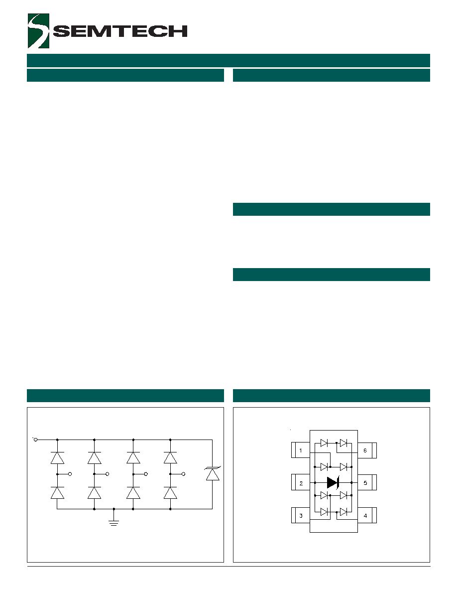
Circuit Diagram
Schematic and PIN Configuration
Revision 08/11/04
RailClamps are surge rated diode arrays designed to
protect high speed data interfaces. The SR series has
been specifically designed to protect sensitive compo-
nents which are connected to data and transmission
lines from overvoltage caused by electrostatic dis-
charge (ESD), electrical fast transients (EFT), and
lightning.
The unique design of the SR series devices incorpo-
rates eight surge rated, low capacitance steering
diodes and a TVS diode in a single package. During
transient conditions, the steering diodes direct the
transient to either the positive side of the power supply
line or to ground. The internal TVS diode prevents
over-voltage on the power line, protecting any down-
stream components.
The SRV05-4 has a low typical capacitance of 3pF and
operates with virtually no insertion loss to 1GHz. This
makes the device ideal for protection of high-speed
data lines such as USB 2.0, Firewire, DVI, and gigabit
Ethernet interfaces.
The low capacitance array configuration allows the user
to protect four high-speed data or transmission lines.
The low inductance construction minimizes voltage
overshoot during high current surges. They may be
used to meet the ESD immunity requirements of IEC
61000-4-2, Level 4 (±15kV air, ±8kV contact dis-
charge).
Applications
Mechanical Characteristics
USB 2.0 Power and Data Line Protection
Video Graphics Cards
Monitors and Flat Panel Displays
Digital Video Interface (DVI)
10/100/1000 Ethernet
Notebook Computers
SIM Ports
ATM Interfaces
IEEE 1394 Firewire Ports
ESD protection for high-speed data lines to
IEC 61000-4-2 (ESD) ±15kV (air), ±8kV (contact)
IEC 61000-4-4 (EFT) 40A (5/50ns)
IEC 61000-4-5 (Lightning) 12A (8/20µs)
Array of surge rated diodes with internal TVS Diode
Small package saves board space
Protects four I/O lines
Low capacitance: 3pF typical
Low clamping voltage
Low operating voltage: 5.0V
Solid-state silicon-avalanche technology
JEDEC SOT-23 6L package
Molding compound flammability rating: UL 94V-0
Marking : V05
Packaging : Tape and Reel per EIA 481
SOT-23 6L (Top View)
5
1
3
4
6
2
3
2004 Semtech Corp.
www.semtech.com
PROTECTION PRODUCTS
SRV05-4
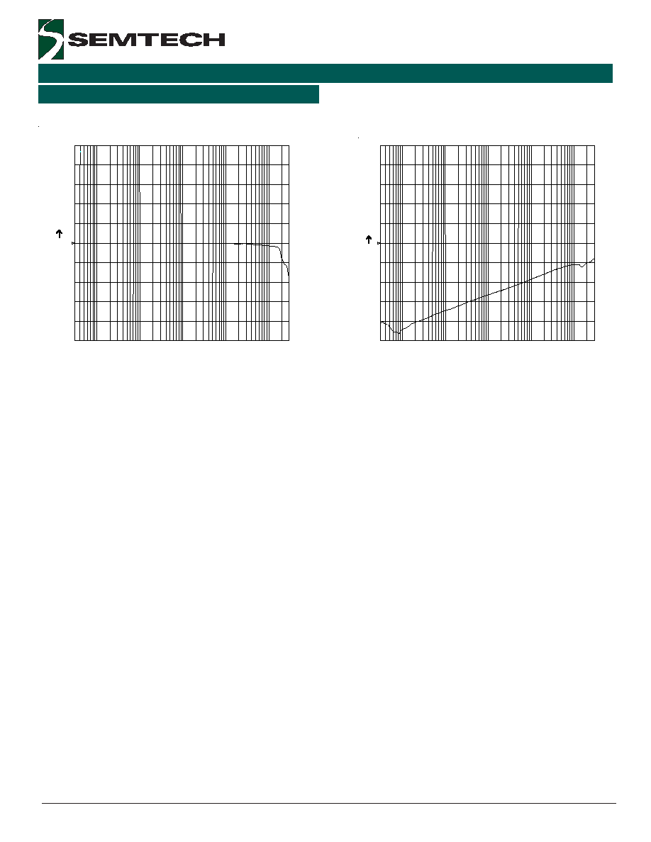
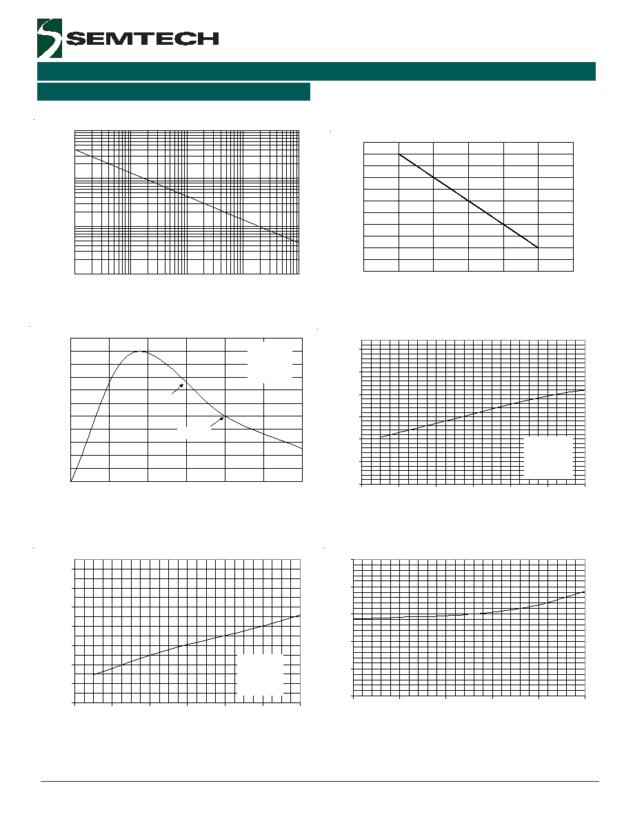
Typical Characteristics
Non-Repetitive Peak Pulse Power vs. Pulse Time
Power Derating Curve
0
10
20
30
40
50
60
70
80
90
100
110
0
25
50
75
100
125
150
Ambient Temperature - T
A
(
o
C)
%
of
Ra
t
e
d P
o
w
e
r or I
PP
Clamping Voltage vs. Peak Pulse Current
Pulse Waveform
Forward Voltage vs. Forward Current
Capacitance vs. Reverse Voltage
0
1
2
3
4
5
0
1
2
3
4
5
Reverse Voltage - V
R
(V)
C
a
p
aci
t
a
n
c
e -
C
j
(
pF)
0.00
5.00
10.00
15.00
20.00
25.00
30.00
0.00
2.00
4.00
6.00
8.00
10.00
12.00
Peak Pulse Current - I
PP
(A)
C
l
a
m
ping
V
o
l
t
a
g
e
-
V
C
(V)
Waveform
Parameters:
tr = 8µs
td = 20µs
0.00
1.00
2.00
3.00
4.00
5.00
6.00
7.00
0.00
2.00
4.00
6.00
8.00
10.00
12.00
Forward Current - I
F
(A)
F
o
r
w
ar
d
V
o
l
t
ag
e -
V
F
(V)
Waveform
Parameters:
tr = 8µs
td = 20µs
0.01
0.1
1
10
0.1
1
10
100
1000
Pulse Duration - tp (µs)
Pe
a
k
P
u
l
s
e
Po
w
e
r
-
P
Pk
(k
W
)
0
10
20
30
40
50
60
70
80
90
100
110
0
5
10
15
20
25
30
Time (µs)
Per
c
en
t
of
I
PP
e
-t
td = I
PP
/2
Waveform
Parameters:
tr = 8µs
td = 20µs

5
2004 Semtech Corp.
www.semtech.com
PROTECTION PRODUCTS
SRV05-4
Device Connection Options for Protection of Four
High-Speed Data Lines
The SRV05-4 TVS is designed to protect four data lines
from transient over-voltages by clamping them to a
fixed reference. When the voltage on the protected
line exceeds the reference voltage (plus diode V
F
) the
steering diodes are forward biased, conducting the
transient current away from the sensitive circuitry.
Data lines are connected at pins 1, 3, 4 and 6. The
negative reference (REF1) is connected at pin 2. This
pin should be connected directly to a ground plane on
the board for best results. The path length is kept as
short as possible to minimize parasitic inductance.
The positive reference (REF2) is connected at pin 5.
The options for connecting the positive reference are
as follows:
1. To protect data lines and the power line, connect
pin 5 directly to the positive supply rail (V
CC
). In this
configuration the data lines are referenced to the
supply voltage. The internal TVS diode prevents
over-voltage on the supply rail.
2. The SRV05-4 can be isolated from the power
supply by adding a series resistor between pin 5
and V
CC
. A value of 100k
is recommended. The
internal TVS and steering diodes remain biased,
providing the advantage of lower capacitance.
3. In applications where no positive supply reference
is available, or complete supply isolation is desired,
the internal TVS may be used as the reference. In
this case, pin 5 is not connected. The steering
diodes will begin to conduct when the voltage on
the protected line exceeds the working voltage of
the TVS (plus one diode drop).
ESD Protection With RailClamps
RailClamps are optimized for ESD protection using the
rail-to-rail topology. Along with good board layout,
these devices virtually eliminate the disadvantages of
using discrete components to implement this topology.
Consider the situation shown in Figure 1 where dis-
crete diodes or diode arrays are configured for rail-to-
rail protection on a high speed line. During positive
duration ESD events, the top diode will be forward
biased when the voltage on the protected line exceeds
Data Line and Power Supply Protection Using Vcc as
reference
Data Line Protection with Bias and Power Supply
Isolation Resistor
Data Line Protection Using Internal TVS Diode as
Reference
Applications Information