1
www.semtech.com
PROTECTION PRODUCTS
SRV08-4
RailClamp
Low Capacitance TVS Diode Array
Description
Features
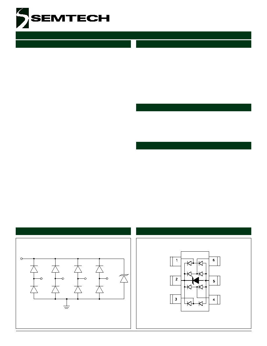
Circuit Diagram
Schematic & PIN Configuration
Revision 06/25/2002
RailClamps are surge rated diode arrays designed to
protect high speed data interfaces. The SR series has
been specifically designed to protect sensitive compo-
nents which are connected to data and transmission
lines from overvoltage caused by ESD (electrostatic
discharge), EFT (electrical fast transients), and light-
ning.
The unique design of the SRV08-4 integrates eight
surge rated, low capacitance steering diodes with a
TVS diode in a SOT23- 6L package. During transient
conditions, the steering diodes direct the transient to
either the positive side of the power supply line or to
ground. The internal TVS diode prevents over-voltage
on the power line, protecting any downstream compo-
nents.
The low capacitance array configuration allows the user
to protect four high-speed data or transmission lines.
The low inductance construction minimizes voltage
overshoot during high current surges.
Applications
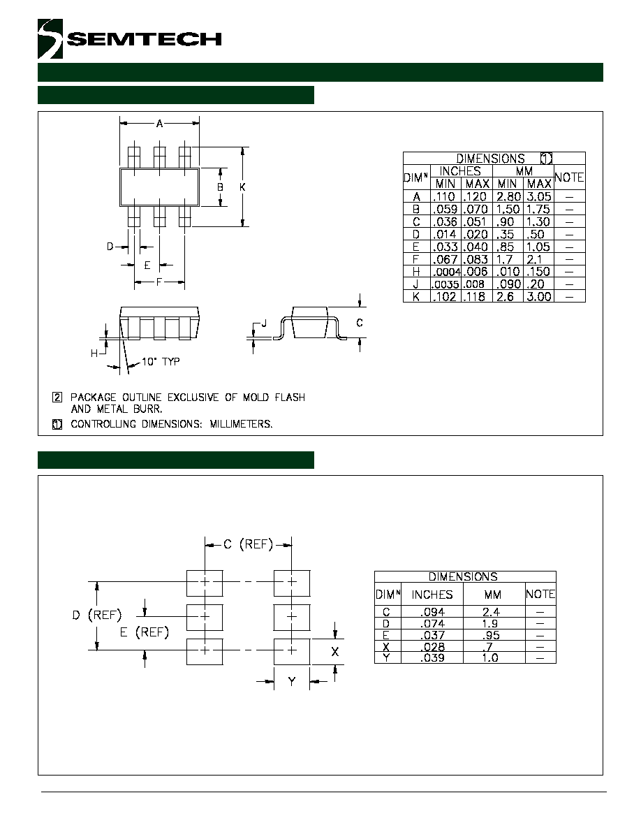
Mechanical Characteristics
USB Ports
Video Graphics Cards
Monitors and Flat Panel Displays
Digital Video Interface (DVI)
Cellular Handsets
Notebook Computers
Portable Electronics
Microcontroller Input Protection
ESD protection to IEC 61000-4-2, Level 4
Array of surge rated diodes with internal TVS Diode
Small package saves board space
Protects four I/O lines
Low capacitance (<5pF) for high-speed interfaces
Low clamping voltage
Low operating voltage: 5.0V
Solid-state silicon-avalanche technology
JEDEC SOT-23 6L package
Molding compound flammability rating: UL 94V-0
Marking : V08
Packaging : Tape and Reel per EIA 481
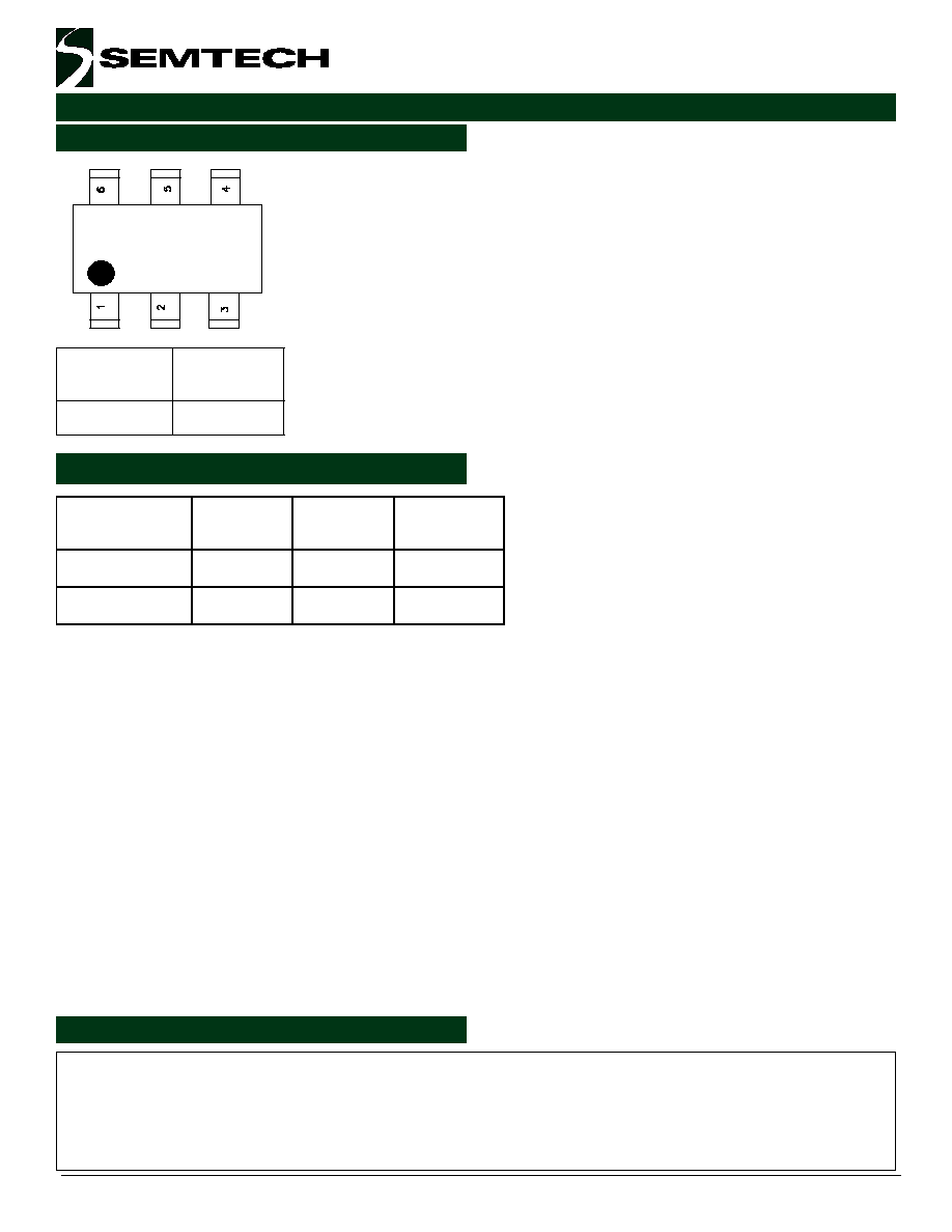
SOT-23 6L (Top View)
2
1
3
4
6
5
4
2002 Semtech Corp.
www.semtech.com
PROTECTION PRODUCTS
SRV08-4
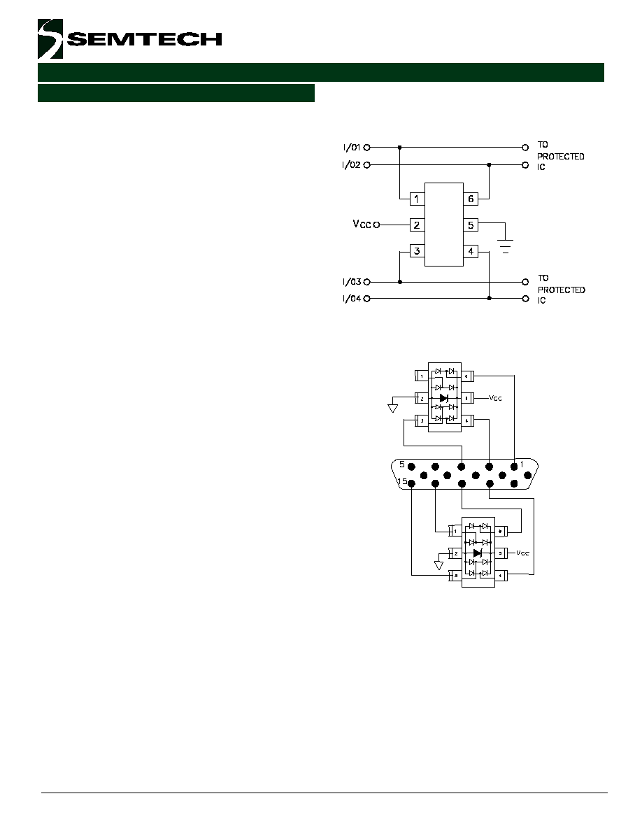
Device Connection Options for Protection of Four
High-Speed Data Lines
The SRV08-4 TVS is designed to protect four data lines
from transient over-voltages by clamping them to a
fixed reference. When the voltage on the protected
line exceeds the reference voltage (plus diode V
F
) the
steering diodes are forward biased, conducting the
transient current away from the sensitive circuitry.
Data lines are connected at pins 1, 3, 4 and 6. The
negative reference is connected at pin 5. This pin
should be connected directly to a ground plane on the
board for best results. The path length is kept as short
as possible to minimize parasitic inductance.
The positive reference is connected at pin 2. In this
configuration the data lines are referenced to the
supply voltage.
Video Interface Protection
Video interfaces are susceptible to transient voltages
resulting from electrostatic discharge (ESD) and "hot
plugging" cables. If left unprotected, the video
interface IC may be damaged or even destroyed.
Protecting a high-speed video port presents some
unique challenges. First, any added protection device
must have extremely low capacitance and low leakage
current so that the integrity of the video signal is not
compromised. Second, the protection component
must be able to absorb high voltage transients without
damage or degradation. As a minimum, the device
should be rated to handle ESD voltages per IEC
61000-4-2, level 4 (15kV air, 8kV contact). The
clamping voltage of the device (when conducting high
current ESD pulses) must be sufficiently low enough to
protect the sensitive CMOS IC. If the clamping voltage
is too high, the "protected" device may latch-up or be
destroyed. Finally, the device must take up a relatively
small amount of board space, particularly in portable
applications such as notebooks and handhelds. The
SRV08-4 is designed to meet or exceed all of the
above criteria. A typical video interface protection
circuit is shown in Figure 2. All exposed lines are
protected including R, G, B, H-Sync, V-Sync , and the ID
lines for plug and play monitors.
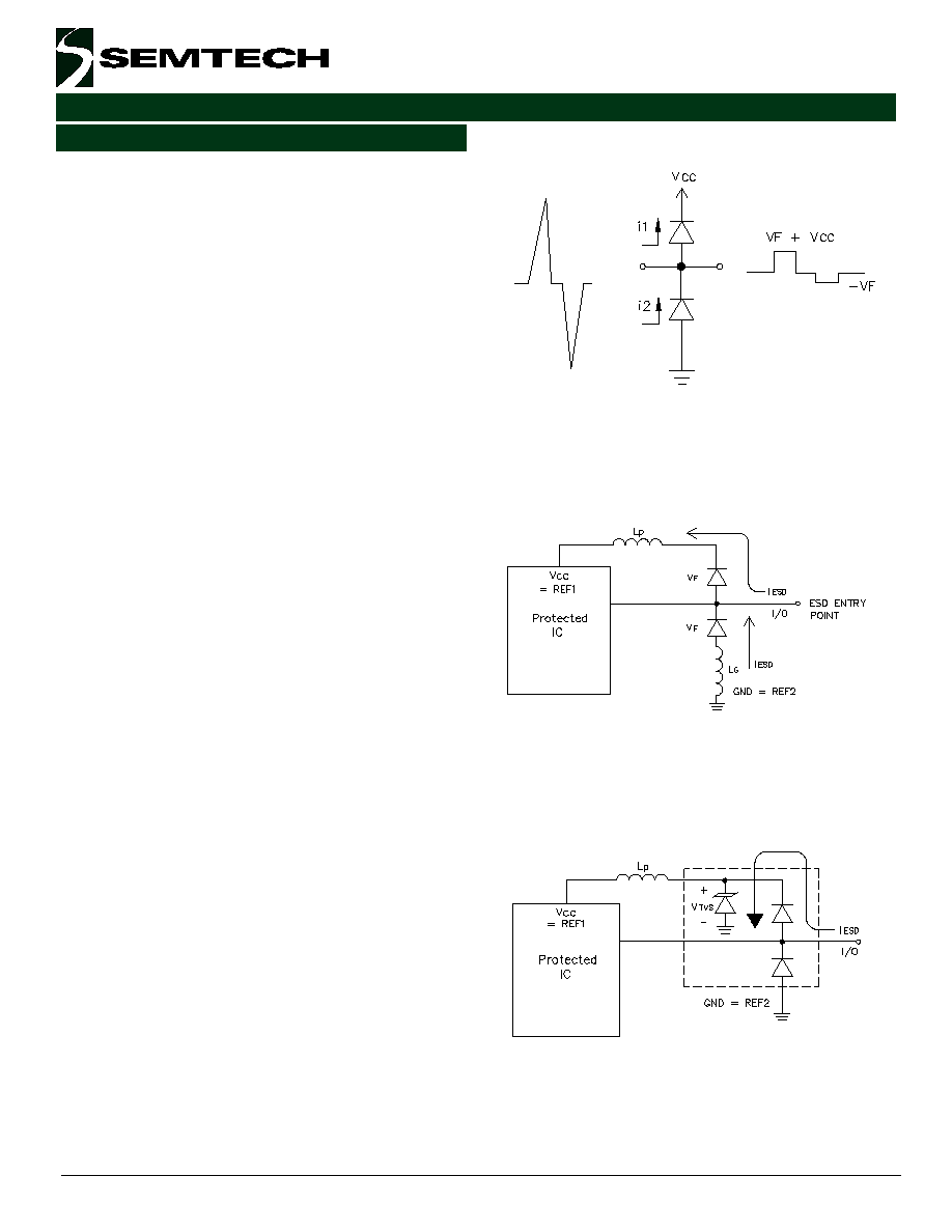
ESD Protection With RailClamps
RailClamps are optimized for ESD protection using the
rail-to-rail topology. Along with good board layout,
Figure 1 - Data Line and Power Supply Protection
Using Vcc as reference
Figure 2 - Video Interface Protection
Applications Information
5
2002 Semtech Corp.
www.semtech.com
PROTECTION PRODUCTS
SRV08-4
PIN Descriptions
these devices virtually eliminate the disadvantages of
using discrete components to implement this topology.
Consider the situation shown in Figure 3 where dis-
crete diodes or diode arrays are configured for rail-to-
rail protection on a high speed line. During positive
duration ESD events, the top diode will be forward
biased when the voltage on the protected line exceeds
the reference voltage plus the V
F
drop of the diode.
For negative events, the bottom diode will be biased
when the voltage exceeds the V
F
of the diode. At first
approximation, the clamping voltage due to the charac-
teristics of the protection diodes is given by:
V
C
= V
CC
+ V
F
(for positive duration pulses)
V
C
= -V
F
(for negative duration pulses)
However, for fast rise time transient events, the
effects of parasitic inductance must also be consid-
ered as shown in Figure 4. Therefore, the actual
clamping voltage seen by the protected circuit will be:
V
C
= V
CC
+ V
F
+ L
P
di
ESD
/dt (for positive duration pulses)
V
C
= -V
F
- L
G
di
ESD
/dt
(for negative duration pulses)
ESD current reaches a peak amplitude of 30A in 1ns
for a level 4 ESD contact discharge per IEC 61000-4-2.
Therefore, the voltage overshoot due to 1nH of series
inductance is:
V = L
P
di
ESD
/dt = 1X10
-9
(30 / 1X10
-9
) = 30V
Example:
Consider a V
CC
= 5V, a typical V
F
of 30V (at 30A) for the
steering diode and a series trace inductance of 10nH.
The clamping voltage seen by the protected IC for a
positive 8kV (30A) ESD pulse will be:
V
C
= 5V + 30V + (10nH X 30V/nH) = 335V
Note that it is not uncommon for the V
F
of discrete
diodes to exceed the damage threshold of the pro-
tected IC. This is due to the relatively small junction
area of typical discrete components. It is also possible
that the power dissipation capability of the discrete
diode will be exceeded, thus destroying the device.
The RailClamp is designed to overcome the inherent
disadvantages of using discrete signal diodes for ESD
suppression.
Figure 3 - "Rail-
Figure 3 - "Rail-
Figure 3 - "Rail-
Figure 3 - "Rail-
Figure 3 - "Rail-TTTTTo-Rail" Pr
o-Rail" Pr
o-Rail" Pr
o-Rail" Pr
o-Rail" Proooootttttection T
ection T
ection T
ection T
ection Topology
opology
opology
opology
opology
(First Approximation)
(First Approximation)
(First Approximation)
(First Approximation)
(First Approximation)
Figure 4 - The Effects of Parasitic Inductance
Figure 4 - The Effects of Parasitic Inductance
Figure 4 - The Effects of Parasitic Inductance
Figure 4 - The Effects of Parasitic Inductance
Figure 4 - The Effects of Parasitic Inductance
When Using Discrete Components to Implement
When Using Discrete Components to Implement
When Using Discrete Components to Implement
When Using Discrete Components to Implement
When Using Discrete Components to Implement
Rail-
Rail-
Rail-
Rail-
Rail-TTTTTo-Rail Pr
o-Rail Pr
o-Rail Pr
o-Rail Pr
o-Rail Proooootttttection
ection
ection
ection
ection
Applications Information (continued)
Figure 5 - Rail-
Figure 5 - Rail-
Figure 5 - Rail-
Figure 5 - Rail-
Figure 5 - Rail-TTTTTo-Rail Pr
o-Rail Pr
o-Rail Pr
o-Rail Pr
o-Rail Proooootttttection Using
ection Using
ection Using
ection Using
ection Using
RailClam
RailClam
RailClam
RailClam
RailClamp T
p T
p T
p T
p T VVVVVS Arra
S Arra
S Arra
S Arra
S Arrays
ys
ys
ys
ys