PROTECTION PRODUCTS
1
www.semtech.com
PROTECTION PRODUCTS
STF701
T-Filter with TVS Diode Array
For EMI Filtering and ESD Protection
Description
Features
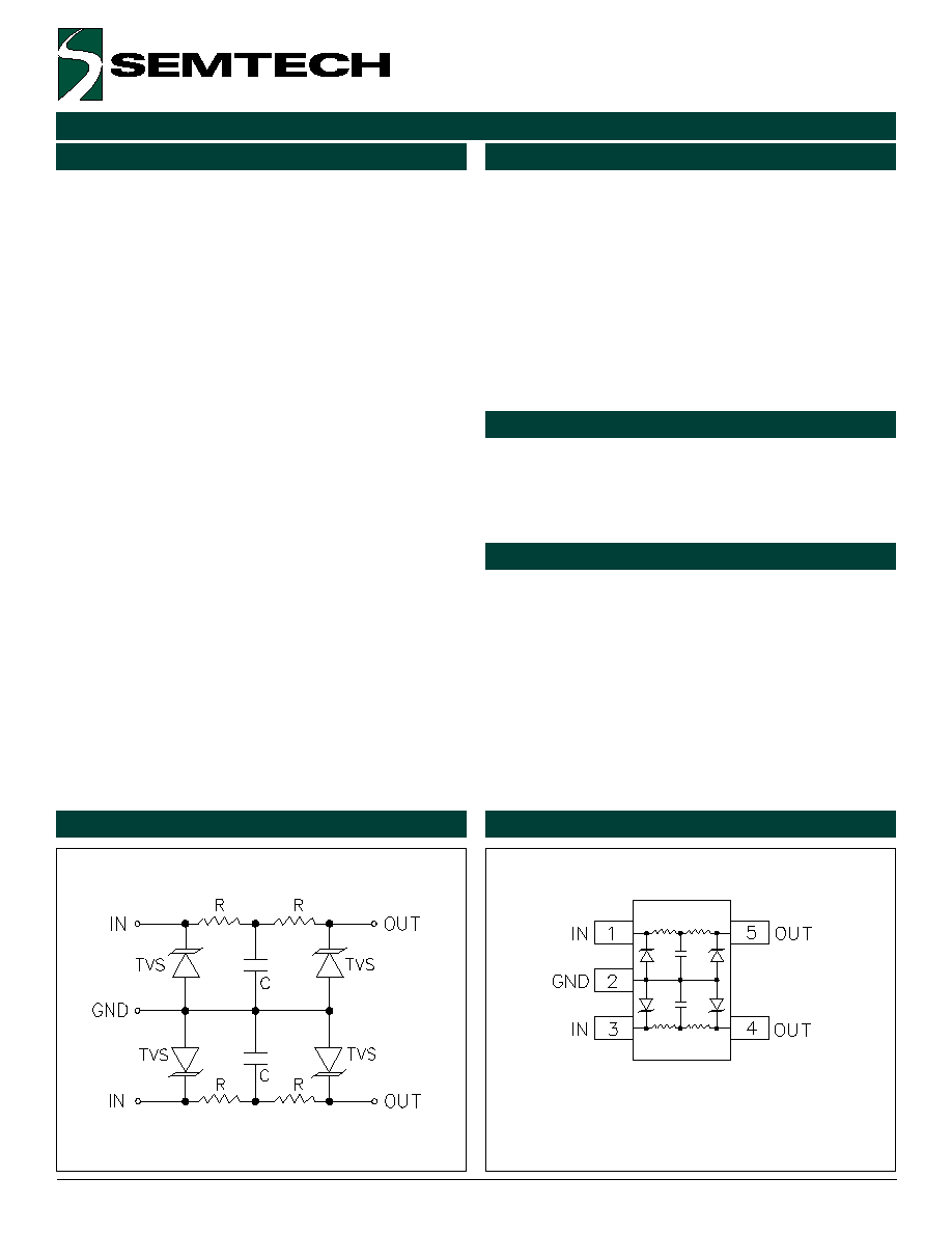
Circuit Diagram
Schematic & PIN Configuration
Revision 9/2000
The STF701 is a low pass T-filter with integrated TVS
diodes. It is designed to provide bi-directional un-
wanted EMI/RFI signals filtering and electrostatic
discharge (ESD) protection in portable electronic
equipment. Each device will provide filtering and
protection for two I/O lines.
The STF701 is constructed using thin-film-on-silicon
technology. The device has very low insertion loss in
the pass band (to approximately 10MHz) and good
attenuation at high frequencies (approximately
100MHz to 1GHz). Each line features two stages of
TVS diode protection. The TVS diodes provide effec-
tive suppression of ESD voltages in excess of 15kV (air
discharge) and 8kV (contact discharge) per IEC 61000-
4-2, level 4.
The clamping characteristics of the device are opti-
mized by the use of two TVS diodes. The TVS diodes
serve a dual purpose of protecting the internal capaci-
tor and the sensitive IC connected to the line. The
voltage divider action of the circuit means the voltage
across the protected IC will be very close to the break-
down voltage (V
BR
) of the second TVS.
The small size and integrated feature of the STF701
minimizes required board space and increases system
reliability. The STF701 is suitable for use in portable
communications devices such as cellular handsets and
accessory kits.
Applications
Mechanical Characteristics
u
Cell phone handsets
u
Cell phone accessories
u
RF Communications equipment
u
Laptop Computers
u
Two-way pagers
u
GPS Devices
u
Bidirectional EMI/RFI filtering with integrated ESD
protection
u
ESD protection to IEC 61000-4-2 Level 4
u
Filtering and ESD protection for two data lines
u
Low insertion loss to 10MHz
u
Good attenuation of high frequency signals
u
Low TVS operating voltage (5V)
u
Low clamping voltage
u
Low leakage current
u
Thin-film-on-silicon technology
u
EIAJ SC70-5L package
u
Molding compound flammability rating: UL 94V-0
u
Marking : 701
u
Packaging : Tape and Reel per EIA 481
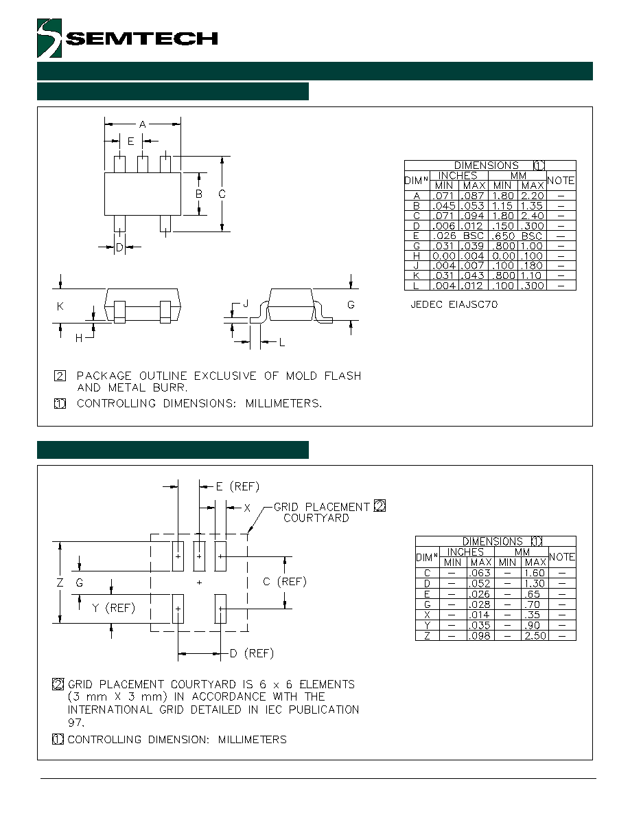
SC70-5L (Top View)
4
� 2000 Semtech Corp.
www.semtech.com
PROTECTION PRODUCTS
STF701
Figure 1 - STF701 Circuit Diagram
Figure 2 - STF701 Connection Diagram
Device Connection for Protection of Two Data Lines
The STF701 is designed to provide EMI filtering and
ESD protection for two I/O lines. The equivalent circuit
diagram is shown in Figure 1. The device is connected
as follows:
1. Line 1 is connected at pins 1 & 5 and line 2 is
connected at pins 3 & 4 (Figure 2). The device is
symmetrical so input & output connections can be
made on either side of the device. Pin 2 is con-
nected to ground. The ground connection should
be made directly to the ground plane for best
results. The path length is kept as short as pos-
sible to reduce the effects of parasitic inductance
in the board traces.
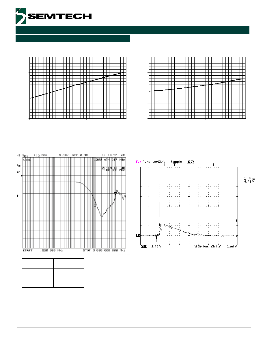
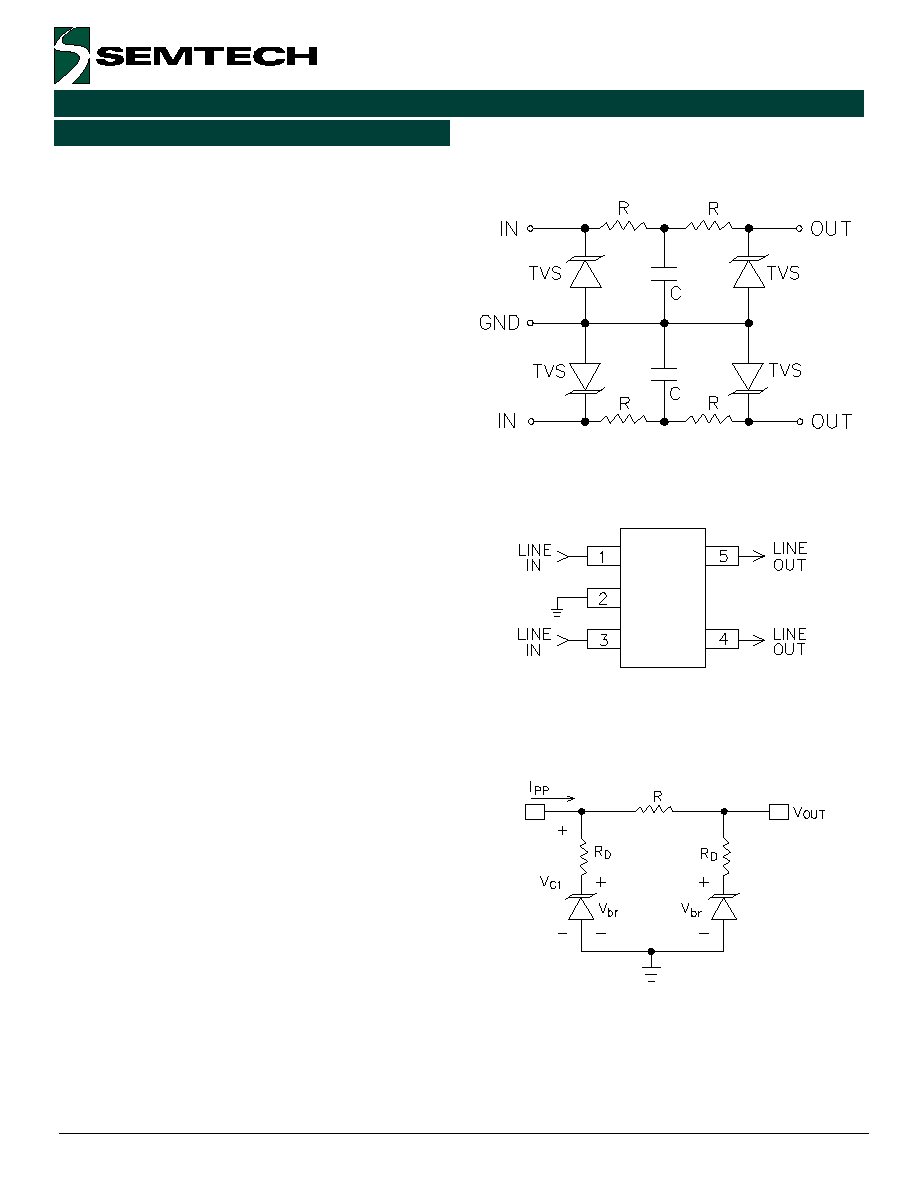
Voltage Clamping Characteristics.
The clamping characteristics of the STF701 are opti-
mized by the use of two TVS diodes in the protection
circuit (Figure 3). An ESD strike on the protected line
will be initially suppressed by the first TVS diode. The
voltage across the TVS will be the clamping voltage of
the device (V
C1
) given by:
V
C1
= V
br
+ R
D
* I
PP
where
V
br
= Breakdown voltage of the TVS
R
D
= Dynamic resistance of the TVS
I
PP
= Peak pulse (ESD) current
The dynamic resistance of the TVS is very small,
typically < 0.5W.
The second TVS will be subjected to V
C1
through the
voltage divider formed by the series resistor (R) and
the dynamic resistance of the TVS. Since R >> RD
then by the voltage divider theorem, the voltage seen
by the protected IC will be a few millivolts above the
breakdown voltage (V
br
) of the second TVS.
Figure 3 - STF701 Clamping Characteristics
Applications Information