
SPICoder
TM
UR5HCSPI
Zero-Power
TM
Keyboard Encoder &
Power Management IC for H/PCs
SPICoder is a trademark of Semtech Corp. All
other trademarks belong to their respective
companies.
Copyright Semtech 1997-2001
DOC5-SPI-DS-117
www.semtech.com
1
HID & SYSTEM MANAGEMENT PRODUCTS, H/PC IC FAMILY
DESCRIPTION
FEATURES
∑ StrongARM
TM
Handheld PCs
∑ Windows CE
Æ
Platforms
∑ Web Phones
∑ Personal Digital Assistants (PDAs)
∑ Wearable Computers
∑ Internet Appliance
The SPICoder
TM
UR5HCSPI
keyboard encoder and power
management IC is designed
specifically for handheld PCs
(H/PCs). The off-the-shelf
UR5HCSPI will readily work with
CPUs designed for Windows CE
Æ
,
saving OEMs significant
development time and money as
well as minimizing time-to-market for
the new generations of handheld
products.
Three main design features of the
UR5HCSPI make it the ideal
companion for the new generation
of Windows CE
Æ
-compatible,
single-chip computers: low-power
consumption; real estate-saving
size; and special keyboard modes.
"Quasi" Zero-Power
TM
consumption
(less than 2µA @ 3V), a must for
H/PCs, provides the host system
with both power management and
I/O flexibility, with almost no battery
drainage.
Finally, special keyboard modes
and built-in power management
features allow the SPICoder
TM
to
operate in harmony with the power
management modes of Windows
CE
Æ
, resulting in more user flexibility
and longer battery life.
The UR5HCSPI also offers
programmable features for wake-up
keys and general purpose I/O pins.
∑ Compatible with "system-on silicon"
CPUs for H/PCs
∑ Special keyboard and power
management modes for H/PCs,
including programmable "wake-up"
keys
∑ Scans, debounces, and encodes
an 8 x 12 matrix and controls
discrete switches and LED
indicators
∑ Custom versions available
∑ SPI-compatible keyboard encoder
and power management IC with
other interfaces available
∑ Compatible with Windows CE
Æ
keyboard specification
∑ Zero-Power
TM
-- typically
consuming less than 2µA,
between 3-5V
∑ Offers overall system power
management capabilities
1
11
12
22
33
23
44
34
_PWR_OK
NC0
OSCO
OSCI
Vcc
NC
NC
_RESET
_WKU
Vx
C7
_ATN
_SS
SCK
MOSI
MISO
XSW
SW0
C8
C9
C10/WUKO
C11/_LID
NC
LED2
LED1
LED0
_IOTEST
Vss
NC
R7
R6
R5
R4
C6
C5
C4
C3
C2
C1
C0
R0
R1
R2
R3
QFP
UR5HCSPI-FB
C6
C7
Vx
NC
_WKU
_RESET
Vcc
OSCI
OSCO
NC0
NC
C5
C4
C3
C2
C1
C0
R0
R1
R2
R3
R4
_PWR_OK
_ATN
_SS
SCK
MOSI
MISO
XSW
SW0
C8
C9
C10/WUKO
NC
R5
R6
R7
Vss
NC
_IOTEST
LED0/GIO0
LED1/C13
LED2/C12
C11/_LID
40
1
6
7
12
17
18
23
28
29
34
39
UR5HCSPI-FN
PLCC
APPLICATIONS
PIN ASSIGNMENTS
Package Options
Pitch in mm's
TA=-20∞ C to +85∞ C
44-pin, Plastic PLCC
1.27 mm
UR5HCSPI-XX-FN
44-pin, Plastic QFP
0.8 mm
UR5HCSPI-XX-FB
Other Materials
Type
Order number
SPICoder
TM
Testing Board
ASY5-SPI-XXX
Note 1: XX=Optional Customization, XXX= Denotes Revision number
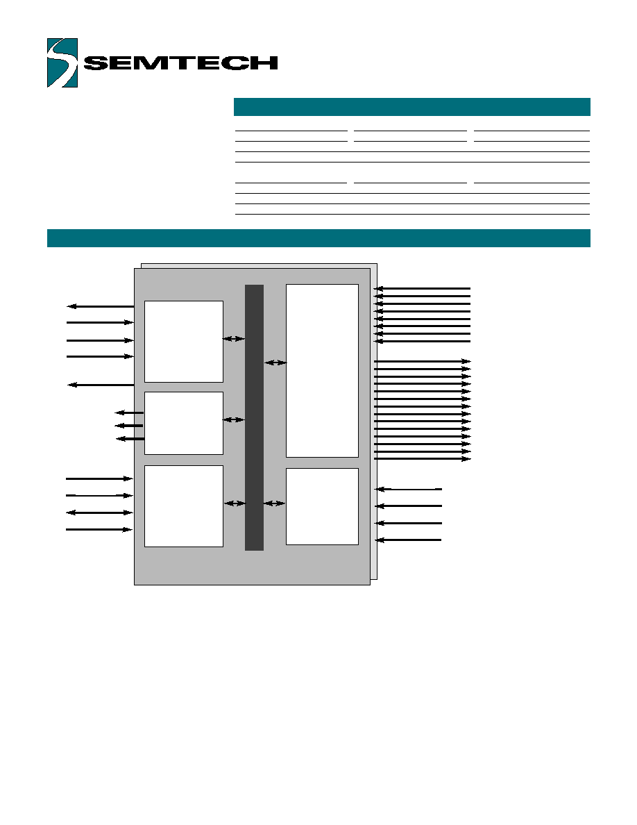
BLOCK DIAGRAM
ORDERING CODE
Copyright Semtech 1997-2001
DOC5-SPI-DS-117
www.semtech.com
2
Keyboard
Scanner
&
Keyboard
State
Control
R0-R8
SPI
Communication
Channel
C0-C11
Keyboard
Matrix
LID Latch Monitor
Wake-Up Keys Only Signal
Switch External to Case
Switch
System
Monitor
Input
Signals
Power
Management
Unit
LEDs
LID
WUKO
XSW
SWO
PWR_OK
WKUP
IOTEST
WKU
MISO
MOSI
SCK
SS
ATN
UR5HCSPI
LED0
LED1
LED2

FUNCTIONAL DESCRIPTION
PIN DEFINITIONS
Copyright Semtech 1997-2001
DOC5-SPI-DS-117
www.semtech.com
3
The UR5HCSPI consists
functionally of five major sections
(see the Functional Diagram on
page 2). These are the Keyboard
Scanner and State control, the
Programmable I/O, the SPI
Communication Channel, the
System Monitor and the Power
Management unit. All sections
communicate with each other and
operate concurrently.
Mnemonic PLCC QFP
Type Name and Function
VCC
44
38
Power Supply: 3-5V
VSS
22
17
I
Ground
VX
4
43
I
Tie to VCC
OSCI
43
37
I
Oscillator input
OSCO
42
36
O
Oscillator output
_RESET
1
41
I
Reset: apply 0V to provide orderly
start-up
MISO
34
29
O
SPI Interface Signals
MOSI
35
30
I
SCK
36
31
I
_SS
37
32
I
Slave Select: If not used tie to VSS
_IOTEST
24
18
O
Wake-Up Control Signals
_WKU
2
42
I
R0-R4
13-17
8-12
I
Row Data Inputs
R5-R7
19-21
13-15
I
Port provides internal pull-up resistors
C0-C5
12-7
7-2
O
Column Select Outputs:
C6-C7
6-5
1,44
O
C8-C9
31-30
26-25
O
Multi-function pins
C10/WUKO
29
24
I/O C10 & "Wake-Up Keys Only" imput
C11/_LID
28
23
I/O C11 & Lid latch detect input
Miscellaneous functions
LED2
27
21
I/O LED2 output
LED1
26
20
I/O LED1 output
LED0
25
19
I/O LED0 output
XSW
33
28
I
External discrete switch
SWO
32
27
I
Discrete switch
Power Management Pins
_ATN
38
33
O
CPU Attention Output
_PWR_OK
39
34
I
Power OK Input
NC
3,18
39-40
No Connects: these pins are unused
23,40
16,22
NC0
41
35
NC0 should be tied to VSS or GND
Note 1: An underscore before a pin mnemonic denotes an active low signal.

PIN DESCRIPTIONS
Copyright Semtech 1997-2001
DOC5-SPI-DS-117
www.semtech.com
4
VCC and VSS
VCC and VSS are the power
supply and ground pins. The
UR5HCSPI will operate from a 3-5
Volt power supply. To prevent noise
problems, provide bypass
capacitors and place them as
close as possible to the IC with the
power supply. VX, where available,
should be tied to Vcc.
OSCI and OSCO
OSCI and OSCO provide the input
and output connections for the on-
chip oscillator. The oscillator can
be driven by any of the following
circuits:
- Crystal
- Ceramic Resonator
- External Clock Signal
The frequency of the on-chip
oscillator is 2 MHz.
_RESET
A logic zero on the _RESET pin will
force the UR5HCSPI into a known
start-up state. The reset signal can
be supplied by any of the following
circuits:
- RC
- Voltage monitor
- Master system reset
MOSI, MISO, SCK, _SS, _ATN
These five signals implement the
SPI interface. The device acts as a
slave on the SPI bus. The _SS
(Slave Select) pin should be tied to
ground if not used by the SPI
master. The _ATN pin is asserted
low each time the UR5HCSPI has a
packet ready for delivery. For a
more detailed description, refer to
the SPI Communication Channel
section on page 9.
_IOTEST and _WKU
"Input Output Test" and "Wake Up"
pins control the stop mode exit of
the device. The designer can
connect any number of active low
signals to these two pins through a
17K resistor, in order to force the
device to exit the stop mode. A
sample circuit is shown on page 15
of this document.
All the signals are "wire-anded."
When any one of these signals is
not active, it should be floating (i.e.,
these signals should be driven from
"open-collector" or "open-drain"
outputs). Other configurations are
possible; contact Semtech.
R0-R 7
The R0-R7 pins are connected to
the rows of the scanned matrix.
Each pin provides an internal pull-
up resistor, eliminating the need for
external components.
C0-C9
C0 to C9 are bi-directional pins
connected to the columns of the
scanned matrix. When a column is
selected, the pin outputs an active
low signal. When the column is de-
selected, the pin turns into high-
impedance.
C10/WUKO
The C10/WUKO pin acts
alternatively as column scan output
and as an input. As an input, the
pin detects the "Wake-Up Keys
Only" signal, typically provided by
the host CPU to indicate that the
user has turned the unit off. When
the device detects an active high
state on this pin, it feeds this
information into the "Keyboard State
Control" unit, in order to disable the
keyboard and enable the
programmed wake-up keys.
C11/_LID
The C11/_LID pin acts in a similar
manner to the C10/WUKO. This pin
is typically connected to the LID
latch through a 150K resistor, in
order to detect physical closing of
the device cover. When the pin
detects an active low state in this
input, it feeds this information into
the "Keyboard State Control" unit, in
order to disable keys inside the
case and enable only switches
located physically on the outer
body of the H/PC unit.
LED0, LED1 and LED2
These three pins provide an active
low drive for LED indicators. The
programming of these pins is
explained in the LEDs section on
page 8 of this document.
PIN DESCRIPTIONS, (CON'T)
THE WINDOWS CE
Æ
KEYBOARD
Copyright Semtech 1997-2001
DOC5-SPI-DS-117
www.semtech.com
5
XSW
The XSW pin is dedicated to an
external switch. This pin is
handled differently than the rest of
the switch matrix and is intended
to be connected to a switch
physically located on the outside of
the unit.
SW0
The SW0 pin is a dedicated input
pin for a switch.
PWR_OK
The PWR_OK is an active low pin
that monitors the battery status of
the unit. When the UR5HCSPI
detects a transition from high to
low on this pin, it will immediately
enter the STOP mode, turn the LED
off and remain in this state until the
batteries of the unit are replaced
and the signal is deasserted.
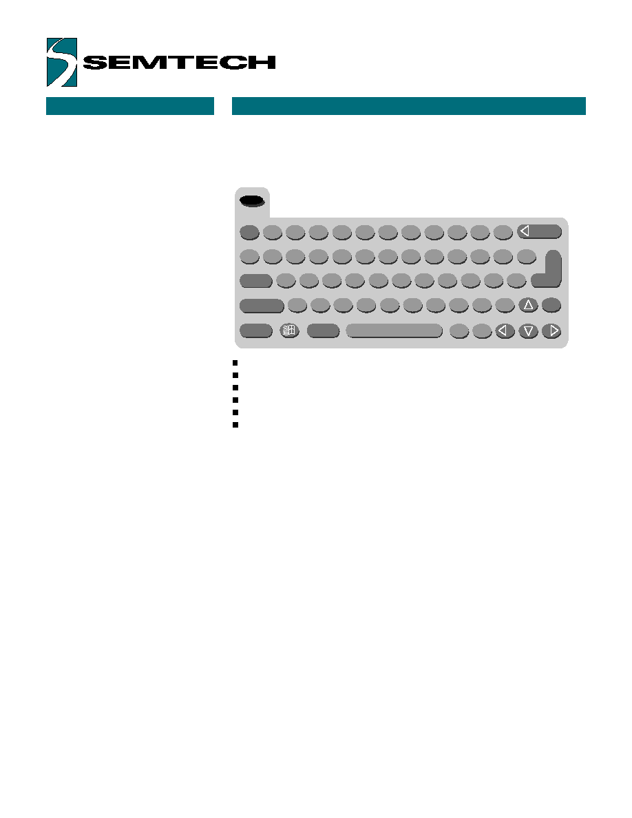
The following illustration shows a typical implementation of a Windows CEÆ
keyboard.
Windows CEÆ does not support the following keyboard keys typically
found on desktop and laptop keyboards:
INSERT
SCROLL LOCK
PAUSE
NUM LOCK
Function Keys (F1-F12)
PRINT SCREEN
If the keyboard implements the Windows key, the following key
combinations are supported in the Windows CE
Æ
environment:
Key Combination
Result
Windows
Open Start Menu
Windows+K
Open Keyboard Tool
Windows+I
Open Stylus Tool
Windows+C
Open Control Panel
Windows+E
Explore the H/PC
Windows+R
Display the Run Dialog Box
Windows+H
Open Windows CEÆ Help
Ctrl+Windows+A
Select all on desktop
1 !
esc
3 #
2 @
5 %
4 $
7 &
6 ^
9 (
8 *
-
_
0 )
E
W
T
R
U
Y
O
I
P
Q
F
D
H
G
K
J
L
S
A
V
C
N
B
M
X
Z
tab
shift
ctrl
shift
enter
= +
\ |
' "
; :
. >
, <
/ ?
`
~
] }
[ {
power
alt