
Cool Solutions for Wireless Connectivity
XEMICS SA
∑
e-mail: info@xemics.com
∑
web: www.xemics.com
Datasheet XE1218A: Low
Power single die FM receiver
XE1218A
Low power single die FM receiver
General Description
The XE1218 is a single die, low power, FM
receiver operating in the VHF band from 130MHz
to 230MHz. Its highly integrated architecture allows
for RF and audio functions on the same die, whilst
minimizing the external components needed to
build a complete application at the same time.
The XE1218A enables single chip, complete audio
transmission solutions, where the antenna feeds
the incoming RF signal directly into the XE1218A
and an amplified audio signal can be fed to an
earphone directly from the XE1218A's output.
Flexibility has been built into the XE1218A: various
different transmission channels can be selected,
the audio output can also be fed to a post
processing circuit such as sound de-emphasis or
an external power amplifier.
The XE1218A is optimized for battery powered
applications, it can be operated directly on one
lithium 1.5V battery cell.
Applications
∑ Wireless phone headset
∑ Local area voice paging
∑ FM broadcasting miniature receiver
∑ Toys
Main features
∑ Tuneable from 130MHz to 230 MHz
∑ High reception sensitivity: -100dBm
∑ Integrated RF filtering
∑ Low voltage operation: down to 1.1V
∑ Low power consumption: typical 2.5mA
∑ 6 kHz audio bandwidth
∑ 40 dB audio SNR
∑ Integrated earphone audio amplifier
∑ Line out for external audio amplifier
∑ Mute function
Ordering Information
Part Number
Temperature range
Package
XE1218AS000BF
-10∞C to 40∞C
Bare die
LNA
FM
DEMOD
Audio
SW
AFC
OSC
PA
VDD
VCCR VCCA
VM VSS
RFI
RFG
RFT
LOP LON XP XN
EAR
VOL
OUT
VCCO
AUD

2
D0204-157
Datasheet XE1218A: Low
Power single die FM receiver
Table of Contents
1. Functional description
3
1.1General description
3
1.2RF front end
3
1.3Audio stage
3
2. Functional implementation
4
2.1 Block diagram
4
2.2 Operation overview
4
2.3 Application example
5
3. Electrical characteristics
5
3.1 Absolute maximum ratings
5
3.2 Recommended operating conditions and electrical specifications
5
4. Interconnections
6
4.1 Bare die pad out
6
4.2 Pad coordinates
7
4.3 XE1218A packaging
7
4.4 TQFP44 pin-out
8
5. Input ≠ output signal description
9
6. Application information
10
6.1 Recommended crystal oscillator
10
6.2 Using a low impedance audio output
10
6.3 Using the high impedance line out OUT
10
6.4 Recommended antenna
11

3
D0204-157
Datasheet XE1218A: Low
Power single die FM receiver
1. Functional description
1.1
General description
The XE1218A is an integrated FM receiver including all the necessary functions to process a modulated RF
signal at its input and deliver a "speech quality" audio signal at its output. The XE1218A was designed for
maximum system simplicity thus it requires only 12 external components to offer antenna in, audio out
functionality. The XE1218A also offers design flexibility. A direct connection to an earphone is possible through
the pin EAR, this takes advantage of the internal audio power amplifier or an external audio amplifier, or an
audio processing device can be connected via the OUT (line out) pin.
1.2
RF front end
The FM signal received through the antenna is delivered to an integrated LNA via an external matching circuit.
A low IF architecture is implemented to down-convert the incoming signal to an intermediate frequency (IF) of
25kHz. This IF signal is then filtered to remove any DC components and equalized to offer a clean digital signal
to the demodulator. The FM demodulator uses digital delay line architecture to convert the signal to a pulse
width modulated signal at twice the IF frequency. The XE1218A has an integrated AFC which is used for the
demodulator to have its clock frequency track the IF frequency.
1.2.1
LNA
The noise figure (NF) for this block is less than 6dB, for an antenna impedance in the 1 to 2 k range. Out of
the 6dB, 3dB is due to the noise of the image frequency that is not rejected. The sensitivity is ≠100dBm
(SINAD=10 dB, fdev = 3kHz).
1.2.2
Mixer, down-conversion
The down-conversion is implemented as a Gilbert cell. This implementation uses low IF and does not have
provisions for integrated image rejection. The incoming audio channel will be demodulated at F
lo
= F
IN
≠ 25kHz.
This is to say that the image frequency will be located at F
IN
≠ 50kHz and will not be attenuated by the
XE1218A's RF receiving circuitry. For multi-channel operation within reception range of several XE1218A
receivers, it is recommended that the various carrier frequencies be spaced by at least 100kHz, better yet
200kHz.
1.2.3
DC offset cancellation, IF amplifier chain
DC components are attenuated in an off-set cancellation block. An on-chip low pass filter provides attenuation
greater than 65dBm measured F
IF
+ 100kHz
1.2.4
Demodulation and AFC circuitry
The demodulator converts the signal from the IF amplifier into a pulse width modulated signal at twice the IF
frequency. A follow-on block generates the AFC to track the IF frequency. Proper tracking of the IF frequency is
necessary for the stability of the RF link as the XE1218A operates in narrow band mode.
1.2.5
Crystal and local oscillator
The local oscillator provides the XE1218A's down-converter mixer with the proper frequency: F
lo
. It is
implemented with a crystal oscillator working on the external crystal's overtone harmonic.
1.3
Audio stage
1.3.1
Audio processing
The XE1218A integrated audio processing circuitry filters the input pulse width modulated (PWM) signal from
the demodulator and provides for two different output feeds. All necessary bias currents and voltages for this
analog block are on-chip, including a voltage multiplier circuit. When the incoming RF signal becomes low, the
signal to noise ratio at the audio output decreases, which drastically reduces the sound quality and intelligibility.
For user convenience, a mute function is implemented in the audio section. When the signal to noise ratio at the
output is too low (typ. 10 to 15 dB) the audio output is shut down.
4
D0204-157
Datasheet XE1218A: Low
Power single die FM receiver
1.3.2
Audio output stage
An integrated power amplifier (PA) allows for a direct connection to an earphone. Controlled by an external
potentiometer (100k) a maximum attenuation of 10dB is achievable on the EAR output, 21.5dB with 1M. A
high impedance line out (10k) is available through the pad OUT.
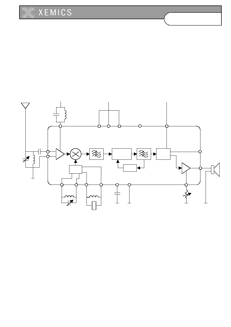
2. Functional implementation
2.1 Block diagram
2.2 Operation overview
While the XE1218A is a single channel receiver, various fixed frequencies can be selected between 130MHz
and 230MHz. This is achieved by changing the external RF front-end components: L1, L2, L3, L4, C1, C2, C4,
C5 and Xtal. The XE1218A FM receiver connects to the antenna via a differential input: pins RFI and RFG. The
external components L4, C4 and C5 must tune the circuit to the incoming carrier frequency. L2 and C2 are
calculated to tune the oscillator to the desired incoming carrier frequency. Xtal is selected according to the
desired input carrier frequency, L3 relaxes the oscillator's Q factor to insure greater reception stability.
Reception sensitivity is determined through the LNA's external tank circuit: C1 and L1.
Two types of audio outputs can be selected: OUT (line out, 10k output impedance) to connect to an external
audio processing circuit or amplifier and EAR for direct connection to an earphone. An external R1 is used to
adjust the volume through pin VOL. The internal RF and audio blocks each have their own supply voltage as
well as a common VDD. Clean voltage must be supplied to each of these supplies (VCCR, VCCA, VCCO and
VDD).
Xtal
XE1218
LNA
FM
DEMOD
Audio
SW
AFC
OSC
PA
VCC
Line OUT
VDD
VCCR VCCA
VCC
VM VSS
L2
C2
C1 L1
C5
R1
Volume
Control
C3
RFI
RFG
RFT
LOP LON XP XN
EAR
VOL
OUT
VCCO
VCC
L3
A1
L4
AUD
C4
5
D0204-157
Datasheet XE1218A: Low
Power single die FM receiver
2.3 Application example
To tune the above circuit to a carrier frequency of 160.325MHz, the following external components must be
implemented:
L1
56nH-5%
C1
12pF-5%
C5
2pF - 6pF-5%
L2
56nH-5%
C2
10pF- 15pF-5%
R1
100k - 10%
L3
180nH-5%
C3
10nF-5%
Xtal
160.325MHz
L4
120nH ≠ 5%
C4
22pF-5%
A1
Wire l > 40mm
The value of the capacitors given here may change slightly for different PCBs.
3. Electrical characteristics
3.1 Absolute maximum ratings
Parameter
Min
Max
Supply voltage
-0.3V
2.5V
Storage Temperature
-55∞C
+125∞C
Stress beyond those listed under absolute maximum ratings may cause permanent damage to the XE1218
device. These are stress ratings only, and functional operation of the device at these or any other condition
beyond those under "recommended operating conditions" is not implied. Exposure to "absolute maximum
ratings" conditions for extended periods may affect the device reliability.
3.2 Recommended operating conditions and electrical specifications
General conditions: Temp = 25∞C, VDD= 1.3V, Carrier Frequency=160MHz, unless otherwise specified
Symbol
Description
Condition
Min
Typ.
Max
Unit
Electrical supply parameters
VDD
Power supply
1.1
1.3
1.6
V
IDD
Supply current
Receiver ON, without
earphone PA enabled
2.5
4.5
mA
TEMP
Operating temperature range
-10
+40
∞C
Radio Frequency parameters
RF-IN
Carrier frequency
Input range
130
230
MHz
F-DEV
Deviation frequency
Maximum deviation of the
incoming modulated signal
8
kHz
LO-D
Local Oscillator shift
Crystal ageing and
temperature drift not
accounted for
±20
ppm
RFS
RF input sensitivity
f
modulated
= 1kHz, f
dev
= 3kHz
-100
dBm
ACR
Adjacent channel
rejection
f
unwanted
= f
Rfin
+ 100kHz
f
modulated
= 1kHz, f
dev
= 3kHz
P
in
= RFS + 10dBm
SINAD = 10dB
50
dB
Audio parameters
AOB
Audio Output
bandwidth (typical)
Fdev = 3kHz
0.1
6
kHz
AOD
Audio distortion on
PA output (EAR)
Only relevant if using the
direct earphone connection
f
modulated
= 1kHz, f
dev
= 5kHz
R
vol
= 100k
P
in
= -60dBm, BW = 20kHz
2
8
%