 | –≠–ª–µ–∫—Ç—Ä–æ–Ω–Ω—ã–π –∫–æ–º–ø–æ–Ω–µ–Ω—Ç: XE3006 | –°–∫–∞—á–∞—Ç—å:  PDF PDF  ZIP ZIP |
Document Outline
- Table of contents
- 1 Device Description
- 2 Functional Description
- 3 Serial Communications
- 4 Sandmaní Function (XE3006)
- 5 Specifications
- 6 Application Information
- 7 Register Description
- 8 Mechanical Information
- 9 XE3005 Land pattern recommendations (5x4 uCSPÆ)
Cool Solutions for Wireless Connectivity
XEMICS SA
∑
e-mail: info@xemics.com
∑
web: www.xemics.com
Datasheet
XE3005/XE3006
XE3005 / XE3006
Low-Power Audio CODEC
General Description
The XE3005 is an ultra low-power CODEC (Analog
to Digital and Digital to Analog Converter) for voice
and audio applications. It includes microphone
supply, preamplifier, 16-bit ADC, 16-bit DAC, serial
audio interface, power management and clock
management for the ADC and the DAC. The
sampling frequency of the ADC and of the DAC
can be adjusted from 4 kHz to 48 kHz.
The XE3006 also includes the SandmanTM
function, which signals whether a relevant voice or
audio signal is present for the ADC or DAC.
Applications
∑ Wireless
Headsets
∑ BluetoothTM
headset
∑ Hands-free
telephony
∑
Digital hearing instruments
∑
Consumer and multimedia applications
∑
All battery-operated portable audio
devices
Features
∑ Ultra low-power consumption, below 2 mW
∑ Low-voltage operation down to 1.8 V
∑ SandmanTM function to reduce system
power consumption (XE3006)
∑ Single supply voltage
∑ Adjustable sampling frequency: 4 ≠ 48 kHz
∑ Digital format: 16 bit 2s complement
∑ Requires a minimum number of external
components
∑ Easy interfacing to various DSPs
∑ Direct connection to microphone and
speaker
∑ Various programming options
Quick Reference Data
∑ supply voltage
1.8 ≠ 3.6 V
∑ current (@20 kHz sampling) 0.4 mA
∑ sampling frequency
4 ≠ 48 kHz
∑ Typical dynamic range ADC
78 dB
∑ Typical dynamic range DAC
78 dB
Ordering Information
Part Package Ext.
part
no.
Temperature
range
XE3005
TSSOP 20 pins
XE3005I033
-20 to 70
∞ C
XE3005
uCSPÆ 20 balls
XE3005I064LF
-20 to 70
∞ C
XE3006
TSSOP 24 pins
XE3006I019
-20 to 70
∞ C
Amp.
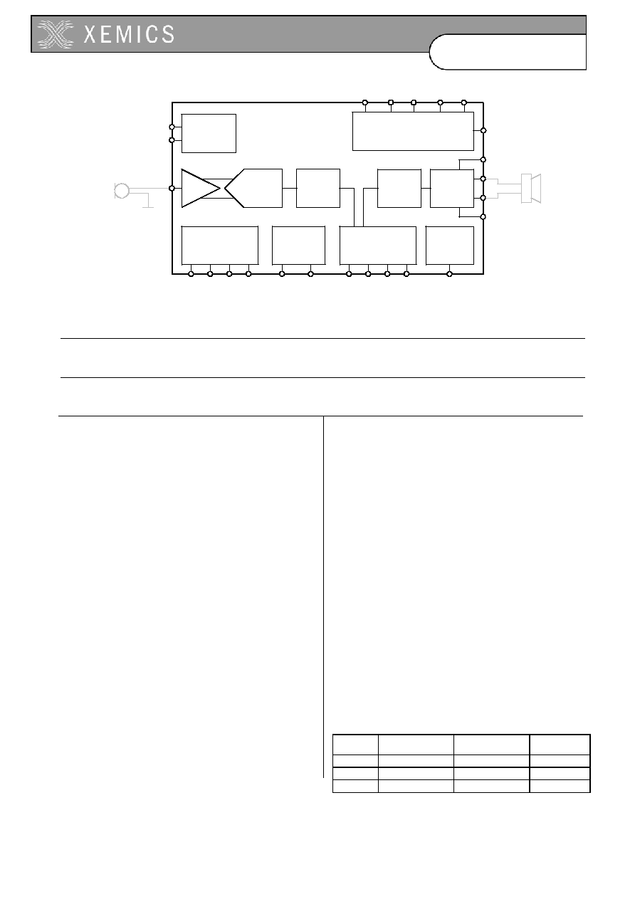
modulator
Decimator
Serial Audio
Interface
SPI
XE3006
Power supply
management
VDD
VSSD VREF
MCLK
BCLK FSYNC
SDI
SCK
SS
AIN
Microphone
Bias
VREG16
VSSA
Clock
mgt
PWM
DAC
Power
amplifier
AOUTP
AOUTN
VDDPA
VSSPA
SDO
MOSI
MISO
Sandman
Functions
SMDA
SMAD
RESET
VREG11
VSSA

2
D0311-116
Datasheet
XE3005/XE3006
Table of contents
1
Device Description...................................................................................................................................... 3
1.1
Terminals Description XE3005/6 .................................................................................................................. 4
2
Functional Description ............................................................................................................................... 5
2.1
Device Functions .......................................................................................................................................... 5
2.2
Power-Down Functions............................................................................................................................... 12
3
Serial Communications ............................................................................................................................ 13
3.1
Serial Audio Interface.................................................................................................................................. 13
3.2
Register Programming................................................................................................................................ 14
3.3
Serial Peripheral Interface - SPI ................................................................................................................. 15
4
SandmanTM Function (XE3006)................................................................................................................ 17
5
Specifications............................................................................................................................................ 19
5.1
Absolute Maximum Ratings ........................................................................................................................ 19
5.2
Recommended Operating Conditions ........................................................................................................ 19
5.3
Electrical Characteristics ............................................................................................................................ 20
6
Application Information............................................................................................................................ 27
6.1
Application Schematics ≠ XE3006.............................................................................................................. 27
7
Register Description................................................................................................................................. 28
7.1
Register Functional Summary .................................................................................................................... 28
7.2
Register Definitions..................................................................................................................................... 29
8
Mechanical Information............................................................................................................................ 32
8.1
XE3005 package size (TSSOP20) ............................................................................................................. 32
8.2
XE3005 package size (5x4 uCSP
Æ
) ........................................................................................................... 33
8.3
XE3006 Package size (TSSOP24) ............................................................................................................. 34
9
XE3005 Land pattern recommendations (5x4 uCSP
Æ
) .......................................................................... 35
3
D0311-116
Datasheet
XE3005/XE3006
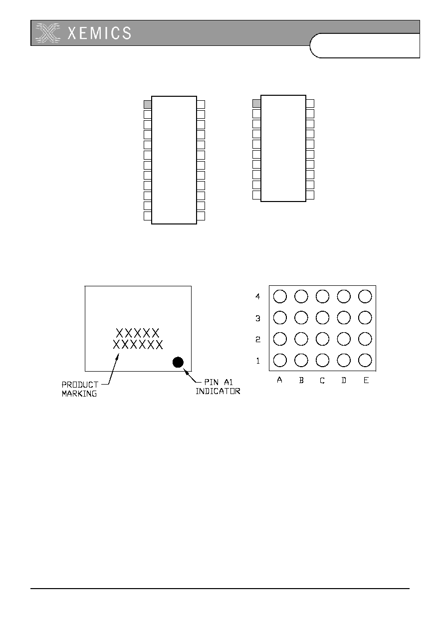
1 Device
Description
1
5
6
7
8
9
10
11
12
MCLK
SMAD
SMDA
VDD
NRESET
VSSA
VREG16
VREF
VSSA
VSSD
VREG11
AIN
24
23
22
21
20
19
18
17
16
14
13
MOSI
SS
SCK
MISO
SDI
SDO
BCLK
FSYNC
AOUTP
VDDPA
AOUTN
VSSPA
4
15
3
2
1
5
6
7
8
9
10
MCLK
SS
VDD
NRESET
VREG16
VREF
VSSA
VSSD
VREG11
AIN
20
19
18
17
16
15
14
13
12
MOSI
SCK
SDI
SDO
BCLK
FSYNC
AOUTP
VDDPA
AOUTN
VSSPA
4
11
3
2
XE3006
XE3005
Figure 1: Pin layout of the XE3006 and XE3005 in TSSOP
TOP VIEW
BOTTOM VIEW
XEMICS
XE3005
AOUTN
AOUTP
BCLK
SDI
SCK
VSSPA
VDDPA
FSYNC
SDO
MOSI
VSSD
VREG16
SS
MCLK
AIN
VSSA
VREF
NRESET
VDD
VREG11
Figure 2: Pin layout of the XE3005 in uCSPÆ
The XE3006 is available in a TSSOP24 package. The XE3005 is available in a TSSOP20 and uCSPÆ package.
Detailed information is found in chapter 8, Mechanical Information.
4
D0311-116
Datasheet
XE3005/XE3006
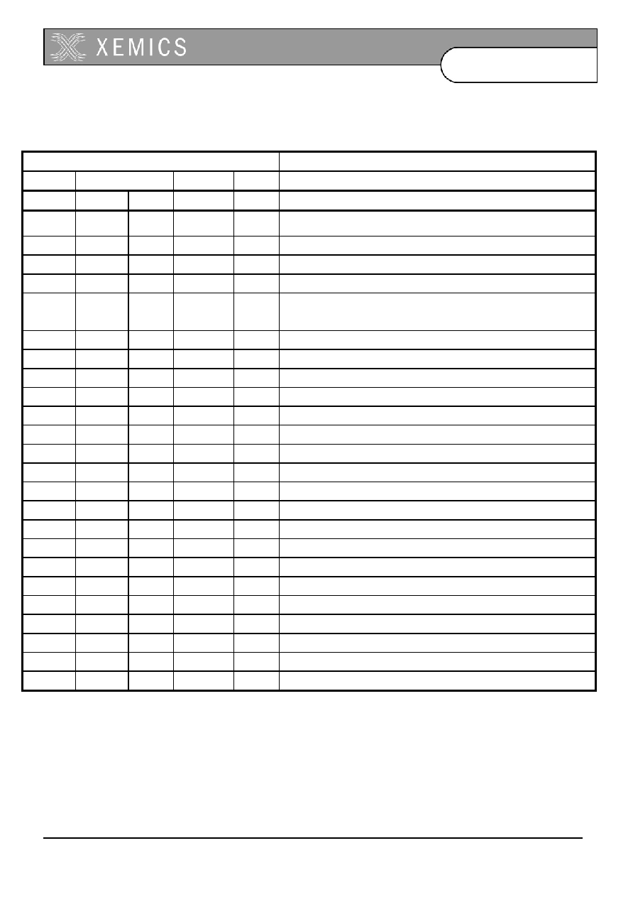
1.1 Terminals Description XE3005/6
Terminals
Description
XE3006 XE3005 Name
Type
1
TSSOP24 TSSOP20
uCSP
Æ
1 1
A2
MCLK
DI
Master Clock. MCLK derives the internal clocks of ADC and
DAC
2
N/A
N/A
SMAD
DO
Sandman output ADC
3
N/A
N/A
SMDA
DO
Sandman output DAC
4
3
A1
VDD
AI
Digital power supply
5 4
B1
NRESET
ZI/O
Reset signal generated by the CODEC. If required, the reset
signal can be applied externally to initialize all the internal
CODEC registers
6 N/A
N/A
VSSA
AI
Analog
ground
7
5
C2
VREG16
AO
Regulator voltage 1.6 V. Can be used to supply the microphone
8 6
C1
VREF
AO
Reference
voltage
9 7
D1
VSSA
AI
Analog
ground
10 8 D2
VSSD
AI
Digital
ground
11
9
E2
VREG11
AO
ADC Regulated microphone output supply voltage 1.1 V
12
10
E1
AIN
AI
ADC Analog input signal
13
11
E3
VSSPA
AI
DAC Power Amplifier Ground
14
12
E4
AOUTN
AO
DAC Analog Output negative
15
13
D3
VDDPA
AI
DAC Power Amplifier Supply
16
14
D4
AOUTP
AO
DAC Analog Output positive
17
15
C3
FSYNC
DI/O
Serial audio interface Frame Synchronization
18
16
C4
BCLK
DI/O
Serial audio interface Bit Clock
19
17
B3
SDO
ZO
Serial audio interface Data Output
20
18
B4
SDI
DI PD Serial audio interface Data Input
21
N/A
N/A
MISO
ZO
SPI Master In Slave Out
22
19
A4
SCK
DI PD SPI Serial Clock
23
2
B2
SS
DI PU SPI Slave Select
24
20
A3
MOSI
DI PD SPI Master Out Slave In
Note: (1)
AI = Analog Input
AO = Analog Output
DI = Digital Input
DO = Digital Output
DI/O = Digital In or Out
ZO = Hi Impedance or Output
PU = internal Pull Up
PD = internal Pull Down
ZI/O = Hi impedance In or Out
5
D0311-116
Datasheet
XE3005/XE3006
2 Functional
Description
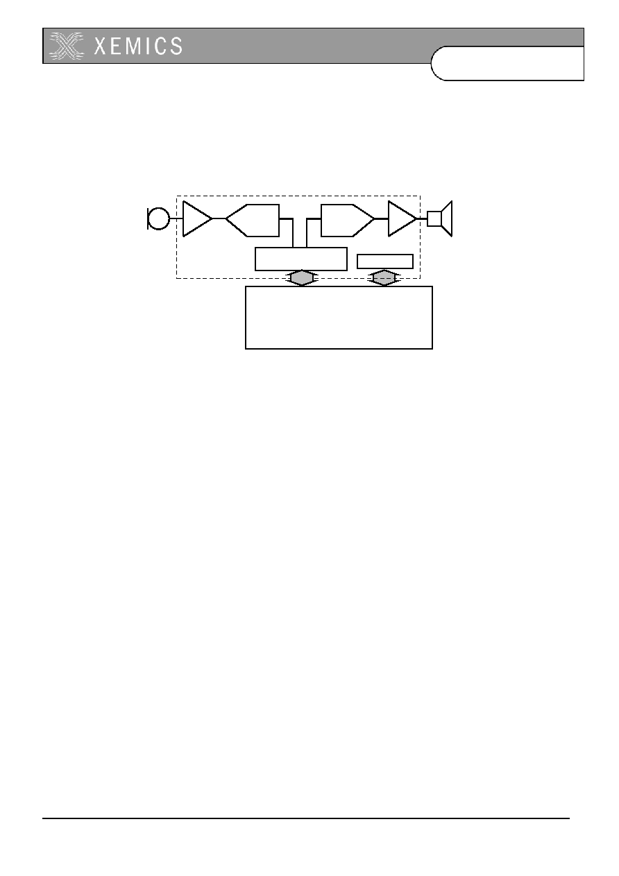
A CODEC is typically used for voice and audio applications as an interface between a Digital Signal processor
(DSP) or microcontroller and the analogue interfaces like a microphone and loudspeaker.
ADC
DAC
DSP / Microcontroller
Digital wireless transmission ≠ BluetoothTM
Voice recognition / speech synthesis
Power Amplifier
MIC-Amplifier
SPI
Serial Audio Interface
CODEC
Figure 3: typical usage of CODEC
This chapter provides a brief description of the CODEC features relating to the CODEC configuration. The
configuration of the CODEC is defined by programming registers through a serial interface. A detailed description
of the registers defining details of the CODEC setup can be found in chapter 3 and 7. Digital voice and audio
samples are passed through the Serial Audio Interface.
2.1 Device
Functions
2.1.1 ADC Signal Channel
The ADC channel is a chain of programmable amplifier, band-pass filter, sigma-delta modulator and a decimation
filter. The amplifier gain is programmable to 5x (default) and 20x. The band-pass filter has cut-off frequencies
proportional to the sampling rate. The sigma-delta modulator operates at a frequency of 64 times the sampling
rate. The analog modulator is followed by a digital decimation filter. The digital output data (16 bits, 2's
complement format) is made available through the Serial Audio Interface. The format of the Serial Audio interface
can be selected through register J.
With the default register settings the ADC can run at a sampling frequency up to 20 kHz. When used with a
sampling frequency higher than 20 kHz, then register C has to be changed.
The whole ADC chain can be powered-down through register I.