
∑
221 West Industry Court Deer Park, NY 11729 (631) 586 7600 FAX (631) 242 9798
∑
∑
World Wide Web Site - http://www.sensitron.com
∑
E-mail Address - sales@sensitron.com
∑
1
SENSITRON
SEMICONDUCTOR
TECHNICAL DATA
Data Sheet 4100 Rev. -
Three-Phase IGBT BRIDGE, With Gate Driver and Optical Isolation
DESCRIPTION: A 1200 VOLT, 120 AMP, THREE PHASE IGBT BRIDGE
ELECTRICAL CHARACTERISTICS PER IGBT DEVICE
(Tj=25
0
C UNLESS OTHERWISE SPECIFIED)
P
P
A
A
R
R
A
A
M
M
E
E
T
T
E
E
R
R
S
S
Y
Y
M
M
B
B
O
O
L
L
M
M
I
I
N
N
T
T
Y
Y
P
P
M
M
A
A
X
X
U
U
N
N
I
I
T
T
IGBT SPECIFICATIONS
Collector to Emitter Breakdown Voltage
I
C
= 2mA, V
GE
= 0V
BV
CES
1200
-
- V
Continuous Collector Current T
C
= 25
O
C
T
C
= 80
O
C
I
C
-
-
120
80
A
Pulsed Collector Current, 10mS
I
CM
-
-
180
A
Zero Gate Voltage Collector Current (For the module)
V
CE
= 1200 V, V
GE
=0V T
i
=25
o
C
V
CE
= 800 V, V
GE
=0V T
i
=125
o
C
I
CES
-
-
2
15
mA
mA
Collector to Emitter Saturation Voltage, T
C
= 25
O
C
I
C
= 80A, V
GE
= 15V, T
C
= 125
O
C
V
CE(SAT)
-
1.9
2.2
2.3 V
IGBT Internal Turn On Gate Resistance
30
Ohm
IGBT Internal Turn Off Gate Resistance
10
Ohm
IGBT Internal Soft Shutdown Turn Off Gate Resistance
100
Ohm
Short Circuit Time, Conditions TBD
10
usec
DC Bus Voltage Rate of Rise With 15V Supply Removed,
dv/dt
-
-
20
V/usec
Junction To Case Thermal Resistance
R
JC
- - 0.27
o
C/W
MODULE TOTAL WEIGHT
Estimated Total Weight
-
-
13
OZ
SPM6G120-120D

∑
221 West Industry Court Deer Park, NY 11729 (631) 586 7600 FAX (631) 242 9798
∑
∑
World Wide Web Site - http://www.sensitron.com
∑
E-mail Address - sales@sensitron.com
∑
2
SENSITRON
TECHNICAL DATA
Data Sheet 4100 Rev. -
Brake IGBT SPECIFICATIONS
Continuous Collector Current T
C
= 25
O
C
(Limited by Terminals) T
C
= 90
O
C
I
C
-
-
50
30
A
Pulsed Collector Current, 0.5mS
I
CM
-
-
100
A
IGBT Internal Gate Resistance
10
Ohm
IGBT Internal Gate Shunt Resistance
10
K Ohm
Junction To Case Thermal Resistance
R
JC
- - 0.35
o
C/W
ULTRAFAST DIODES RATING AND CHARACTERISTICS
Diode Peak Inverse Voltage
PIV
1200
-
-
V
Continuous Forward Current, T
C
= 90
O
C
I
F
-
-
80
A
Forward Surge Current, t
p
= 10 msec
I
FSM
-
-
200
A
Diode Forward Voltage, I
F
= 80A
V
F
-
1.8
2.3
V
Diode Reverse Recovery Time
(I
F
=80A, V
RR
=600V , di/dt < 1000 A/
µ
s)
t
rr
-
250
300
nsec
Maximum Thermal Resistance
R
JC
- - 0.45
o
C/W
MODULE STORAGE AND OPERATING CONDITIONS
Maximum operating Junction Temperature
T
jmax
-40
-
150
o
C
Maximum Storage Temperature
T
jmax
-55
-
150
o
C
Operating Altitude
-
-
50000
Ft
Vibration and shock requirements (1)
SPM6G120-120D

∑
221 West Industry Court Deer Park, NY 11729 (631) 586 7600 FAX (631) 242 9798
∑
∑
World Wide Web Site - http://www.sensitron.com
∑
E-mail Address - sales@sensitron.com
∑
3
SENSITRON
TECHNICAL DATA
Data Sheet 4100 Rev. -
Gate Driver
Supply Voltage, limits apply to Vcc, Vcc1, Vcc2, Vcc3
Vcc
12
15
18
V
Input On Current
HIN, LIN
2
5.0
8.0
mA
Opto-Isolator Logic High Input Threshold
I
th
- 1.6 2.0
mA
Input Reverse Breakdown Voltage
BV
in
5.0
-
-
V
Input Forward Voltage @ I
in
= 5mA
V
F
-
1.5
1.7
V
Under Voltage Lockout, limits apply to Vcc, Vcc1, Vcc2,
Vcc3
VCCUV 9.5
10.0
11.5 V
Internal Bootstrap Capacitor Value
10
-
-
uF
Desaturation Detection, High Input Threshold Voltage
7.0
8.0
9.0
V
Desaturation Detection, Low Input Threshold Voltage
6.0
7.0
8.0
V
Input-to-Output Turn On Delay
Output Turn On Rise Time
Input-to-Output Turn Off Delay
Output Turn Off Fall Time
at VCC=300V, IC=70A, T
C
= 25
t
ond
t
r
t
offd
t
f
-
-
-
-
800
100
1200
100
nsec
Dead Time Requirement, for Shoot Through Prevention
500
750
nsec
Opto-Isolator Input-to-Output Isolation Voltage, momentary
-
-
2500
-
V
Opto-Isolator Operating Input Common Mode Voltage
1000
V
Opto-Isolator Operating Input Common Mode Transient
Immunity, with Iin > 5mA
10
KV/usec
Pin-To-Case Isolation Voltage, DC Voltage
(Device will be tested at 3000V for 10 seconds)
-
2500
-
V
DC Bus Current Sensor (Bi-directional With Absolute Value Output)
Shunt Resistor Value
-
-
0.50
-
mOhm
Current Amplifier Gain, Referenced to Gnd1
0.025
V/A
Current Amplifier DC Offset (Zero DC Bus Current)
0
V
Over-Current Set Point
2.33
2.43
2.53
V
SPM6G120-120D

∑
221 West Industry Court Deer Park, NY 11729 (631) 586 7600 FAX (631) 242 9798
∑
∑
World Wide Web Site - http://www.sensitron.com
∑
E-mail Address - sales@sensitron.com
∑
4
SENSITRON
TECHNICAL DATA
Data Sheet 4100 Rev. -
+5V output, Isolated power supply
Referenced to Gnd1
4.75
5
5.25
V
Maximum load current
30
mA
+5V Input, Isolated power supply
(2)
Referenced to Gnd2
VDD 4.75
5
5.25
V
Base Plate Temperature
(2)
Base Plate Temperature Sensor Output Gain
Referenced to Gnd2
Tco
6.25
mV/
o
C
Temperature Sensor Output DC Offset
Referenced to Gnd2
424
mV
Accuracy, at temperature range from - 40
o
C to 125
o
C
-
+/-4.0
o
C
Phase A, Phase B, and Phase C Current Sensors (Bi-directional Output)
(2)
Current Amplifier Gain
Referenced to Gnd2
+/-
0.015
V/A
Current Amplifier DC Offset (Zero Phase Current)
Referenced to Gnd2
2.5
V
Current Amplifier Outputs Isolation To Phase Lines, and to
Gnd1
1500V
V
(1) Unit is designed to meet ....Vibration and Shock requirements, Mil-STD-810F shall be used. (514.5
and 516.5 methods respectively).
(2) Phase current sensors and base plate temperature sensor are floating sensors referenced to Gnd2. An
isolated 5V power supply shall be used to power these sensors.
SPM6G120-120D

∑
221 West Industry Court Deer Park, NY 11729 (631) 586 7600 FAX (631) 242 9798
∑
∑
World Wide Web Site - http://www.sensitron.com
∑
E-mail Address - sales@sensitron.com
∑
5
SENSITRON
TECHNICAL DATA
Data Sheet 4100 Rev. -
Pinout
Pin
#
Function
Pin
#
Function
1
Isolated Input for Low-side IGBT of Phase A
23
TCo
Case Temperature Output with a gain of 6.25 mV/
o
C
2
Return for Input at 1
24
+5V Input Rtn (Signal Ground, Gnd2)
3
Isolated Input for High-side IGBT of Phase A
25
+5V Input
4
Return for Input at 3
26
ICd
DC offset of 2.5V for Differential Output Reading of
Output at Pin 27
5
Isolated Input for Low -side IGBT of Phase B
27
ICo, Phase C Current Sensor output
6
Return for Input at 5
28
IBd
DC offset of 2.5V for Differential Output Reading of
Output at Pin 29
7
Isolated Input for High-side IGBT of Phase B
29
IBo, Phase B Current Sensor output
8
Return for Input at 7
30,31
Brake Terminal. Brake Resistor Shall be Connected
Between These Terminals and +VDC
9
Isolated Input for Low-side IGBT of Phase C
32
Brake IGBT Gate Input
Brake IGBT Emitter input is internally connected to
DC Bus return
10
Return for Input at 9
33 to 37
DC Bus return
11
Isolated Input for High-side IGBT of Phase C
38 to 42
DC Bus "+VDC" input
12
Return for Input at 11
43 to 46
Phase C output
13 Flt
(3)
47 to 50
Phase B output
14 SD
(3)
51 to 54
Phase A output
15 Itrip-Ref
Adjustable Reference for over-Current Shutdown
55
(4)
Rtn
For
Pin56
16 Idco
56
(4)
Optional 15V for Phase C High Side Gate Driver
17
Flt Clear Input
(3)
57
(4)
Rtn
For
Pin58
18
+5V Output
58
(4)
Optional 15V for Phase B High Side Gate Driver
19
+15V Rtn (Signal Ground, Gnd1)
59
(4)
Rtn
For
Pin60
20 +15V
Input
60
(4)
Optional 15V for Phase A High Side Gate Driver
21 IAd
DC offset of 2.5V for Differential Output Reading
of Output at Pin 22
22
IAo, Phase A Current Sensor output
Case
Isolated
(3) See Pin Description.
(4) Contact Factory for this option to be removed, part number SPM6G120-120D-A.
SPM6G120-120D

∑
221 West Industry Court Deer Park, NY 11729 (631) 586 7600 FAX (631) 242 9798
∑
∑
World Wide Web Site - http://www.sensitron.com
∑
E-mail Address - sales@sensitron.com
∑
7
SENSITRON
TECHNICAL DATA
Data Sheet 4100 Rev. -
Package Drawing
SPM6G120-120D
Figure 2. Mechanical Outlines

∑
221 West Industry Court Deer Park, NY 11729 (631) 586 7600 FAX (631) 242 9798
∑
∑
World Wide Web Site - http://www.sensitron.com
∑
E-mail Address - sales@sensitron.com
∑
8
SENSITRON
TECHNICAL DATA
Data Sheet 4100 Rev. -
Device Marking
SPM6G120-120D
Figure 3. Device Pinout and Marking
∑
221 West Industry Court Deer Park, NY 11729 (631) 586 7600 FAX (631) 242 9798
∑
∑
World Wide Web Site - http://www.sensitron.com
∑
E-mail Address - sales@sensitron.com
∑
9
SENSITRON
TECHNICAL DATA
Data Sheet 4100 Rev. ≠
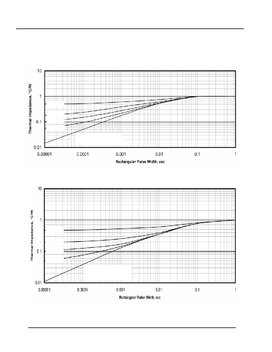
Normalized Thermal Impedance Curves for Both IGBTs and Diodes
SPM6G120-120D
D = 0.50
SINGLE PULSE
(THERMAL RESPONSE)
D = 0.20
D = 0.10
D = 0.05
Figure 5. Normalized Transient Thermal Impedance, Junction-to-Case (Diode)
D = 0.50
D = 0.20
D = 0.10
D = 0.05
SINGLE PULSE
(THERMAL RESPONSE)
Figure 4. Normalized Transient Thermal Impedance, Junction-to-Case (IGBT)

∑
221 West Industry Court Deer Park, NY 11729 (631) 586 7600 FAX (631) 242 9798
∑
∑
World Wide Web Site - http://www.sensitron.com
∑
E-mail Address - sales@sensitron.com
∑
10
SENSITRON
TECHNICAL DATA
Data Sheet 4100 Rev. ≠
Pin Descriptions
LinA ( Pin 1 ), is an isolated drive input for Low-side IGBT of Phase A.
LinA-R ( Pin 2 ), Return for Input at Pin1.
HinA ( Pin 3 ), is an isolated drive input for High-side IGBT of Phase A.
HinA-R ( Pin 4 ), Return for Input at Pin3.
LinB- ( Pin 5 ), is an isolated drive input for Low-side IGBT of Phase B.
LinB-R ( Pin 6 ), Return for Input at Pin5.
HinB ( Pin 7 ), is an isolated drive input for High-side IGBT of Phase B.
HinB-R ( Pin 8 ), Return for Input at Pin7.
LinC ( Pin 9 ), is an isolated drive input for Low-side IGBT of Phase C.
LinC-R ( Pin 10 ), Return for Input at Pin9.
HinC ( Pin 11 ), is an isolated drive input for High-side IGBT of Phase C.
HinC-R ( Pin 12 ), Return for Input at Pin11.
Recommended input turn-on current for all six drive signals is 5-8mA.
For higher noise immunity the tri-state differential buffer, DS34C87, is recommended as shown in Fig. 6.
Note : Connect LinA to non-inverting output for a non-inverting input logic.
Connect LinA to inverting output for an inverting input logic.
Fig. 6. Input Signal Buffer
Opto-
Coupler
Input
LinA
LinA-R
300-400
2-5K
One Channel
of DS34C87
SPM6G120-120D

∑
221 West Industry Court Deer Park, NY 11729 (631) 586 7600 FAX (631) 242 9798
∑
∑
World Wide Web Site - http://www.sensitron.com
∑
E-mail Address - sales@sensitron.com
∑
11
SENSITRON
TECHNICAL DATA
Data Sheet 4100 Rev. -
Flt ( Pin 13 ), is a dual function input/output pin. It is an active low input. It is internally pulled high to +5V by
2.74K
. If pulled down, it will freeze the status of all the six IGBTs regardless of the Hin and Lin signals.
As an output, Pin 13, reports desaturation protection activation. When desaturation protection is activated
a low output for about 9
µ
sec is reported.
If any other protection feature is activated, it will not be reported by Pin 13.
SD ( Pin 14 ), is a dual function input/output pin. It is an active low input. It is internally pulled high to +5V
by 2.74K
. As a low input it shuts down all IGBTs regardless of the Hin and Lin signals.
SD is internally activated due to desaturation protection, or over-current shutdown.
Desaturation shutdown is a latching feature.
SD can be used to shutdown all IGBTs except the brake IGBT by an external command. An open
collector switch shall be used to pull down SD externally.
Also, SD can be used as a fault condition output. Low output at SD indicates a latching fault situation.
Itrip-Ref ( Pin 15 ), is an adjustable voltage divider reference for over-current shutdown. Internal pull-up to
+5V by 20K
, pull down to ground is 8.87K
,
and hysteresis resistance of
15
K
. The internal set point
is 2.43V, corresponding to over-current shutdown of 97A. The re-start delay time is about 70 usec.
Idco ( Pin 16 ), is an absolute value current sense output of DC bus current. The sensor gain is 0.025V/A.
The internal impedance of this output is 1K
, and internal filter capacitance is 1nF. The frequency
response bandwidth of this signal is about 200KHz.
Flt-Clr( Pin 17 ), is a fault clear input. It can be used to reset a latching fault condition, due to desaturation
protection.
Pin 17 an active high input. It is internally pulled down by 2.0K
. A latching fault due to desaturation can be
cleared by pulling this input high to +5V by 200-500
, or to +15V by 3-5K
,
as shown in Fig. 9.
It is recommended to activate fault clear input for more than 300
µ
sec at startup.
+5V Output ( Pin 18 ), is a +5V output. Maximum output current is 30mA.
+15V Rtn ( Pin 19 ), is signal ground, Gnd1. This pin is internally connected to DC Bus return.
No external connection shall be established between Signal Gnd1 and +VDC Rtn.
Gnd1 is isolated from Gnd2.
Note that Pins 13 to 18 are referenced to Gnd1.
Vcc ( Pin 20 ), is the +15V input biasing supply connection for the controller. Under-voltage lockout
keeps all outputs off for Vcc below 10.5V. Vcc pin should be connected to an isolated 15V power supply.
Vcc recommended limits are 14V to 16V , and shall not exceed 18V. The return of Vcc is pin 19.
Recommended power supply capability is about 70mA.
SPM6G120-120D
∑
221 West Industry Court Deer Park, NY 11729 (631) 586 7600 FAX (631) 242 9798
∑
∑
World Wide Web Site - http://www.sensitron.com
∑
E-mail Address - sales@sensitron.com
∑
12
SENSITRON
TECHNICAL DATA
Data Sheet 4100 Rev. -
IAd ( Pin 21 ), is a +2.5V DC offset used for differential output reading of IAo.
IAo ( Pin 22 ), is phase A hall current sensor output. The output can be measured between Pin22 and
Pin 21 differentially. Zero current corresponds to zero output, current entering Phase A pins will produce
positive output voltage at Pin22, and current out of Phase A pins will produce negative output voltage at
Pin22.
Also, the output can be measured as single ended between Pin22 and Pin24. In this case zero current
will correspond to 2.5V output, current entering Phase A pins will produce positive output voltage above
2.5V, and current out of Phase A pins will produce positive output voltage below 2.5V.
The sensitivity of this sensor is 0.015V/A.
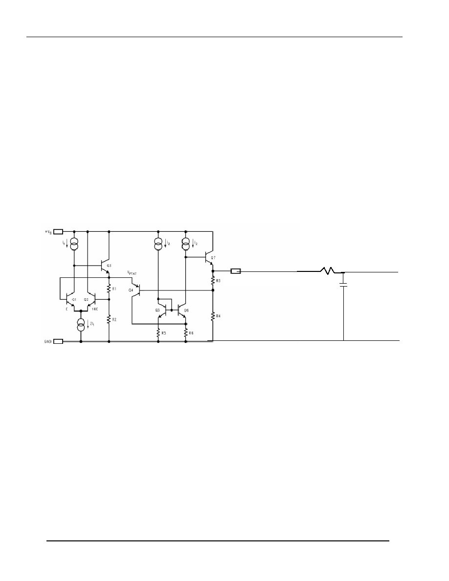
TCo ( Pin 23 ), is an analog output of case temperature sensor. The sensor output gain is 6.25mV/
o
C, with
424 mV DC offset. This sensor can measure both positive and negative
o
C. The internal impedance of this
output is 2.74K
.
The internal block diagram of the temperature sensor is shown in Fig. 7.
The output voltage reading vs temperature will be:
TCo = + 0.58V at Tc= +25
o
C
TCo = + 1.205V at Tc= +125
o
C
TCo = + 0.174V at Tc= -40
o
C
+5V-in Rtn ( Pin 24 ), is signal ground, Gnd2. This pin is internally floating for flexibility. The phase current
sensors and temperature sensor are referenced to Gnd2.
Gnd2 isolation from Gnd1 is over 1500V.
VDD, +5V-in ( Pin 25 ), is the +5V input biasing supply connection for the phase current sensors and
temperature sensor. Pin 25 should be connected to an isolated 5V power supply, recommended limits
are 4.75V to 5.25V. The return of this input is pin 24.
Recommended power supply capability for VDD is about 50mA.
SPM6G120-120D
Fig. 7 Temperature Sensor Internal Block Diagram
Pin 23
2.74K
10nF
Vo= (+6.25mV/
o
C )*T
o
C + 424 mV
Pin 24
Gnd2

∑
221 West Industry Court Deer Park, NY 11729 (631) 586 7600 FAX (631) 242 9798
∑
∑
World Wide Web Site - http://www.sensitron.com
∑
E-mail Address - sales@sensitron.com
∑
13
SENSITRON
TECHNICAL DATA
Data Sheet 4100 Rev. -
ICd ( Pin 26 ), is a +2.5V DC offset used for differential output reading of ICo.
ICo ( Pin 27 ), is hall current sensor output for phase C. The output can be measured between Pin27 and
Pin 26 differentially. Zero current corresponds to zero output, current entering Phase C pins will produce
positive output voltage at Pin27, and current out of Phase C pins will produce negative output voltage at
Pin27.
Also, the output can be measured as single ended between Pin27 and Pin24. In this case zero current
will correspond to 2.5V output, current entering Phase C pins will produce positive output voltage above
2.5V, and current out of Phase C pins will produce positive output voltage below 2.5V.
The sensitivity of this sensor is 0.015V/A.
IBd ( Pin 28 ), is a +2.5V DC offset used for differential output reading of IBo.
IBo ( Pin 29 ), is hall current sensor output for phase B. The output can be measured between Pin29 and
Pin 28 differentially. Zero current corresponds to zero output, current entering Phase B pins will produce
positive output voltage at Pin29, and current out of Phase B pins will produce negative output voltage at
Pin29.
Also, the output can be measured as single ended between Pin29 and Pin24. In this case zero current
will correspond to 2.5V output, current entering Phase B pins will produce positive output voltage above
2.5V, and current out of Phase B pins will produce positive output voltage below 2.5V.
The sensitivity of this sensor is 0.015V/A.
Brk ( Pins 30,31 ), is Brake Terminal. Brake Resistor shall be connected between these terminals and
+VDC. If the brake resistor is inductive, a freewheeling diode shall be connected across this resistor.
Gbrk ( Pin 32 ), is Brake IGBT Gate Input. Brake IGBT Emitter is internally connected to DC Bus return.
+VDC Rtn ( Pins 33 to 37 ), is DC Bus return.
+VDC (Pins 38 to 42 ), is +DC Bus input.
PhC (Pins 43 to 46 ), is Phase C output.
PhB (Pins 47 to 50 ), is Phase B output.
PhA (Pins 51 to 54 ), is Phase A output.
SPM6G120-120D
∑
221 West Industry Court Deer Park, NY 11729 (631) 586 7600 FAX (631) 242 9798
∑
∑
World Wide Web Site - http://www.sensitron.com
∑
E-mail Address - sales@sensitron.com
∑
14
SENSITRON
TECHNICAL DATA
Data Sheet 4100 Rev. -
Pins 55 to 60 are optional. In addition to the internal bootstrap circuits, of Pins 55-60 can be used to
supplement additional, 15V power supplies for the high side gate drivers of phases A,B,C. The internal
bootstrap circuits will stay and be supplemented by the additional power supplies. Contact factory if
these pins are not needed. The part number will be SPM6G120-120-A for an option without Pins 55-60.
Vcc1, Vcc2, Vcc3 recommended limits are 14V to 16V , and shall not exceed 18V.
Fig. 8 shows the connection for Vcc3. A diode Da shall be used to prevent current flow from Vcc to Vcc3
incase of voltage variations between the two supplies. Da also acts as an oring diode and provides
blocking incase of Vcc3 failure. Ra soften the initial charging rate of the gate driver power supply.
Recommended power supply capability for Vcc1, Vcc2, Vcc3 is about 15mA.
Vcc1-Rtn (Pin 55 ), is Phase C high-side gate driver 15V power supply return.
Vcc1 (Pin 56 ), is Phase C high-side gate driver 15V power supply. This should be an isolated power
supply. This is an option to replace the internal Bootstrap circuit.
Vcc2-Rtn (Pin 57 ), is Phase B high-side gate driver 15V power supply return.
Vcc2 (Pin 58 ), is Phase B high-side gate driver 15V power supply. This should be an isolated power
supply. This is an option to replace the internal Bootstrap circuit.
Vcc3-Rtn (Pin 59 ), is Phase A high-side gate driver 15V power supply return.
Vcc3 (Pin 60 ), is Phase A high-side gate driver 15V power supply. This should be an isolated power
supply. This is an option to replace the internal Bootstrap circuit.
SPM6G120-120D
Figure 8. Floating 15V Power Supply Connection for High-Side Gate Drive Of PhA
D1
∑
Gate
Driver
+VDC
PhA
Vcc
+15V
Q1H
Q1L
D2
D3
+VDC Rtn
VBS
Pin59
Pin60
5-10uF
+15V
Rtn
Isolated
15V
supply
+15V Rtn
Sgnl Gnd1
Ra = 10-20
Da
Vcc3

∑
221 West Industry Court Deer Park, NY 11729 (631) 586 7600 FAX (631) 242 9798
∑
∑
World Wide Web Site - http://www.sensitron.com
∑
E-mail Address - sales@sensitron.com
∑
15
SENSITRON
TECHNICAL DATA
Data Sheet 4100 Rev. -
Application Notes
a- System Start Up Sequence:
Activate fault clear input for about 300
µ
sec at startup. The micro-controller enable output is inverted
and fed to the second DS34C87 control input. When the controller is in disable mode, the Flt-clr is
enabled and Phase C low-side IGBT is turned on. This allows for the bootstrap circuit of the high-
side IGBT of Phase C to be charged. At the same time, the high-side bootstrap circuits of Phases A
and B will charge through the motor winding. Once the controller is enabled, PWM signals of all
channels should start.
Fig. 9 shows a recommended startup circuit.
Notes:
1- Gnd1 and Gnd2 are isolated grounds from each other.
2- The +5V power supply used for DS34C87 is an isolated power supply.
3- The +15V power supply used for SPM6G120-120D is an isolated power supply.
Truth Table For DS34C87
Input Control
Input
Non-Inverting Output
Inverting Output
H
H H L
L H L H
X L Z Z
SPM6G120-120D
SPM6G120-120D
OutA-P
OutA-N
OutB-N
OutB-P
OutD-P
OutD-N
OutC-N
OutC-P
Gnd
+5V
A/B Cont
C/D Cont
InC
InD
InB
InA
DS34C87
350
LinC
LinC-R
LinB
LinB-R
HinB-R
HinB
HinA
HinA-R
LinA-R
LinA
350
350
350
350
350
350
350
DS34C87
InA
InB
InD
InC
C/D Cont
A/B Cont
+5V
Gnd
OutC-P
OutC-N
OutD-N
OutD-P
OutB-P
OutB-N
OutA-N
OutA-P
HinC
HinC-R
Micro
Controller
Enable
HinA
LinA
HinB
LinB
HinC
LinC
Flt-Clr
2.74K
SFH6186-4
Fig. 9 Input Interface and Startup Circuit
Gnd2
+5V-in
Gnd1
2.74k
2.74k
2.74k
2.74k
2.74k
2.74k
15V
2.74K

∑
221 West Industry Court Deer Park, NY 11729 (631) 586 7600 FAX (631) 242 9798
∑
∑
World Wide Web Site - http://www.sensitron.com
∑
E-mail Address - sales@sensitron.com
∑
16
SENSITRON
TECHNICAL DATA
Data Sheet 4100 Rev. -
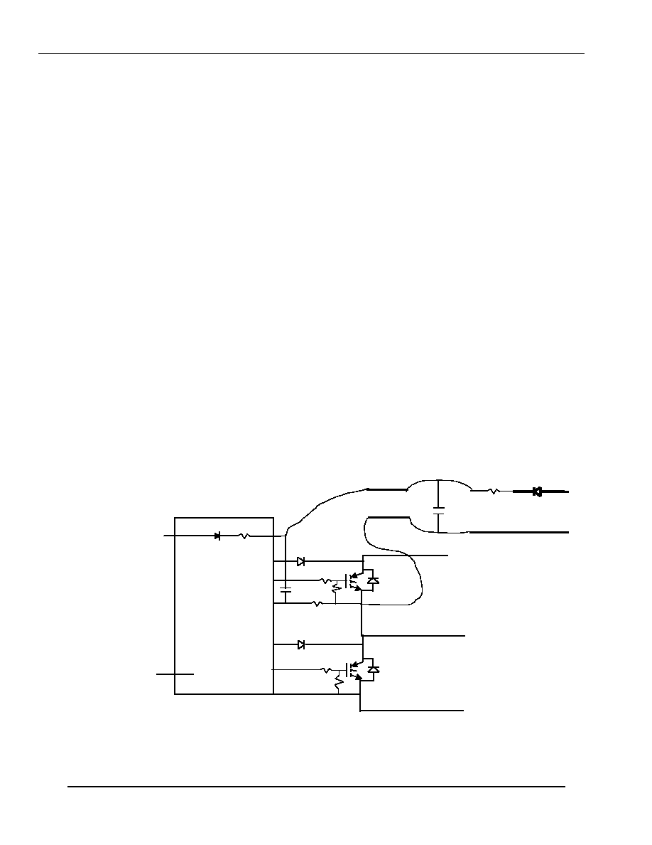
b- DC Bus Charging from 15V
∑
Each IGBT is protected against desaturation.
∑
D2 is the desaturation sense diode for the high-side IGBT
∑
D3 is the desaturation sense diode for the low-side IGBT
∑
When the DC bus voltage is not applied or below 15V, there is a charging path from the
15V supply to the DC bus through D2 and D3 and the corresponding pull up 100K Ohm
resistor. The charging current is 0.15mA per IGBT. Total charging current is about
1.5mA.
∑
Do not apply PWM signal if the DC bus voltage is below 20V.
c- Active Bias For Desaturation Detection Circuit:
The desaturation detection is done by diode D2 for the high side IGBT Q1H, and by diode
D3 for the low side IGBT Q1L. The internal detection circuit, input DSH for the high-side
and input DSL for the low-side, is biased by the local supply voltage VCC for the low side
and VBS for the high side. When the IGBT is on the corresponding detection diode is on.
The current flowing through the diode is determined by the internal pull resistor, R1 for the
high side and R2 for the low side. To minimize the current drain from VCC and VBS, R1
and R2 are set to be 100K
. Lower value of R1 will overload the bootstrap circuit and
reduce the bootstrap capacitor holding time.
SPM6G120-120D
DSH
DSL
D1
∑
Gate
Driver
+15V Rtn
Sgnl Gnd1
+VDC
PhA
Vcc
+15V
Q1H
Q1L
D2
D3
R1
100K
700
K
R2
100K
700
K
+VDC Rtn
Figure 10. Charging Path from 15V Supply to DC Bus when DC Bus is off
VBS

∑
221 West Industry Court Deer Park, NY 11729 (631) 586 7600 FAX (631) 242 9798
∑
∑
World Wide Web Site - http://www.sensitron.com
∑
E-mail Address - sales@sensitron.com
∑
17
SENSITRON
TECHNICAL DATA
Data Sheet 4100 Rev. -
To increase the circuit noise immunity, an active bias circuit is used to lower R1 and R2
when the corresponding IGBT is off by monitoring the input voltage at both DSH, DSL
inputs. If the inputs at DSH drops below 7V the active bias is disabled. The active bias
circuits result in reducing R1 or R2 to about 110
when the corresponding input is above
8V, as shown in Fig. 11. This active circuit results in higher noise immunity.
d- Limitation With Trapezoidal Motor Drive
In trapezoidal motor drives, two phases are conducting while the third phase is off at any
time. In Fig. 12 shows the voltage waveform across one phase, during intervals t1 and t2,
the IGBT is off while the active bias circuit is above 8V, and below 15V. This results in
activating the active pull up circuit and reducing the corresponding R1 or R2 down to about
110
. A high current will flow from VCC or VBS through R2 or R1 and the motor winding
during intervals t1, and t2. This results in draining the bootstrap capacitor voltage quickly.
∑
Contact the factory for adjustments to satisfy trapezoidal motor drive
applications using this module. The adjustment will disable the internal pull up
circuit.
Figure 11. Active Bias for DSH and DSL Internal Inputs
R1
100K
R1
110
7V 8V
VDSH
R1
Figure 12. Active Bias for DSH and DSL Internal Inputs
t1
V
t2
time
15
8
SPM6G120-120D

∑
221 West Industry Court Deer Park, NY 11729 (631) 586 7600 FAX (631) 242 9798
∑
∑
World Wide Web Site - http://www.sensitron.com
∑
E-mail Address - sales@sensitron.com
∑
18
SENSITRON
TECHNICAL DATA
Data Sheet 4100 Rev. -
DISCLAIMER:
1- The information given herein, including the specifications and dimensions, is subject to change without prior notice to improve product
characteristics. Before ordering, purchasers are advised to contact the Sensitron Semiconductor sales department for the latest version of the
datasheet(s).
2- In cases where extremely high reliability is required (such as use in nuclear power control, aerospace and aviation, traffic equipment, medical
equipment , and safety equipment) , safety should be ensured by using semiconductor devices that feature assured safety or by means of users'
fail-safe precautions or other arrangement .
3- In no event shall Sensitron Semiconductor be liable for any damages that may result from an accident or any other cause during operation of
the user's units according to the datasheet(s). Sensitron Semiconductor assumes no responsibility for any intellectual property claims or any
other problems that may result from applications of information, products or circuits described in the datasheets.
4- In no event shall Sensitron Semiconductor be liable for any failure in a semiconductor device or any secondary damage resulting from use at
a value exceeding the absolute maximum rating.
5- No license is granted by the datasheet(s) under any patents or other rights of any third party or Sensitron Semiconductor.
6- The datasheet(s) may not be reproduced or duplicated, in any form, in whole or part, without the expressed written permission of Sensitron
Semiconductor.
7- The products (technologies) described in the datasheet(s) are not to be provided to any party whose purpose in their application will hinder
maintenance of international peace and safety nor are they to be applied to that purpose by their direct purchasers or any third party. When
exporting these products (technologies), the necessary procedures are to be taken in accordance with related laws and regulations.
SPM6G120-120D