Äîêóìåíòàöèÿ è îïèñàíèÿ www.docs.chipfind.ru

·
221 West Industry Court Deer Park, NY 11729 (631) 586 7600 FAX (631) 242 9798
·
·
World Wide Web Site - http://www.sensitron.com
·
E-mail Address - sales@sensitron.com
·
Page 1 of 13
SENSITRON
SEMICONDUCTOR
TECHNICAL DATA
Datasheet 4982, Rev.
Three-Phase MOSFET BRIDGE, With Gate Driver and Optical
Isolation, 600 VOLT, 20 AMP
ELECTRICAL CHARACTERISTICS PER IGBT DEVICE
(Tj=25
0
C UNLESS OTHERWISE SPECIFIED)
P
P
A
A
R
R
A
A
M
M
E
E
T
T
E
E
R
R
S
S
Y
Y
M
M
B
B
O
O
L
L
M
M
I
I
N
N
T
T
Y
Y
P
P
M
M
A
A
X
X
U
U
N
N
I
I
T
T
MOSFET SPECIFICATIONS
Drain to Source Breakdown Voltage
I
C
= 250
µ
A, V
GS
= 0V
BV
CSS
600
-
V
Continuous Drain Current T
C
= 25
O
C
T
C
= 90
O
C
I
D
-
-
20
10
A
Pulsed Drain Current, 1mS
I
DM
40
A
Gate to Source Voltage
V
GS
-
-
+/-20
V
Gate-Source Leakage Current , V
GS
= +/-20V
I
GSS
+/-
100
nA
Gate Threshold Voltage, I
C
=1mA V
GS(TH)
2.0
4.0 V
Zero Gate Voltage Drain Current
V
CS
= 600 V, V
GE
=0V T
i
=25
o
C
V
CS
= 480 V, V
GE
=0V T
i
=125
o
C
I
CSS
-
-
250
500
µ
A
µ
A
On-State Resistance, T
C
= 25
O
C
T
C
= 150
O
C
I
D
= 10A, V
CC
= 15V,
R
DSon
-
0.19
0.43
0.20 V
Input Capacitance
Output Capacitance
Reverse Transfer Cap.
V
CS
= 25 V, V
GE
= 0 V, f = 1 MHz
C
iss
C
oss
C
res
2400
780
50
pF
Over-Temperature Shutdown
Over-Temperature Shutdown
Tsd 100
107
115
o
C
Over-Temperature Output
Tso
10
mV/
o
C
Temperature Sensor Output DC Offset
+0.0
mV
Accuracy, at temperature range from 0
o
C to 125
o
C
+/-1.0
+/-2.0
o
C
Over-Temperature Shutdown Hysteresis
20
o
C
SPM6M020-060D

·
221 West Industry Court Deer Park, NY 11729 (631) 586 7600 FAX (631) 242 9798
·
·
World Wide Web Site - http://www.sensitron.com
·
E-mail Address - sales@sensitron.com
·
Page 2 of 13
SENSITRON
TECHNICAL DATA
Datasheet 4982, Rev.
Gate Driver , - 40
O
C <T
C
< 125
O
C
Supply Voltage
VCC 10
15
20
V
Input On Current
HIN, LIN
2
5.0
mA
Opto-Isolator Logic High Input Threshold
I
th
- 1.6 -
mA
Input Reverse Breakdown Voltage
BV
in
5.0
-
-
V
Input Forward Voltage @ I
in
= 5mA
V
F
-
1.5
1.7
V
Under Voltage Lockout
VCCUV 11.5
-
12.5 V
ITRIP Reference Voltage
(1)
Itrip-ref 1.60
1.65
1.7 V
Input-to-Output Turn On Delay
Output Turn On Rise Time
Input-to-Output Turn Off Delay
Output Turn Off Fall Time
At (VDD=200V, RD=20
, ID=10A), T
j
= 25 to 125
O
C
t
ond
t
r
t
offd
t
f
-
-
-
-
500
20
550
20
700
30
750
30
nsec
Input-Output Isolation Voltage
- 1500
-
-
V
Module
Maximum operating Junction Temperature
T
jmax
-40
-
150
o
C
Maximum Storage Junction Temperature
T
jmax
-55
-
150
o
C
Maximum Thermal Resistance (Junction to Module base
plate) per Mosfet
R
JB
- - 0.80
o
C/W
DC Bus Absolute Maximum Voltage
V+
600
V
DC Bus Recommended Voltage
V+ 100
400
V
DC Bus Absolute Maximum Current, T
C
= 25
O
C
(2)
Idc
20
A
(1)
ITRIP Cycle-by cycle current limit is internally set to 17A peak. The set point can be lowered by connecting a resistor
between Itrip-ref and Gnd. The set point can be increased by connecting a resistor between Itrip-ref and +5V ref
(2)
At elevated case temperature above 25
o
C, the device shall be derated so that the power MOSFETs maximum Junction
temperature is 150
o
C.
SPM6M020-060D

·
221 West Industry Court Deer Park, NY 11729 (631) 586 7600 FAX (631) 242 9798
·
·
World Wide Web Site - http://www.sensitron.com
·
E-mail Address - sales@sensitron.com
·
Page 3 of 13
SENSITRON
TECHNICAL DATA
Datasheet 4982, Rev. -
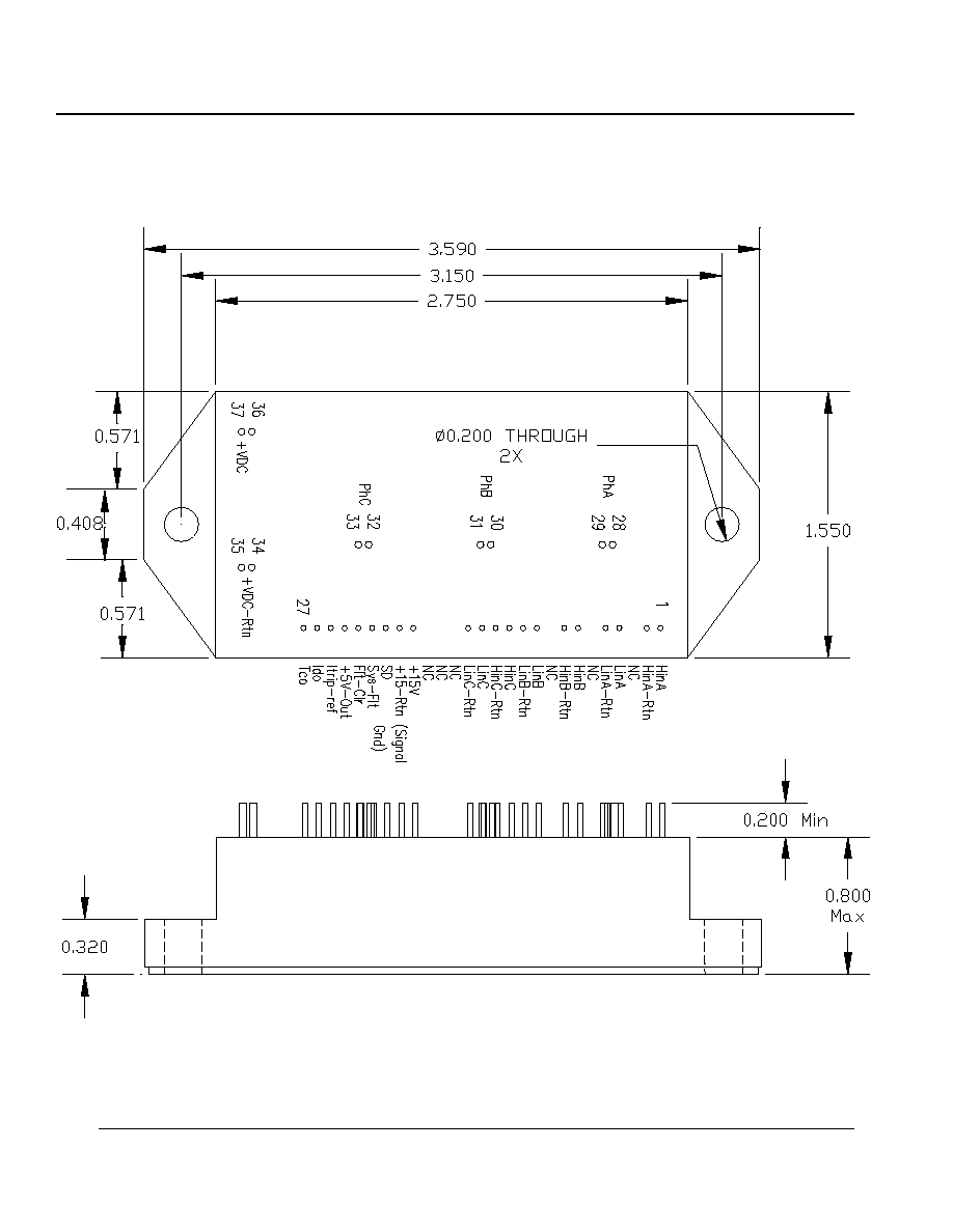
Pin Description
Pin Number
Function
Pin Number
Function
1
Isolated Input for High-side IGBT of
Phase A
18
NC
2
Return for Input at 1
19
+15V Input
3 NC
20
+15V Rtn (Signal Ground)
(2)
4
Isolated Input for Low-side IGBT of
Phase A
21
SD
(2)
5
Return for Input at 4
22
Fault Output
(2)
6 NC
23
Fault Clear Input
(2)
7
Isolated Input for High-side IGBT of
Phase B
24
+5V
Output
8
Return for Input at 7
25
Over-Current Trip Set Point
(2)
9
NC
26
DC Bus Current Output with Total Gain of
0.10 V/A
10
Isolated Input for Low-side IGBT of
Phase B
27
Case Temperature Output with Gain of
0.010 V/
o
C
11
Return for Input at 10
28 &29
Phase A Output
12
Isolated Input for High-side IGBT of
Phase C
30 & 31
Phase B Output
13
Return for Input at 12
32 & 33
Phase C Output
14
Isolated Input for Low-side IGBT of
Phase C
34 & 35
DC Bus "+VDC Return"
15
Return for Input at 14
36 & 37
DC Bus "+VDC" Input
16
NC
Case
Isolated From All Terminals
17 NC
(2) See Pin Description.
SPM6M020-060D
·
221 West Industry Court Deer Park, NY 11729 (631) 586 7600 FAX (631) 242 9798
·
·
World Wide Web Site - http://www.sensitron.com
·
E-mail Address - sales@sensitron.com
·
Page 4 of 13
SENSITRON
TECHNICAL DATA
Datasheet 4982, Rev.
Package Drawing Top View
(All dimensions are in inches, tolerance is +/- 0.010")
SPM6M020-060D
Figure 2. Mechanical Outlines
Base Plate Flatness 0.010" Concave

·
221 West Industry Court Deer Park, NY 11729 (631) 586 7600 FAX (631) 242 9798
·
·
World Wide Web Site - http://www.sensitron.com
·
E-mail Address - sales@sensitron.com
·
Page 5 of 13
SENSITRON
TECHNICAL DATA
Datasheet 4982, Rev. -
Package Pin Locations
(All dimensions are in inches; tolerance is +/- 0.005" except otherwise specified)
Package Material:
Base:
Copper
Frame:
Epoxy
Molded
Case: Epoxy Molded
Power
Terminals:
Copper
SPM6M020-060D
Figure 3. Mechanical Outlines