 | –≠–ª–µ–∫—Ç—Ä–æ–Ω–Ω—ã–π –∫–æ–º–ø–æ–Ω–µ–Ω—Ç: SG6841 | –°–∫–∞—á–∞—Ç—å:  PDF PDF  ZIP ZIP |
Product Specification
Highly-Integrated Green-Mode PWM Controller
SG6841x3
FEATURES
Continuously Decreasing PWM Frequency
Low Start-Up Current (8uA)
Low Operating Current (4mA)
Peak-current-mode Control
Cycle-by-Cycle Current Limiting
Programmable PWM frequency
Leading-Edge Blanking
Synchronized Slope Compensation
Constant Power Limit (Full AC Input Range)
Totem Pole Output with Soft Driving
Programmable Over Temperature Protection (OTP)
Internal Open-loop Protection
V
DD
Under-voltage Lockout (UVLO)
GATE Output Maximum Voltage Clamp (18V)
APPLICATIONS
General-purpose switch-mode power supplies and
flyback power converters, including:
Power Adapters
Open-Frame SMPS
DESCRIPTION
The highly integrated SG6841x3 series of PWM
controllers provides several features to enhance the
performance of flyback converters.
To minimize standby power consumption, a
proprietary green-mode function provides off-time
modulation to continuously decrease the switching
frequency at light-load conditions. This green-mode
function enables the power supply to easily meet
international power conservation requirements. To further
reduce power consumption, SG6841x3 is manufactured
by using the BiCMOS process. This allows the lowest
start-up current around 8uA, and the operating current is
only 4mA. As a result, large start-up resistance can be
used.
SG6841x3's built-in synchronized slope
compensation achieves stable peak-current-mode control.
The proprietary internal line compensation ensures
constant output power limit over a wide AC input voltages,
from 90VAC to 264VAC.
SG6841x3 provides many protection functions. In
addition to cycle-by-cycle current limiting, the internal
open-loop protection circuit ensures safety should an
open-loop or output-short-circuit failure occur. PWM
output is disabled till V
DD
drops below the UVLO lower
limit. Then, the controller starts up again. For OTP, an
external NTC thermistor can be applied for
over-temperature protection.
SG6841x3 is available in an 8-pin DIP or SOP
package.
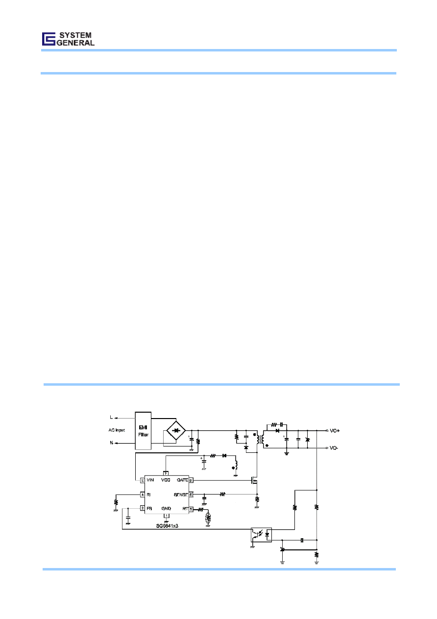
TYPICAL APPLICATION
© System General Corp. - 1 - www.sg.com.tw
Version 1.0(IAO33.0012.B1) Sep. 14, 2005
Product Specification
Highly-Integrated Green-Mode PWM Controller
SG6841x3
© System General Corp. - 2 - www.sg.com.tw
Version 1.0(IAO33.0012.B1) Sep. 14, 2005
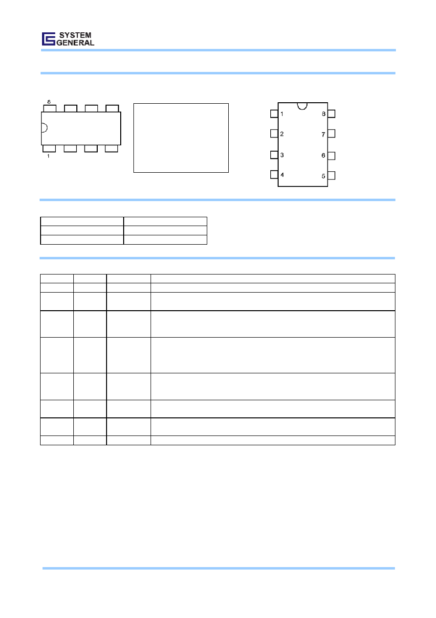
MARKING DIAGRAMS PIN CONFIGURATION
RI
VIN
FB
GND
RT
SENSE
VDD
GATE
T
: D = DIP, S = SOP
P :
Z =Lead Free + ROHS
Compatible
M
: Mask Version
XXXXXX
: Wafer Lot
YY
: Year;
WW
: Week
V
: Assembly Location
SG6841TP
MXXXXXXYYWWV
ORDERING INFORMATION
Part Number
Package
SG6841SZ3
8-Pin SOP (Lead Free)
SG6841DZ3
8-Pin DIP (Lead Free)
PIN DESCRIPTIONS
Pin No. Symbol Function
Description
1 GND
Ground
Ground.
2 FB
Feedback
The signal from the external compensation circuit is fed into this pin. The PWM duty cycle is
determined in response to the signal on this pin and the current-sense signal on Pin 6.
3 VIN
Start-Up
Input
For start-up, this pin is pulled high to the line input via resistors. A large start-up resistance can
be used to minimize power loss. This pin also serves to detect the line voltage for
output-power-limit compensation.
4 RI
Reference
Setting
A resistor connected from the RI pin to ground sets the internal reference current of SG6841x3.
This determines the PWM frequency, open-loop-protection delay time, and RT pin current out.
Increasing the resistance decreases the internal reference current, and thereby reduces the
PWM frequency and delay time.
5 RT
Temperature
Detection
An external NTC thermistor is connected from this pin to ground for over-temperature
protection. The impedance of the NTC decreases at high temperatures. Once the voltage of
the RT pin drops below a fixed limit, PWM output will be disabled.
6 SENSE
Current
Sense
Current sense. The sensed voltage is used for peak-current-mode control and cycle-by-cycle
current limiting.
7 VDD
Power
Supply
Power Supply. The internal protection circuit disables PWM output as long as V
DD
exceeds the
OVP trigger point.
8
GATE
Driver Output
The totem-pole output driver. Soft driving waveform is implemented for improved EMI.

Product Specification
Highly-Integrated Green-Mode PWM Controller
SG6841x3
BLOCK DIAGRAM
Slope
Compensation
1
GND
RT
5
0.65V
+
_
I
RT
VDD
UVLO
7
16V/10V
_
+
Comp
Internal
BIAS
Q
S
R
Comp
Green Mode
Controller
OSC
0.85V
VIN
3
+
_
RI
4
ON/OFF
Driver
FB
2
6V
SENSE
6
GATE
8
VDD
Limited Power
Controller
2R
R
4.2V
© System General Corp. - 3 - www.sg.com.tw
Version 1.0(IAO33.0012.B1) Sep. 14, 2005
Product Specification
Highly-Integrated Green-Mode PWM Controller
SG6841x3
ABSOLUTE MAXIMUM RATINGS
Symbol
Parameter
Test Condition
Value
Unit
V
DD
Supply
Voltage
30
V
V
IN
Input Terminal
30
V
V
L
Input Voltage to FB, SENSE, RT, RI, CS Pin
-0.3 to 7V
mA
P
D
Power
Dissipation
T
A
< 50∞C DIP
SOP
800
400
mW
R
J-A
Thermal
Resistance
Junction-Air DIP
SOP
82.5
141
∞C/W
T
J
Operating Junction Temperature
-40 to +125
∞C
T
STG
Storage Temperature Range
-55 to +150
∞C
T
L
Lead Temperature (Soldering)
10 sec DIP
10 sec SOP
260
230
∞C
ESD Capability, HBM Model
3.0
kV
ESD Capability, Machine Model
250
V
*All voltage values, except differential voltages, are given with respect to GND pin.
* Stresses beyond those listed under "absolute maximum ratings" may cause permanent damage to the device.
RECOMMENDED OPERATING CONDITIONS
Symbol Parameter
Value
Unit
T
A
Operating Ambient Temperature
-20 to +85
R
I
Current source Setting
26 kohms
ELECTRICAL CHARACTERISTICS (VDD = 15V, T
A
= 25∞C, unless noted)
VDD Section
Symbol Parameter
Test
Condition
Min. Typ. Max. Unit
V
OP
Continuously Operating Voltage
24.7
V
V
TH-ON
On Threshold Voltage
15
16
17
V
V
TH-OFF
Off Threshold Voltage
9
10
11
V
I
DD-ST
Start-up
Current
V
DD
= 14.5V
30
uA
I
DD-OP
Operating Supply Current
V
DD
= 15V, RI = 26k, GATE
= open
4 5 mA
T
OVP
V
DD
Over-voltage-protection Debounce
RI = 26k
100
uS
RI Section
Symbol Parameter
Test
Condition
Min. Typ. Max. Unit
RI
NOR
R
I
Operating Range
13
36
k
RI
MAX
Max.
R
I
value for Protection
1
M
RI
MIN
Min. R
I
value for Protection
6
k
Oscillator Section
© System General Corp. - 4 - www.sg.com.tw
Version 1.0(IAO33.0012.B1) Sep. 14, 2005
Symbol Parameter
Test
Condition
Min. Typ. Max. Unit
F
OSC
Normal PWM Frequency
RI = 26k
62 65 68 kHz
F
OSC-G-MIN
Green-Mode Min. Frequency
RI = 26k 4
10
16
kHz
F
DV
Frequency Variation Versus V
DD
Deviation
VDD = 11.5V to 22V
5
%
Product Specification
Highly-Integrated Green-Mode PWM Controller
SG6841x3
F
DT
Frequency Variation Versus Temp. Deviation T
A
= -30
o
C ~ 85
o
C
5
%
Feedback Input Section
Symbol Parameter
Test
Condition
Min. Typ. Max. Unit
A
V
FB Input to Current Comparator Attenuation
1/3.75
1/3.2
1/2.75
V/V
Z
FB
Input
Impedance
4 7 k
V
HiGH
Output High Voltage
FB pin open
5
6
V
V
FB-OL
FB Open-loop Trigger Level
4.2 4.5 4.8 V
T
OLP
FB Open-loop Protection Delay
RI = 26k
26 29 32 mS
V
N
Green-mode Entry FB Voltage
RI = 26k
2.1
V
V
G
Green-mode Ending FB Voltage
V
N
- 0.5
V
V
ZERO
Zero-duty FB Voltage
V
N
- 0.7
V
I
ZERO
Zero-duty FB Current
1.5
mA
Current-Sense Section
Symbol Parameter
Test
Condition
Min. Typ. Max. Unit
Z
CS
Input
Impedance
12
k
V
TH80
Threshold voltage for current limit@80uA
I
VIN
= 80uA, RI = 26k 0.81 0.84 0.87 V
V
TH160
Threshold voltage for current limit@160uA
I
VIN
= 160uA, RI = 26k
V
TH80
-55 V
TH80
-70 V
TH80
-85 mV
T
PD
Propagation Delay to GATE Output
150
200
nS
T
LEB
Leading Edge Blanking Time
200
270
350
nS
V
SLOPE
Slope
Compensation
SENSE = 2k, Duty =
DCY
MAX
0.37
V
GATE Section
Symbol Parameter
Test
Condition
Min. Typ. Max. Unit
DCY
MAX
Maximum Duty Cycle
80
85
90
%
V
OL
Output
Voltage
Low
V
DD
=15V, I
O
= 50mA
1.5
V
V
OH
Output
Voltage
High
V
DD
=12V, I
O
= 50mA
8V
V
T
R
Rising Time
V
DD
=15V, C
L
= 1nF
150
250
350
nS
T
F
Falling
Time
V
DD
=15V, C
L
= 1nF
30
50
90
nS
V
clamp
Gate Output Clamping Voltage
V
DD
= 22V
18
19
V
RT Section
Symbol Parameter
Test
Condition
Min. Typ. Max. Unit
I
RT
Output Current of RT pin
RI = 26k 92
100
108
uA
V
OTP-STOP
Trigger Voltage for Over-temperature
Protection
0.585
0.62
0.655
V
V
OTP-RLS
OTP Release Voltage
V
OTP-STOP
+0.03
V
© System General Corp. - 5 - www.sg.com.tw
Version 1.0(IAO33.0012.B1) Sep. 14, 2005