
55
GH6D407B5A/GH6D407B5B
Hologram Lasers
Notice
In the absence of confirmation by device specification sheets,SHARP takes no responsibility for any defects that may occur in equipment using any SHARP
devices shown in catalogs,data books,etc.Contact SHARP in order to obtain the latest device specification sheets before using any SHARP device.
Internet
Internet address for Electronic Components Group http://www.sharp.co.jp/ecg/
s
Absolute Maximum Ratings
(T
C
=25∞C)
Parameter
Symbol
Rating
Unit
1
Optical power output
P
H
6.3
mW
Reverse voltage
Laser
V
R
2
V
2
Operating temperature
T
opr
-10 to +70
∞
C
2
Storage temperature
T
stg
-40 to +85
∞
C
3
Soldering temperature
T
sold
260
∞
C
1
Output power from hologram laser
2
Case temperature
3
At the position of 1.6mm or more from the lead base (Within 5s)
Monitor photodiode
30
OPIC supply voltage
V
CC
6
V
V
¯8.2
+
≠
+ ≠
0
0.05
3
+
≠
0
0.1
0.8
±
0.2
5=4
±
0.2
2.4
±
0.15
(1.5)
0.4
±
0.1
45∞
±
1∞
45∞
±
1∞
3
0 0.1
Hologram device
Emission point
1.32
±
0.08 from reference plane
Reference plane
Z
X
Y
Z
X
Y
Y
Z
X
¯8.2
+
≠
0
0.05
¯6.1 to 6.3
¯6.6
±
0.2
3.2
±
0.15
4.77
±
0.15
3.8
±
0.5
2.0
±
0.15
(0.8
±
0.2
)
3.3
±
0.2
1.2
±
0.2
12-0.4
±
0.1
2
±
0.2
(0.5
±
0.2
)
¯7.5
MAX.
A B C D E F G H
I
J
RF
y
V
A+F
i
V
B+E
u
V
G+H
r
V
I+J
t
V
S
!0
V
CC
!1
GND
!2
LD
q
Monitor PD (GH6D407B5A)
w
Monitor PD (GH6D407B5B)
w
V
C
o
V
D
e
H
H
H
H
H
H
H
H
+
+
+
shows high-speed amplifier.
) Stem block (metal portion)
is internally connected to GND.
GH6D407B5A/GH6D407B5B
s
Outline Dimensions
3mm Thickness Resin Stem Hologram
Laser for
10 Speed DVD-ROM Drive
qwerty
!2!1!0oiu
Y
X
Z
Terminal connection
Pin configuration
(Unit : mm)
s
Features
(1) With built-in high speed response OPIC
(MIN. 60MHz)
(2) For
10 speed DVD-ROM drives
(3) Thin package (3.0mm thickness) due to insert frame
structure
(4) For reading of low reflective disc (DVD-R, DVD-RAM,
DVD-RW) due to built-in RF amp.
(5) With built-in beam splitter and diffraction grating
OPIC : (Optical IC) is a trademark of the SHARP
Corporation. An OPIC consists of a light-
detecting element and signal-processing circuit
integrated onto a single chip.
s
Model No.
(1)
GH6D407B5A
....Dual power supply
(2)
GH6D407B5B
....Single power supply
s
Applications
(1) DVD-ROM drives
(2) DVD-ROM drives for notebook PC
56
GH6D407B5A/GH6D407B5B
Hologram Lasers
s
Electro-optical Characteristics
(V
CC
=5V, Vs=1/2V
CC
, T
C
=25∞C)
Parameter
Symbol
MAX.
Unit
1
Focal offset
DEF
+0.5
µ
m
Differential efficiency
d
0.84
mW/mA
Conditions
MIN.
TYP.
V
RF
=1.0V
-0.5
-
3.8mW
I(4.75mW)-I(0.95mW)
0.35
0.55
2
Focal error symmetry
B
FES
V
RF
=1.0V
-25
-
+25
%
3
Radial error balance
B
RES
-25
-
+25
%
P
H
=4.75mW
4
RF output amplitude
V
RF
P
H
=4.75mW
0.75
1.05
1.35
V
5
FES output amplitude
V
FES
V
RF
=1.0V
0.51
0.66
0.83
V
75
(100)
125
%
Jitter
V
RF
=1.0V
-
-
12
%
Threshold current
I
th
-
-
27
35
mA
Operating voltage
V
op
P
H
=4.75mW
-
2.2
2.7
V
Wavelength
p
P
H
=4.75mW
640
654
660
nm
Output current
I
m
P
H
=4.75mW, V
R
=15V
0.055
(0.15)
0.26
mA
6
Main spot balance
GH6D407B5A
MSB
P
H
=4.75mW
7
Radial spot balance
RSB
P
H
=4.75mW
75
(100)
125
%
Operating current
I
op
P
H
=4.75mW
-
36
49
mA
1
Distance between FES=0 and jitter minimum point
2
(a≠b) / (a+b)
3
DPD signal
4
Amplitude of V
A
+V
B
+V
C
+V
D
(focal servo ON, radial servo ON)
5
V
A+F
≠V
B+E
(Focal vibration)
6
(V
A+F
+V
B+E
) / (V
C
+V
D
) (focal servo ON, radial servo OFF)
7
V
C
/ V
D
(focal servo ON, radial servo OFF)
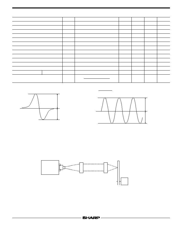
a≠b
2(a+b)
NA=0.60
f =3.3mm
NA=0.13
f =19.07mm
Actuator
Collimated lens
Hologram laser
Single layer DVD disc
Laser driver
APC circuit
Measuring System of Hologram Laser
a (+amplitude of DPD)
b (≠amplitude of DPD)
a (+amplitude of FES)
b (≠amplitude of FES)

57
GH6D407B5A/GH6D407B5B
Hologram Lasers
s
Electrical Characteristics of Monitor Photodiode (Design Standard)
(T
C
=25∞C)
s
Electro-optical Characteristics of Laser Diode (Design Standard)
(T
C
=25∞C)
Parameter
Symbol
MAX.
Unit
Half intensity angle
Deviation
angle
¯
//
+2.1
∞
+3
Misalignment position
x
+80
µ
m
z
+80
µ
m
6
Interference pattern intensity
1
-
Conditions
MIN.
TYP.
Parallel
-2.1
-
Perpendicular
-3
-
∞
-80
-
-80
-
Po=3mW
-
-
¯
y
-80
-
+80
µ
m
-
Parameter
Symbol
MAX.
Unit
1
Sensitivity
S
-
mA/mW
1
Terminal capacitance
C
t
-
pF
Conditions
MIN.
TYP.
-
0.032
Dark current
-
-
nA
-
8.5
I
D
V
R
=15V
s
Electro-optical Characteristics of OPIC for Signal Detection (Design Standard)
(T
C
=25∞C, V
CC
=5V, Vs=2.5V)
Parameter
Symbol
Unit
2
Segment
Supply voltage
V
CC
V
-
Group delay
tgd
ns
V
C
, V
D
, V
RF
Conditions
MIN.
TYP.
4.5
5.0
-
5
-
2
Applicable divisions correspond to output terminals
3
Difference from Vs
4
Difference from GND
5
Output amplitude=0dB (input signal 1MHz)
Load resistance R
L
=10k
, load capacitance C
L
=10pF (For V
RF
,
load capacitance C
L
=10pF)
6
Noise solution against feed-back light (Radio frequency
modulation circuit) is required.
Segment No.
Output
A + F ...........................................V
AF
B + E ...........................................V
BE
C ............................................V
C
D ............................................V
D
G + H ..........................................V
GH
I + J ...........................................V
IJ
G
C
H
E
A
B
F
I
D
J
MAX.
5.5
Supply current
I
CC
-
10
17
24
mA
-
Off-set voltage difference
V
OD1
No light
-25
-
+25
mV
V
AF
-V
BE
, V
C
-V
D
-30
-
+30
mV
V
GH
-V
IJ
f=1 to 36MHz
10
-
-74
-
dBm
V
RF
V
mP
Reference voltage
Vs
-
2.0
2.5
2.63
V
-
34
Output off-set voltage
V
OD1
-30
-
+30
mA
V
AF
, V
BE
, V
C
,
V
D
, V
GH
, V
IJ
1.2
1.36
1.52
V
V
RF
5
Response frequency
f
CF1
-3dB
1
5
-
MHz
V
AF
, V
BE
, V
GH
, V
IJ
f
CF2
60
90
-
MHz
V
C
, V
D
f
CF3
60
90
-
MHz
V
RF
Noise level
f=36MHz, BW=30kHz
Parallel
//
Po=3mW
7
-
11
∞
Perpendicular
25
-
35
∞
V
OD2
Peaking level
V
PK
f=1 to 36MHz
-2
-
+2
dB
V
RF
V
OD2
Emission
characteristics
1
For hologram output power

115
Application Circuits
NOTICE
qThe circuit application examples in this publication are provided to explain representative applications of
SHARP devices and are not intended to guarantee any circuit design or license any intellectual property
rights. SHARP takes no responsibility for any problems related to any intellectual property right of a
third party resulting from the use of SHARP's devices.
qContact SHARP in order to obtain the latest device specification sheets before using any SHARP device.
SHARP reserves the right to make changes in the specifications, characteristics, data, materials,
structure, and other contents described herein at any time without notice in order to improve design or
reliability. Manufacturing locations are also subject to change without notice.
qObserve the following points when using any devices in this publication. SHARP takes no responsibility
for damage caused by improper use of the devices which does not meet the conditions and absolute
maximum ratings to be used specified in the relevant specification sheet nor meet the following
conditions:
(i) The devices in this publication are designed for use in general electronic equipment designs such as:
--- Personal computers
--- Office automation equipment
--- Telecommunication equipment [terminal]
--- Test and measurement equipment
--- Industrial control
--- Audio visual equipment
--- Consumer electronics
(ii)Measures such as fail-safe function and redundant design should be taken to ensure reliability and
safety when SHARP devices are used for or in connection with equipment that requires higher
reliability such as:
--- Transportation control and safety equipment (i.e., aircraft, trains, automobiles, etc.)
--- Traffic signals
--- Gas leakage sensor breakers
--- Alarm equipment
--- Various safety devices, etc.
(iii)SHARP devices shall not be used for or in connection with equipment that requires an extremely
high level of reliability and safety such as:
--- Space applications
--- Telecommunication equipment [trunk lines]
--- Nuclear power control equipment
--- Medical and other life support equipment (e.g., scuba).
qContact a SHARP representative in advance when intending to use SHARP devices for any "specific"
applications other than those recommended by SHARP or when it is unclear which category mentioned
above controls the intended use.
qIf the SHARP devices listed in this publication fall within the scope of strategic products described in the
Foreign Exchange and Foreign Trade Control Law of Japan, it is necessary to obtain approval to export
such SHARP devices.
qThis publication is the proprietary product of SHARP and is copyrighted, with all rights reserved. Under
the copyright laws, no part of this publication may be reproduced or transmitted in any form or by any
means, electronic or mechanical, for any purpose, in whole or in part, without the express written
permission of SHARP. Express written permission is also required before any use of this publication
may be made by a third party.
qContact and consult with a SHARP representative if there are any questions about the contents of this
publication.