 | –≠–ª–µ–∫—Ç—Ä–æ–Ω–Ω—ã–π –∫–æ–º–ø–æ–Ω–µ–Ω—Ç: GL8T156 | –°–∫–∞—á–∞—Ç—å:  PDF PDF  ZIP ZIP |
(Notice)
°
In the absence of confirmation by device specification sheets, SHARP takes no responsibility for any defects that may occur in equipment using any SHARP
devices shown in catalogs, data books, etc. Contact SHARP in order to obtain the latest device specification sheets before using any SHARP device.
(Internet)
°
Data for sharp's optoelectronic/power device is provided for internet.(Address http://www.sharp.co.jp/ecg/)
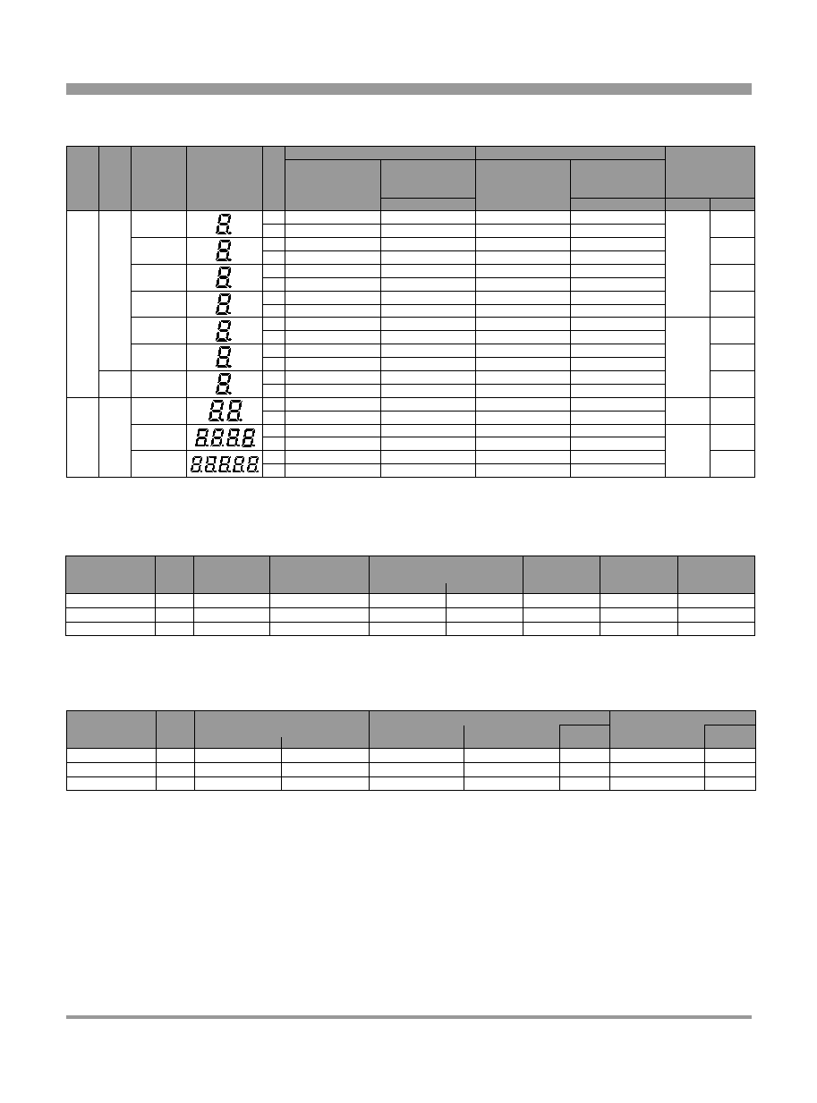
Super-luminosity/High-luminosity Numeric LED
140
Digit
1
-
d
i
g
i
t
M
o
l
d
T
y
p
e
Substrate
Type
M
u
l
t
i
-
d
i
g
i
t
s
M
o
l
d
T
y
p
e
Type
Type of display
Outline dimensions
Model No.
Luminous intensity
(mcd)
TYP.
Model No.
Luminous intensity
(mcd)
TYP.
Page
Figure
*
1
C
o
m
m
o
n
p
i
n
s
Character
height
(mm)
U (Red)
T (Red)
8.0
10.16
14.12
20.32
25.4
38.1
76.0
10.16
8.0
7.6
10
9
8
6
4
3
1
12
19
21
A
K
A
K
A
K
A
K
A
K
A
K
A
K
A
K
A
K
A
K
GL9U100
GL8U100
GL9U15
GL8U15
GL9U30
GL8U30
35.0
35.0
27.0
27.0
(120)*
(120)*
GL9T030
GL8T030
GL9T040
GL8T040
GL9T156
GL8T156
GL9T08
GL8T08
GL9T100
GL8T100
GL7T201
GL6T201
GL3T422
GL3T421
GL3T508D
GL3T507D
4.0
4.0
4.25
4.25
5.25
5.25
2.2
2.2
9.5
9.5
4.25
4.25
1.5
1.5
1.5
1.5
*1 A: Anode common K: Cathode common * Production after order confirmation
* As for current conditions, refer to I
F
in electro-optical characteristics
(Ta=25∞C)
s
Super-luminosity/High-luminosity Numeric LED
Figures shown below are values per segment.
Character height
(mm)
Forward current
I
F
(mA)
Peak forward current
I
FM
*1
(mA)
Derating factor
(mA/ ∞C)
Reverse voltage
V
R
(V)
Operating temperature
T
opr.
(∞C)
Storage temperature
T
stg.
(∞C)
Radiation
color
*1 Duty ratio=1/10, Pulse width=0.1ms
*2 U type duty ratio=1/16, pulse width=0.1ms
8.0/10.16/14.12/20.32
25.4, 38.1, 76.0
25.4, 38.1
T
U
T
20
20
20
100
150
*2
100
0.36
0.36
0.36
5
6
5
-30 to +70
-30 to +70
-30 to +70
-40 to +80
-40 to +80
-40 to +80
1.82
2.73
1.82
DC
Pulse
(Ta=25∞C)
s
Absolute Maximum Ratings
Figures shown below are values per segment.
Character height
(mm)
Forward current
V
F
Peak emission wavelength
p(nm)
TYP.
Radiation
color
8.0/10.16/14.12/20.32
25.4, 38.1, 76.0
25.4, 38.1
T
U
T
1.7
3.5
3.4
2.2
4.8
4.4
660
660
660
Spectrum radiation bandwidth
(
nm)
TYP.
I
F
(mA)
20
20
20
10
10
10
Reverse current
I
R(
µ
A)
MAX.
V
R
(V)
10
100
10
4
5
4
TYP.
MAX
(Ta=25∞C)
s
Electro-optical Characteristics
Figures shown below are values per segment.
(Notice)
°
In the absence of confirmation by device specification sheets, SHARP takes no responsibility for any defects that may occur in equipment using any SHARP
devices shown in catalogs, data books, etc. Contact SHARP in order to obtain the latest device specification sheets before using any SHARP device.
(Internet)
°
Data for sharp's optoelectronic/power device is provided for internet.(Address http://www.sharp.co.jp/ecg/)
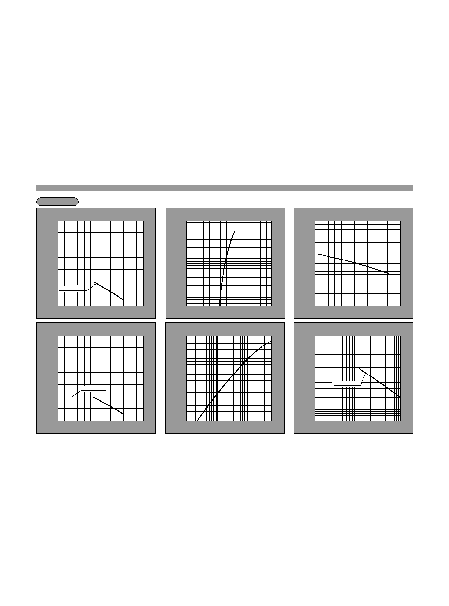
Numeric LED
Characteristics Diagrams
145
T series
D series
* In case of 25.4mm: value per 1segment 1chip
* In case of 25.4/45.0mm: value per 1segment 1chip
(Duty ratio1/10)
0
10
20
30
40
50
60
70
-20
0
20
40
60
100
80
1.1
1.3
1.5
1.7
1.9
2.1
2.3
2.5
0.5
2
1
3
5
10
20
50
100
1.0
1.2
1.4
1.6
1.8
2.0
2.2
2.4
(T
a=
25
∞C)
1
2
5
200
100
20
50
10
500
0.1
0.2
0.5
1
2
5
10
20
50
(T
a=
25
∞C)
(1
F
=20mA/seg)
10
20
50
200
100
500
1000
-20
0
20
40
60
100
80
5
10
30
50
100
300
500
1/50
1/20
1/10
1/5
1/2
1
(T
a=
25
∞C)
0
10
20
30
40
50
60
70
-20
0
20
40
60
100
80
0
10
20
30
40
50
60
70
-20
0
20
40
60
100
80
0
50
100
150
200
250
300
350
-20
0
20
40
60
100
80
(Duty ratio1/10)
0.5
2
1
3
5
10
20
50
100
1.0
1.2
1.4
1.6
1.8
2.0
2.2
2.4
(T
a=
25
∞C)
1.1
1.3
1.5
1.7
1.9
2.1
2.3
2.5
1
2
5
200
100
20
50
10
500
0.1
0.2
0.5
1
2
5
10
20
50
(T
a=
25
∞C)
(1
F
=20mA/seg)
10
20
50
200
100
500
1000
-20
0
20
40
60
100
80
5
10
30
50
100
300
500
1/50
1/20
1/10
1/5
1/2
1
(T
a=
25
∞C)
45.0mm
Substrate type
45.0mm
Substrate type
Forward Current Derating Curve
Forward Current vs. Forward Voltage*
Luminous Intensity vs. Ambient Temperature
Ambient temperature T
a(
∞C)
Forward voltage V
F
(V/seg)
Ambient temperature T
a(
∞C)
F
o
r
w
a
r
d
c
u
r
r
e
n
t
I
F
(
m
A
/
s
e
g
)
F
o
r
w
a
r
d
c
u
r
r
e
n
t
I
F
(
m
A
/
s
e
g
)
R
e
l
a
t
i
v
e
l
u
m
i
n
o
u
s
i
n
t
e
n
s
i
t
y
(
%
)
Mold type
Peak Forward Current Derating Curve
Luminous Intensity vs. Forward Current
Duty Ratio vs. Peak Forward Current
Ambient temperature T
a(
∞C)
Forward current I
F
(mA/seg)
Duty ratio D
R
P
e
a
k
f
o
r
w
a
r
d
c
u
r
r
e
n
t
I
F
M
(
m
A
/
s
e
g
)
R
e
l
a
t
i
v
e
l
u
m
i
n
o
u
s
i
n
t
e
n
s
i
t
y
(
%
)
P
e
a
k
f
o
r
w
a
r
d
c
u
r
r
e
n
t
I
F
(
m
A
/
s
e
g
)
Mold type
Mold type
Forward Current Derating Curve
Forward Current vs. Forward Voltage*
Luminous Intensity vs. Ambient Temperature
Ambient temperature T
a(
∞C)
Forward voltage V
F
(V/seg)
Ambient temperature T
a(
∞C)
F
o
r
w
a
r
d
c
u
r
r
e
n
t
I
F
(
m
A
/
s
e
g
)
F
o
r
w
a
r
d
c
u
r
r
e
n
t
I
F
(
m
A
/
s
e
g
)
R
e
l
a
t
i
v
e
l
u
m
i
n
o
u
s
i
n
t
e
n
s
i
t
y
(
%
)
Mold type
Substrate type
Peak Forward Current Derating Curve
Luminous Intensity vs. Forward Current
Duty Ratio vs. Peak Forward Current
Ambient temperature T
a(
∞C)
Forward current I
F
(mA/seg)
Duty ratio D
R
P
e
a
k
f
o
r
w
a
r
d
c
u
r
r
e
n
t
I
F
M
(
m
A
/
s
e
g
)
R
e
l
a
t
i
v
e
l
u
m
i
n
o
u
s
i
n
t
e
n
s
i
t
y
(
%
)
P
e
a
k
f
o
r
w
a
r
d
c
u
r
r
e
n
t
I
F
(
m
A
/
s
e
g
)
Mold type
Substrate type
Mold type
Substrate type

Numeric LED
Characteristics Diagrams
144
(Notice)
°
In the absence of confirmation by device specification sheets, SHARP takes no responsibility for any defects that may occur in equipment using any SHARP
devices shown in catalogs, data books, etc. Contact SHARP in order to obtain the latest device specification sheets before using any SHARP device.
(Internet)
°
Data for sharp's optoelectronic/power device is provided for internet.(Address http://www.sharp.co.jp/ecg/)
* In case of 25.4/38.1/76.0mm: value per 1segment 1chip
P series
U series
Mold type
Substrate type
0
5
10
15
20
25
30
35
-20
0
20
40
60
100
80
Substrate type
Mold type
0
10
20
30
40
50
60
70
-20
0
20
40
60
100
80
(Duty ratio1/10)
0.5
2
1
3
5
10
20
50
100
1.0
1.2
1.4
1.6
1.8
2.0
2.2
2.4
(T
a=
25
∞C)
1.1
1.3
1.5
1.7
1.9
2.1
2.3
2.5
1
2
5
200
100
20
50
10
500
0.1
0.2
0.5
1
2
5
10
20
50
(T
a=
25
∞C)
(1
F
=5mA/seg)
10
20
50
200
100
500
1000
-20
0
20
40
60
100
80
5
10
30
50
100
300
500
1/50
1/20
1/10
1/5
1/2
1
(T
a=
25
∞C)
0
5
10
15
20
25
30
35
-20
0
20
40
60
100
80
0
50
100
150
-20
0
20
40
60
100
80
(Duty ratio1/10)
1
2
5
200
100
20
50
10
500
0.1
0.2
0.5
1
2
5
10
20
50
(T
a=
25
∞C)
(1
F=
20mA)
10
20
50
200
100
500
1000
-20
0
20
40
60
100
80
150
5
10
30
50
100
300
500
1/50
1/20
1/10
1/5
1/2
1
(T
a=
25
∞C)
0.5
2
1
3
5
10
20
50
100
2.0
2.4
2.8
3.2
3.6
4.0
4.4
4.8
(T
a=
25
∞C)
2.2
2.6
3.0
3.4
3.8
4.2
4.6
5.0
Forward Current Derating Curve
Forward Current vs. Forward Voltage*
Luminous Intensity vs. Ambient Temperature
Ambient temperature T
a
(
∞C)
Forward voltage V
F
(V/seg)
Ambient temperature T
a
(
∞C)
Forward current I
F
(mA/seg)
Forward current I
F
(mA/seg)
Relative luminous intensity(%)
Peak Forward Current Derating Curve
Luminous Intensity vs. Forward Current
Duty Ratio vs. Peak Forward Current
Peak forward current I
FM
(mA/seg)
Relative luminous intensity(%)
Peak forward current I
F
(mA/seg)
Ambient temperature T
a
(
∞C)
Forward current I
F
(mA/seg)
Duty ratio D
R
Mold type
Substrate type
Forward Current Derating Curve
Forward Current vs. Forward Voltage*
Luminous Intensity vs. Ambient Temperature
Ambient temperature T
a
(
∞C)
Forward voltage V
F
(V/seg)
Ambient temperature T
a
(
∞C)
Forward current I
F
(mA/seg)
Forward current I
F
(mA/seg)
Relative luminous intensity(%)
Peak Forward Current Derating Curve
Luminous Intensity vs. Forward Current
Duty Ratio vs. Peak Forward Current
Ambient temperature T
a
(
∞C)
Forward current I
F
(mA/seg)
Duty ratio D
R
Peak forward current I
FM
(mA/seg)
Relative luminous intensity(%)
Peak forward current I
F
(mA/seg)
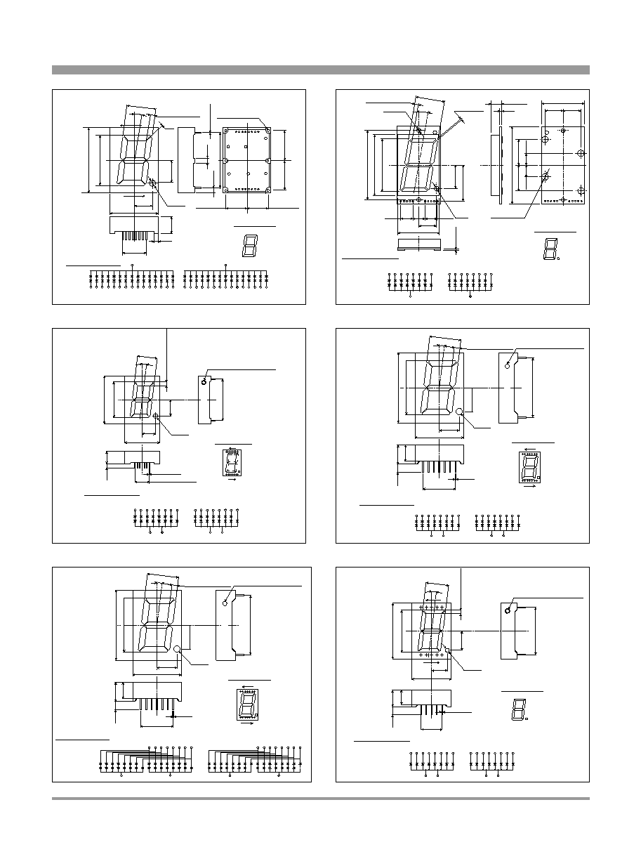
Numeric LED
Outline Dimensions(Unit:mm)
148
(Notice)
°
In the absence of confirmation by device specification sheets, SHARP takes no responsibility for any defects that may occur in equipment using any SHARP
devices shown in catalogs, data books, etc. Contact SHARP in order to obtain the latest device specification sheets before using any SHARP device.
(Internet)
°
Data for sharp's optoelectronic/power device is provided for internet.(Address http://www.sharp.co.jp/ecg/)
D1
3
D2
4
E1
1
E2
2
F1
13
F2
14
G1
15
G2
16
C2
7
D.P.
8
10
B2
9
B1
6
C1
6-¯3.0
±
0.15
Internal connection diagram
12
A2
11
A1
D1
3
D2
4
E1
1
E2
2
F1
13
F2
14
G1
15
G2
16
C2
7
D.P.
8
10
B2
9
B1
6
C1
12
A2
11
A1
98.0
±
0.5
5.08
!
7mm
35.5
!
76.0
±
0.4
33.0
±
0.5
33.0
±
0.5
42.0
±
0.3
10∞
16
9
1
5
5
8
8.0(Segment width)
1.3
+1.3
-0.15
0.8
76.0
±
0.4
45.0
±
0.5
45.0
±
0.5
34.0
25.0
7.5
86.0
!
7.0
7.5
D.P.
¯9.6
A
B
F
E
C
D
G
28.0
Segment name
15.0
15.0
36.0
10.0
1.6
9.0
66.0
22.0
F
E
G
10
3
2
4
8 5
GL8
t
18
¯4.0
4-¯5.5MAX.
(Calking)
(Calking)
C D
D.P.
59.0
24.0
45.0
2-¯3.3
3.0
(Segment width)
10∞
52.0
E F G D.P.
10.16
10.16
10
1
14.5
0.5MA
!
.
8
7
5
4
3
2
10
7
6
6
GL9
t
18
10.16
35.0
(2.54
!
4)
Internal connection diagram
B
A
A B C D
9
9
22.0
10.0
30.5
20.0
1.0 for all space
Segment name
A
B
C
D
E
F
G
D.P.
44.0
∞
7
21.0
17.0
14.0
37.0
51.0
3.9
(Segment width)
38.1
15.24
10-¯0.55
13.0
4.5
¯4.8
Segment name
B
C
E
F
A
G
D
D.P.
Luminous intensity rank
Internal connection diagram
8
14
1
7
2.54
!
6=
S GL8U15
F
E
G
6
12
1
14
5 2
GL8
t
15
C D
D.P.
E F G D.P.
5
8
2
14
12
1
6
8
9
9
GL9
t
15
B
A
A B C D
11
4
11
4
Luminous intensity rank
11.2
27.9
14.7
∞
7
9.4
33.0
25.4
15.24
7.5
4.0
9.0
¯0.55
22.8
¯3.0
2.7(for all segment width)
2.54
!
6=
MIN.
A
G
C
D
D.P.
E
F
B
8
14
7
1
S GL9E100
Internal connection diagram
F
E
G
6
12
1
14
5 2
GL8
t
100
C D
D.P.
E F G D.P.
5
8
2
14
12
1
6
8
9
9
GL9
t
100
B
A
A B C D
11
4
4
11
Segment name
Luminous intensity rank
11.2
27.9
14.7
∞
7
9.4
33.0
25.4
15.24
7.5
4.0
9.0
¯0.55
22.8
¯3.0
2.7(for all segment width)
2.54
!
6=
MIN.
A
G
C
D
D.P.
E
F
B
8
14
7
1
S GL9E100
Internal connection diagram
B
D
F G
C
5
2
E
1 12 14
A
9
8
GL9
tt
100
(Red)
(Yellow-green)
11
4
D.P.
6
B
D
F G
C
5
2
E
1 12 14
A
9
8
GL8
tt
100
(Red)
(Yellow-green)
11
4
D.P.
6
Segment name
9.26
22.86
∞
7
7.6
20.32
27.0
11.0
=10.16
4.0
8.0
7.0
10-¯0.45
1.
8
(Segment width)
19.0
A
B
C
D
E
F
G
D.P.
5
1
10
MIN.
Luminous intensity rank
¯2.0
6
2.54
!
4
S GL8
t
08
Internal connection diagram
F
E
G
5
9
1
10
4 2
GL8
t
08
C D
D.P.
E F G D.P.
4
6
2
10
9
1
5
6
7
7
GL9
t
08
B
A
A B C D
8
3
3
8
Segment name
1
3
5
2
4
6
GL9
t
30 Series GL8
t
30 Series
GL9
t
18 Series GL8
t
18 Series
GL9
t
15 Series GL8
t
15 Series
GL9
t
100 Series GL8
t
100 Series
GL9
tt
100 Series GL8
tt
100 Series
GL9
t
08 Series GL8
t
08 Series
(Notice)
°
In the absence of confirmation by device specification sheets, SHARP takes no responsibility for any defects that may occur in equipment using any SHARP
devices shown in catalogs, data books, etc. Contact SHARP in order to obtain the latest device specification sheets before using any SHARP device.
(Internet)
°
Data for sharp's optoelectronic/power device is provided for internet.(Address http://www.sharp.co.jp/ecg/)
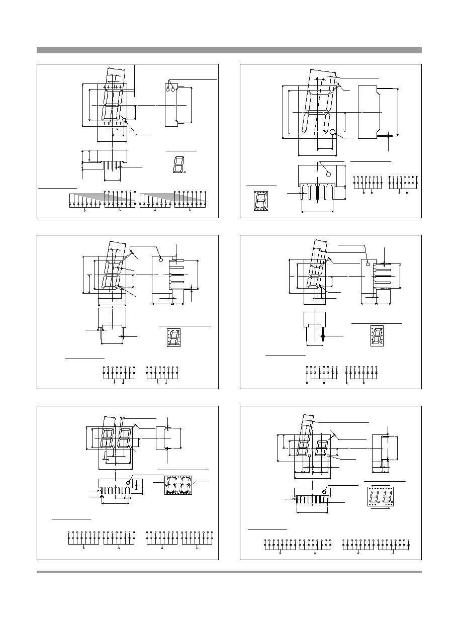
Numeric LED
Outline Dimensions(Unit:mm)
149
Internal connection diagram
Segment name
9
.
2
6
2
2
.
8
6
∞
7
7.6
2
0
.
3
2
2
7
.
0
11.0
=10.16
4
.
0
8
.
0
7
.
0
10-¯0.45
1
.
8
(
S
e
g
m
e
n
t
w
i
d
t
h
)
19.0
A
B
C
D
E
F
G
D.P.
5
1
10
M
I
N
.
Luminous intensity rank
¯2.0
6
2.54
!
4
S
G
L
9
E
D
0
8
G
R
4 2 1 9 10
7 6
GL9
tt
08
(Yellow-green)
3
(Red)
8
(Yellow-green)
3
(Red)
8
B
D
F G
C
E
A
D.P.
5
4 2 1 9 10
7 6
GL8
tt
08
B
D
F G
C
E
A
D.P.
5
1
5
.
2
4
∞
8
¯1.7
6
.
4
1
8.12
4
.
0
7
.
0
Luminous intensity rank
2.54
!
4=10.16
0
.
2
5
12.2
4.85
1
7
.
0
1
4
.
1
2
0.5
5
4
3
2
1
109
6
7
8
D
E
F
G
A
B
C
D.P.
1.3(for all segment width)
(for all space)
0.3
9P156
Internal connection diagram
Segment name
F
E
G
5
9
1
10
4 2
GL8
t
156
C D
D.P.
E F G D.P.
4
6
2
10
9
1
5
6
7
7
GL9
t
156
B
A
A B C D
8
3
3
8
4.0
0
.
5
7.0
1.0
2
.
5
4
!
4
=
1
0
.
1
6
1
.
3
5
∞
0
1
1.0
¯1.2
4.8
9.6
3.2
1
0
.
1
6
6
.
5
4
.
5
8
1
3
.
0
5.6
0.3
Luminous intensity rank
1.35
7.62
0.25
(for all space)
(for all segment width)
D.P.
B
A
F
G
E
C
D
1
2
3
4
5
6
7
8
9
10
G
L
9
S
0
4
0
Internal connection diagram
Segment name & Pin No.
F
E
G
7
2
4
3
8 5
GL8
t
040
C D
D.P.
E F G D.P.
8
9
5
3
2
4
7
9
10
10
GL9
t
040
B
A
A B C D
6
1
1
6
Luminous intensity rank
4.5
5.0
1.0
0
.
5
∞
0
1
4.0
Internal connection diagram
3
.
5
7.0
±
0.3
8
.
0
1
1
.
0
±
0
.
4
5.3
¯0.9
2.2
0.25
2
.
0
!
4
=
8
.
0
-
0
+
0
.
1
5
-0
+0.15
D.P.
1
2
3
4
5
9
8
7
6
10
A
D
E
C
B
F
G
G
L
9
T
0
3
0
1.0(for all segment width)
0.3(for all space)
Segment name & Pin No.
E F G
D.P.
8
10
5
3
2
4
1
6
GL9
t
030
A B C D
7
9
E F G
D.P.
8
10
5
3
2
4
1
7
GL8
t
030
A B C D
6
9
1
.
7
5
0
.
2
5
Dig.2
1
5
.
2
4
8.12
2-¯1.7
1
.
0
Luminous intensity rank
7
.
0
6.35
∞
8
6.35
1.5
25.0
11.2
6
.
4
1
Dig.1
20.32
2.54
4
.
0
1
7
.
0
0.5
1.25
1
4
.
1
2
0.3(Space)
1.3(Segment width)
Internal connection diagram
Segment name & Pin No.
2.54
!
8=
D
1
F
1
E
1
G
1
A
1
B
1
C
1
E
2
F
2
B
2
A
2
G
2
D
2
C
2
18
10
9
1
S GL7D220
D
1
E
1
F
1
G
1
.
15
16
3
18
1
2
17
4
GL7
t
220
D.P
1
A
1
B
1
C
1
14
Dig.1
D
2
E
2
F
2
G
2
10
11
8
12
5
6
7
9
D.P
2
A
2
B
2
C
2
13
Dig.2
D
1
E
1
F
1
G
1
.
15
16
3
18
1
2
17
4
GL6
t
220
D.P
1
A
1
B
1
C
1
14
Dig.1
D
2
E
2
F
2
G
2
10
11
8
12
5
6
7
9
D.P
2
A
2
B
2
C
2
13
Dig.2
0
.
2
5
1.0
4.0
7.0
5
.
0
8
2-¯1.6
1
.
0
1
5
.
2
4
∞
0
1
6.6
1.9
4.3
5.8
6.2
0.9
1
0
.
1
6
1
8
.
0
±
0
.
3
9
.
0
1.5
4.3
24.0
±
0.4
0.5
2.54
!
8=20.32
Internal connection diagram
-0
+0.15
-
0
+
0
.
1
5
1.0(for all segment width)
0.3(for all space)
Luminous intensity rank
Segment name & Pin No.
F
1
E
1
D
1
B
1
B
2
F
2
G
1
D
2
C
1
G
2
A
1
A
2
Dig 1
Dig 2
D.P.2
D.P.1
E
2
C
2
9
1
10
18
S GL7T201
D
1
E
1
F
1
G
1
3
15
2
17
18
1
GL7
t
201
16
A
1
B
1
C
1
14
D
2
E
2
F
2
G
2
10
11
8
12
5
6
7
4
D.P
1
9
D.P
2
A
2
B
2
C
2
13
D
1
E
1
F
1
G
1
15
16
3
18
1
2
17
GL6
t
201
A
1
B
1
C
1
14
D
2
E
2
F
2
G
2
10
11
8
12
5
6
7
4
D.P
1
9
D.P
2
A
2
B
2
C
2
13
7
9
11
8
10
12
GL9
tt
08 Series GL8
tt
08 Series
GL9
t
156 Series GL8
t
156 Series
GL9
t
040 Series GL8
t
040 Series
GL9
t
030 Series GL8
t
030 Series
GL7
t
220 Series GL6
t
220 Series
GL7
t
201 Series GL6
t
201 Series