 | –≠–ª–µ–∫—Ç—Ä–æ–Ω–Ω—ã–π –∫–æ–º–ø–æ–Ω–µ–Ω—Ç: GP1A52 | –°–∫–∞—á–∞—Ç—å:  PDF PDF  ZIP ZIP |
GP1A50HR/GP1A51HR/GP1A52HR/GP1A53HR
GP1A50HR/GP1A51HR
GP1A52HR/GP1A53HR
OPIC
Photointerrupter
s
Features
1. High sensing accuracy ( Slit width : 0.5mm )
2. LSTTL and TTL compatible output
s
Applications
1. OA equipment, such as printers, facsimiles,
2. VCRs
etc.
s
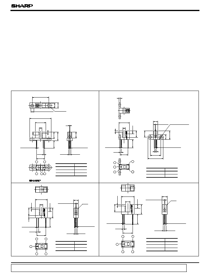
Outline Dimensions
(Unit : mm )
0.5
(9.2)
(1.27)
2
-
C2.0
6.0
5.0
1.5
7.5
10.0
7.0
3.5
GP1A50HR
GP1A52HR
GP1A53HR
A53
S
A52
S
GP1A51HR
1.5
3.5
(9.2)
(1.27)
0.5
Slit width
10.0
5.0
C1.0
7.5
2.5
C1.0
0.5
5.2
(1.27)
10.0
7.5
1.5
(10.3)
1A51HR
1A50HR
3.5
1.5
7.5
(9.2)
Slit width
0.5
2
-
(1.27)
5.0
7.0
12.0
18.0
6.0
10.0
2.0
(1.27)
(1.5)
(1.5)
(1.27)
(1.5)
3.5
(1.5)
(1.27)
1
4 5
3
2
Marking
:
Slit width
(Both sides of
emitter and
detector )
*
Unspecified tolerances shall be as follows
:
Dimensions(d) Tolerance
d
<=
6.0
±
0.1
6.0
<
d
<=
18.0
±
0.2
18.0
<
d
<=
25.0
±
0.025
*
( )
:
Reference dimensions
5
4
3
1
2
(Both sides of
emitter and
detector )
Dimensions(d) Tolerance
d
<=
6.0
±
0.1
6.0
<
d
<=
18.0
±
0.2
*
Unspecified tolerances shall be as follows
:
*
( )
:
Reference dimensions
1A52HR
2
3
1
5
4
(Both sides
of emitter
and detector )
*
Unspecified tolerances shall be as follows
:
*
( )
:
Reference dimensions
Dimensions(d) Tolerance
d
<=
6.0
±
0.1
6.0
<
d
<=
18.0
±
0.2
Slit width
(Both sides
of emitter
and detector )
1A53HR
1
5
4
3
2
*
Unspecified tolerances shall be as follows
:
Dimensions(d) Tolerance
d
<=
6.0
±
0.1
6.0
<
d
<=
18.0
±
0.2
18.0
<
d
<=
25.0
±
0.25
*
( )
:
Reference dimensions
Both-sides mounting type :
GP1A50HR
(Gap: 3mm )
Either-side mounting type :
GP1A51HR
(Gap: 3mm )
PWB mounting type :
GP1A52HR
( Gap: 3mm )
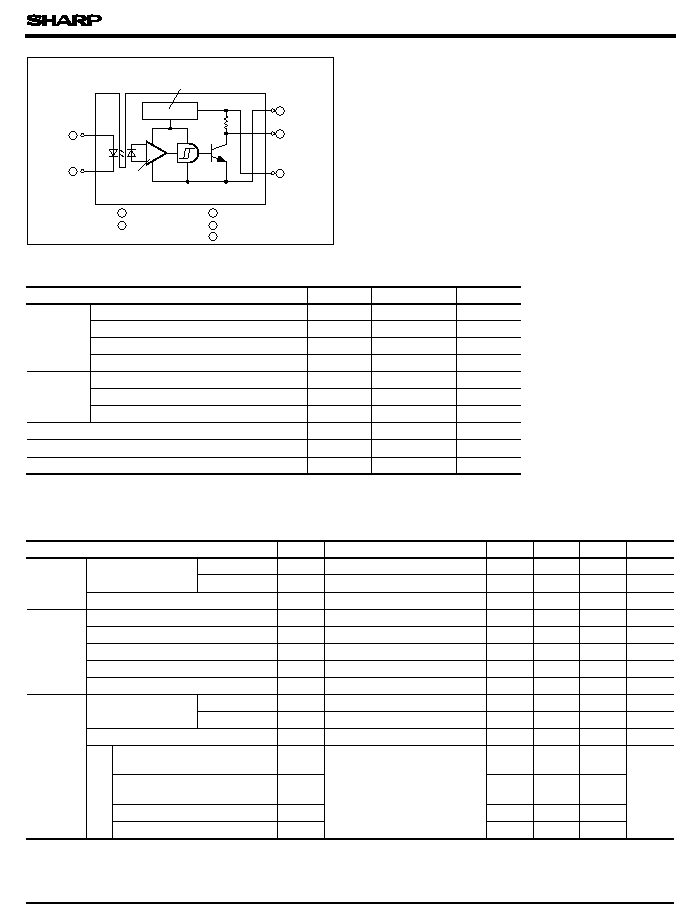
3.
An OPIC consists of a light-detecting element and signal-
processing circuit integrated onto a single chip.
*" OPIC" ( Optical IC ) is a trademark of the SHARP Corporation.
data books, etc. Contact SHARP in order to obtain the latest version of the device specification sheets before using any SHARP's device.
"
"
In the absence of confirmation by device specification sheets, SHARP takes no responsibility for any defects that occur in equipment using any of SHARP's devices, shown in catalogs,
19.0
±
0.2
2
-
3.2
±
0.2
25.0
±
0.3
12.2
±
0.3
3.0
+
0.2
-
0.1
9.0
MIN.
5
-
0.4
+
0.3
-
0.1
5
-
0.45
+
0.3
-
0.1
5
-
0.4
+
0.3
-
0.1
5
-
0.45
+
0.3
-
0.1
3.0
+
0.2
-
0.1
2
-
3.2
±
0.2
12.2
±
0.3
9.0
MIN.
13.7
±
0.3
10.0
MIN.
5
-
0.4
+
0.3
-
0.1
5
-
0.45
+
0.3
-
0.1
5.0
+
0.2
-
0.1
5
-
0.45
+
0.3
-
0.1
5
-
0.4
+
0.3
-
0.1
3.0
+
0.2
-
0.1
12.2
±
0.3
9.0
MIN.
GP1A53HR
(Gap: 5mm )
GP1A50HR/GP1A51HR/GP1A52HR/GP1A53HR
s
Absolute Maximum Ratings
(Ta= 25∞C )
*1 Pulse width<=100
µ
s, Duty ratio= 0.01
*2 For 5 seconds
s
Electro-optical Characteristics
(Ta = 25∞C )
*5
GP1A53HR
Condition of V
OH
, I
CCH
, Response time; I
F
= 8mA
Parameter
Symbol
Rating
Unit
Input
Forward current
I
F
50
mA
*1
Peak forward current
I
FM
1
A
Reverse voltage
V
R
6
V
Power dissipation
P
75
mW
Output
Operating temperature
Supply voltage
V
CC
- 0.5 to + 17
V
Output current
I
O
50
mA
Power dissipation
P
O
250
mW
T
opr
- 25 to + 85
∞C
Storage temperature
T
stg
- 40 to + 100
∞C
*2
Soldering temperature
T
sol
260
∞C
*3 I
FLH
represents forward current when output changes from low to high.
*4 I
FHL
represents forward current when output changes from high to low. Hysteresis stands for I
FHL
/I
FLH.
Internal connection diagram
Voltage regulator
Amp
1
2
3
4
5
1 Anode
2 Cathode
3 V
CC
4 V
O
5 GND
Parameter
Symbol
Conditions
MIN.
TYP.
MAX.
Unit
Input
Output
Transfer
charac-
teristics
Forward voltage
GP1A52HR
V
F
I
F
= 5mA
-
1.1
1.4
V
GP1A53HR
V
F
I
F
= 8mA
-
1.14
1.4
V
Reverse current
I
R
V
R
= 3V
-
-
10.0
µ
A
V
CC
4.5
-
17.0
V
Low level output voltage
V
OL
V
CC
= 5V, I
F
= 0, I
OL
= 16mA
-
0.15
0.4
V
High level output voltage
V
OH
4.9
-
-
V
Low level supply current
I
CCL
V
CC
= 5V, I
F
= 0
-
1.7
3.8
mA
High level supply current
I
CCH
-
0.7
2.2
mA
*3
" Low
High"
threshold input current
GP1A52HR
I
FLH
V
CC
= 5V
-
1.0
5.0
mA
GP1A53HR
I
FLH
V
CC
= 5V
-
1.5
8.0
mA
*4
Hysteresis
I
FHL
/I
FLH
V
CC
= 5V
0.55
0.75
0.95
" Low
High"
propagation delay time
t
PLH
R
L
= 280
3.0
9.0
µ
s
-
-
5.0
15.0
" High
Low"
propagation delay time
t
PHL
-
0.1
0.5
time
Response
Rise time
t
r
-
0.05
0.5
Fall time
t
r
GP1A50HR/GP1A51HR
Operating supply voltage
GP1A50HR/GP1A51HR
V
CC
= 5V,
*5
I
F
= 5mA
V
CC
= 5V,
*5
I
F
= 5mA
V
CC
= 5V,
*5
I
F
= 5mA
(15k
)

GP1A50HR/GP1A51HR/GP1A52HR/GP1A53HR
s
Recommended Operating Conditions
Parameter
Symbol
Operating temp.
MIN.
MAX.
Unit
Low level output current
I
OL
Ta = 0 to + 70∞C
-
16.0
mA
Forward current
I
F
10.0
20.0
mA
0
10
20
30
40
50
60
100
75
50
25
0
85
- 25
- 25
85
0
25
50
75
100
300
250
200
150
100
50
0
- 25∞C
0∞C
25∞C
50∞C
1
2
5
10
20
50
100
200
500
3
2.5
2
1.5
1
0.5
0
0
100
75
50
25
0
85
- 25
60
50
40
30
20
10
0
3.5
Fig. 1 Forward Current vs. Ambient
Temperature
Fig. 2 Output Power Dissipation vs.
Ambient Temperature
Fig. 3 Low Level Output Current vs.
Ambient Temperature
Fig. 4 Forward Current vs. Forward Voltage
Forward current I
F
(
mA
)
Ambient temperature T
a
(∞C)
Output power dissipation P
O
(
mW
)
Ambient temperature T
a
( ∞C)
Low level output current I
OL
(
mA
)
Ambient temperature T
a
(∞C)
Forward current I
F
(
mA
)
Forward voltage V
F
( V)
T
a
= 75∞C

GP1A50HR/GP1A51HR/GP1A52HR/GP1A53HR
0
5
10
15
20
1.1
1.0
0.9
0.8
0.7
0.6
0.5
1.4
1.2
1.0
0.8
0.6
0.4
0
50
40
0
30
20
10
2
4
8
6
5mA
16mA
- 25
0
25
50
75
100
0.4
0.3
0.2
0
0.1
0.5
0.6
1
10
100
2
5
20
50
1.0
0.5
0.2
0.1
0.01
0.02
0.05
5V
10V
- 25
0
25
50
75
100
2.0
1.5
1.0
0
0.5
2.5
3.0
25
1.6
10V
5V
}
}
60
Fig. 5 Relative Threshold Input Current vs.
Supply Voltage
Fig. 6 Relative Threshold Input Current vs.
Ambient Temperature
Fig. 7 Low Level Output Voltage vs.
Low Level Output Current
Fig. 8 Low Level Output Voltage vs.
Ambient Temperature
Fig. 9 Supply Current vs. Ambient Temperature
I
FLH
I
FHL
I
FLH
= 1 at V
CC
= 5V
T
a
= 25∞C
Supply voltage V
CC
( V)
V
CC
= 5V
I
FLH
I
FHL
I
FLH
= 1 at T
a
= 25∞C
V
CC
= 5V
T
a
= 25∞C
Low level output current I
OL
( mA )
V
CC
= 5V
I
OL
= 30mA
Supply current I
CC
(
mA
)
Ambient temperature T
a
(∞C)
Forward current I
F
( mA )
Propagation delay time t
PLH
, t
PHL
(
µ
s
)
t
PLH
V
CC
= 17V
I
CCL
I
CCH
V
CC
= 17V
V
CC
= 5V
R
L
= 280
T
a
= 25∞C
t
PHL
12
10
Ambient temperature T
a
( ∞C)
Relative threshold input current I
FHL
, /I
FLH
Relative threshold input current I
FHL
/ I
FLH
- 25
0
25
50
75
100
Low level output voltage V
OL
(
V
)
Low level output voltage V
OL
(
V
)
Fig.10-a Propagation Delay Time vs. Forward Current
(GP1A50HR/GP1A51HR/GP1A52HR )
Ambient temperature T
a
( ∞C)

GP1A50HR/GP1A51HR/GP1A52HR/GP1A53HR
60
6
8
4
10
2
12
10
20
30
0
40
50
0
0.1
50
20
0.6
0.7
0.8
0.2
1
10
0.5
2
5
0.5
0.4
0.3
0
0.1
0.2
10%
90%
50%
1.5V
Input
Output
Input
47
Voltage regulator
Amp.
+
5V
Output
0.01
µ
F
280
Test Circuit for Response Time
GND
V
CC
= 5V
R
L
= 280
T
a
= 25∞C
t
PHL
t
PLH
Propagation delay time t
PLH
,t
PHL
(
µ
s
)
Forward current I
F
( mA )
(GP1A53HR)
T
a
= 25∞C
V
CC
= 5V
I
F
= 5mA
Rise time, fall time t
r
,t
f
(
µ
s
)
Load resistance R
L
( k
)
t
r
t
f
I
F
=
5mA
t
r
=t
f
=0.01
µ
s
t
PLH
t
r
t
PHL
V
OH
V
OL
t
f
Fig.12 Rise Time, Fall Time vs.
Load Resistance
s
Precautions for Use
Fig.10-b Propagation Delay Time vs.
Forward Current
( 1) In order to stabilize power supply line, connect a by-pass capacitor of more than 0.01
µ
F
between Vcc and GND near the device.
( 2) In case of cleaning, use only the following type of cleaning solvent.
Ethyl alcohol, Methyl alcohol, Isopropyl alcohol
(15k
)
Z
O
=50
( 3) As for other general cautions refer to the chapter " Precautions for Use " .