GP1S38/GP1S381
GP1S38/GP1S381
s
Applications
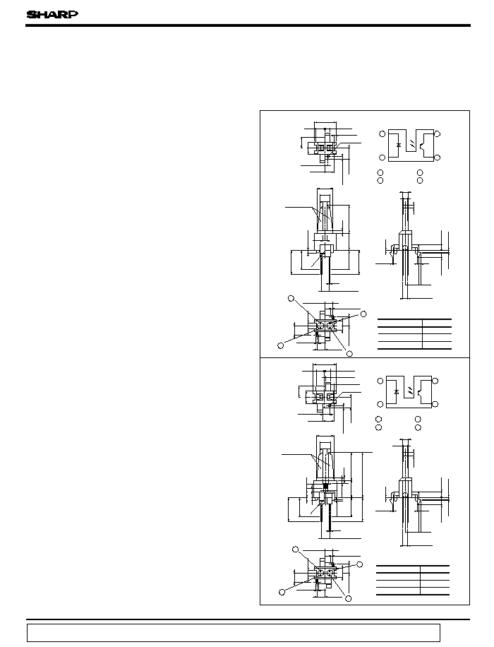
(Unit : mm )
s
Features
s
Outline Dimensions
that can be devided into Assy substrate
( mather substrate )
without leads, connectors, etc.
3. Easy mounting to PWB due to the holder
with hook
4. Gap between light emitter and detector:
1.2
8.9
(
12.6
)
(
14.6
)
(
14.6
)
(
12.6
)
2
-
1.5
4.9
3.2
3
0.2
2
-
0.3
*
( 2.54 )
2
-
7
2
-
1
2
-
1
2
-
0.3
2
-
3.0
3
-
3.45
(Transparency)
RO.5
2
-
0.9
6.5
6
5.75
(
1.5
)
5
2
1.2
8.9
2
-
1.5
1.8
*(
3.85
)
4.9
3.2
1.5
2
3
0.2
2
-
0.3
*( 2.54 )
2
-
7
2
-
1
2
-
1
2
-
0.3
2
-
3.0
3
-
3.45
(Transparency)
RO.5
2
-
0.9
2
-
2.5
11
4.5
6.5
6
5.75
(
1.5
)
4.25
( 1.5 )
Internal connection diagram
1 Anode
2 Collector
3 Emitter
4 Cathode
4
1
3
2
Internal connection diagram
1 Anode
2 Collector
3 Emitter
4 Cathode
4
1
3
2
Dimensions(d) Tolerance
d
<
5.0
�
0.2
5.0
<=
d
<
15.0
�
0.25
15.0
<=
d
�
0.3
5
12
2
-
2.5
2
-
3
( 2.5 )
5.25
(7.16)
2.8
5.5
�
0.1
4.5
�
0.1
5
�
0.1
2
-
1.5
2-2
2.1
1.8
2
-
1.5
Max. 0.4
1. Optical guide for setting detecting position
2. PWB mounting type
( 12.6
)
( 14.6
)
( 12.6
)
( 14.6
)
*
Unspecified tolerances
shall be as follows
;
*
( )
:
Reference dimensions
1
2
3
4
3
11.6
*
( 4.85 )
1
2
3
4
*
Unspecified tolerances
shall be as follows
;
*
( )
:
Reference dimensions
GP1S38
Optical Guide Photointerrupter
Optical guide
GP1S381
Optical guide
1. VCRs
GP1S38
:2mm
GP1S381
:3mm
data books, etc. Contact SHARP in order to obtain the latest version of the device specification sheets before using any SHARP's device.
"
"
In the absence of confirmation by device specification sheets, SHARP takes no responsibility for any defects that occur in equipment using any of SHARP's devices, shown in catalogs,
(
1) Hole
8.3
+
0
-
0.1
14.5
+
0
-
0.2
2
-
1.65
+
0.05
-
0
0.5
+
0.15
-
0.1
3.5
+
0.1
-
0.1
1.5
+
0.1
-
0.1
5
+
0.1
-
0.1
4
+
0.1
-
0.1
1
+
0.1
-
0.1
5.5
+
0.1
-
0.1
(
1) Hole
8.9
+
0
-
0.1
20.5
�
0.15
0.5
+
0.15
-
0.1
2
-
1.65
+
0.05
-
0
1.5
+
0
-
0.05
4
+
0.1
-
0.1
1
+
0
-
0.05
Dimensions(d) Tolerance
d
<
5.0
�
0.2
5.0
<=
d
<
15.0
�
0.25
15.0
<=
d
�
0.3
GP1S38/GP1S381
Parameter
Symbol
Rating
Unit
Input
Forward current
I
F
60
mA
*1
Peak forward current
I
FM
1
A
Reverse voltage
V
R
6
V
Power dissipation
P
150
mW
Output
Collector-emitter voltage
V
CEO
35
V
Emitter-collector voltage
V
ECO
6
V
Collector current
I
C
20
mA
Collector power dissipation
P
C
50
mW
T
opr
- 25 to + 80
�C
Storage temperature
T
stg
- 40 to + 80
�C
*2
Soldering temperature
T
sol
260
�C
s
Absolute Maximum Ratings
(Ta = 25�C )
(Ta = 25�C )
s
Electro-optical Characteristics
*1 Pulse width <= 100
�
s, Duty ratio: 0.01
Vcc
Measuring terminal
Input
Output
10
%
90
%
tr
tf
s
Test Circuit for Response Time
Operating temperature
R
L
*2 3 seconds or less at the position of 1mm or more from the surface of resin
Parameter
Symbol
Conditions
MIN.
TYP.
MAX.
Unit
Input
Forward voltage
V
F
I
F
= 50mA
-
-
1.5
V
Peak forward voltage
V
FM
I
FM
= 0.5A
-
-
3.5
V
Reverse current
I
R
V
R
= 3V
-
-
10
�
A
Output
Collector dark current
I
CEO
V
CE
= 20V
-
-
100
nA
Transfer
charac-
teristics
Collector current
I
C
V
CE
= 5V, I
F
= 20mA
100
-
-
�
A
Collector-emitter saturation voltage
V
CE( sat )
I
F
= 40mA, I
C
= 30
�
A
-
-
0.4
V
Response time
Rise time
t
r
V
CE
= 10V, I
C
= 50
�
A
R
L
= 100k
-
0.85
2.5
ms
Fall time
t
f
-
0.75
2.1
ms

GP1S38/GP1S381
0
25
50
75
0
50
40
30
20
16
10
100
80
60
70
Fig. 1 Forward Current vs.
Ambient Temperature
F
(
mA
)
- 25
Ambient temperature T
a
(�C)
0
25
50
75
0
60
50
40
20
22.5
100
80
80
100
Fig. 2 Collector Power Dissipation vs.
Ambient Temperature
- 25
Ambient temperature T
a
(�C)
Collector power dissipation P
C
(
mW
)
2
5
20
200
100
50
500
1000
2000
2
5
2
5
Fig. 3 Peak Forward Current vs.
Duty Ratio
10
- 3
10
- 2
10
-
1
10
0
Duty ratio
Peak forward current I
FM
(
mA
)
500
200
100
50
20
10
5
2
3.5
3.0
2.5
2.0
1.5
1.0
0.5
1
0
Forward voltage V
F
(V)
Forward current I
F
(
mA
)
Forward Voltage
50�C
25�C
0�C
Fig. 4 Forward Current vs.
60
54
48
42
30
24
18
0
0
6
1.0
2.0
3.0
4.0
5.0
12
36
Forward Current
V
CE
= 5V
T
a
= 25�C
Forward current I
F
( mA )
Collector current I
C
(
mA
)
8
6
4
5.0
4.0
3.0
2.0
1.0
10
2
0
0
I
F
= 60mA
T
a
= 25�C
CE
(V)
Collector current I
C
(
mA
)
- 20�C
Forward current I
50mA
40mA
30mA
20mA
10mA
Fig. 6 Collector Current vs.
Fig. 5 Collector Current vs.
Collector-emitter Voltage
Collector-emitter voltage V
width<=100 ms
Pulse
T
a
= 25�C
T
a
= 75�C

GP1S38/GP1S381
0
25
50
75
0
1.0
0.8
0.6
0.4
0.2
100
1.2
1.4
Fig. 7 Collector Current vs.
Ambient Temperature
Collector current I
C
(
mA
)
- 25
I
F
= 20mA
V
CE
= 5V
0
25
50
75
0
0.10
0.08
0.06
0.04
0.02
100
0.12
Ambient Temperature
I
F
= 40mA
I
C
= 30mA
- 25
CE
( sat
)
(
V
)
Ambient temperature T
a
(�C)
0.1
1
10
1
1000
100
10
100
0.01
Fig. 9 Response Time vs.
V
CE
= 10V
I
C
= 50mA
T
a
= 25�C
L
( k
)
10
- 7
10
- 8
10
- 9
10
- 10
0
25
50
75
100
2
5
2
5
2
5
2
5
Ambient Temperature
10
- 6
- 25
V
CE
= 20V
Ambient temperature T
a
(�C)
Collector dark current I
CEO
(
A
)
Fig.10 Collector Dark Current vs.
L
1
2
3
4
5
6
7
10
20
30
40
50
60
70
80
90
100
Fig.11 Relative Collector Current vs.
Shield Distance ( 1 )
L
10
20
30
40
50
60
70
80
90
100
0
1
2
3
Fig.12 Relative Collector Current vs.
Shield Distance ( 2 )
Fig. 8 Collector-emitter Saturation Voltage vs.
Collector-emitter saturation voltage V
Response time
(ms
)
(GP1S38 )
Shield distance (1) L ( mm )
(GP1S38 )
Shield distance (2) L ( mm )
Shield
Shield
Relative collector current
(
%
)
Relative collector current
(
%
)
Ambient temperature T
a
( �C )
t
f
t
r
t
d
t
s
Load Resistance
Load resistance R

GP1S38/GP1S381
1
2
3
4
5
6
7
10
20
30
40
50
60
70
80
90
100
Shield Distance ( 1 )
Fig.13 Relative Collector Current vs.
L
10
20
30
40
50
60
70
80
90
100
0
1
2
3
Shield Distance ( 2 )
Fig.14 Relative Collector Current vs.
L
( GP1S381)
( GP1S381)
Relative collector current
(
%
)
Relative collector current
(
%
)
Shield distance (1) L ( mm )
Shield distance (2) L ( mm )
Shield
Shield
q
Please refer to the chapter " Precautions for Use" .