 | –≠–ª–µ–∫—Ç—Ä–æ–Ω–Ω—ã–π –∫–æ–º–ø–æ–Ω–µ–Ω—Ç: GP1S51V | –°–∫–∞—á–∞—Ç—å:  PDF PDF  ZIP ZIP |

GP1S50/GP1S51V
GP1S52V/GP1S54
s
Features
1. High sensing accuracy ( Slilt width : 0.5mm )
s
Applications
1. OA equipment, such as FDDs, printers,
facsimiles
2. VCRs
s
Outline Dimensions
(Unit : mm )
GP1S50/GP1S51V/GP1S52V/GP1S54
GP1S50
(Case height : 10mm )
Either-side mounting type :
GP1S51V
(Case height : 10mm )
PWB direct mounting type :
GP1S52V
PWB direct mounting type :
GP1S54
0.5
(9.2)
(2.54)
2
-
C2.0
6.0
5.0
1.5
7.5
10.0
7.0
3.5
Slit width
GP1S50
GP1S54
1.5
3.5
(9.2)
(2.54)
0.5
Slit width
10.0
5.0
C1.0
7.5
2.5
C1.0
Slit width
0.5
5.0
(2.54)
8.0
2
-
0.7
6.0
( 2.5
)
Detector center
(9.2)
1.75
4.2
3.5
1.5
7.5
2.5
(9.2)
(2.54)
5.0
7.0
12.0
18.0
6.0
10.0
3
2
1
4
1
4
3
2
4 3
2
1
GP1S51V
(Both sides of
detector and
emitter )
Marking
:
GP1S50
Dimensions(d) Tolerance
d
<=
6.0
±
0.1
6.0
<
d
<=
18.0
±
0.2
18.0
<
d
<=
25.0
±
0.25
(Both sides of
detector and
emitter )
Dimensions(d) Tolerance
d
<=
6.0
±
0.1
6.0
<
d
<=
18.0
±
0.2
(Both sides of
detector and
emitter )
GP1S52V
Dimensions(d) Tolerance
d
<=
6.0
±
0.1
6.0
<
d
<=
18.0
±
0.2
(Both sides of
detector and
emitter )
GP1S54
Dimensions(d) Tolerance
d
<=
6.0
±
0.1
6.0
<
d
<=
18.0
±
0.2
General Purpose
Photointerrupter
Both-sides mounting type :
2.
(Case height : 10mm )
(Case height : 8mm )
2.0
S51
5
3
+
0.2
-
0.1
12.2
+
0.3
-
0.3
1
2
3
4
5
12.2
+
0.3
-
0.3
3
+
0.2
-
0.1
S52
*
Unspecified tolerances shall be as follows
;
*
( )
:
Reference dimensions
*
Unspecified tolerances shall be as follows
;
*
( )
:
Reference dimensions
*
Unspecified tolerances shall be as follows
;
*
( )
:
Reference dimensions
*
Unspecified tolerances shall be as follows
;
*
( )
:
Reference dimensions
data books, etc. Contact SHARP in order to obtain the latest version of the device specification sheets before using any SHARP's device.
"
"
In the absence of confirmation by device specification sheets, SHARP takes no responsibility for any defects that occur in equipment using any of SHARP's devices, shown in catalogs,
Slit width
0.5
19.0
±
0.2
2
-
3.2
±
0.2
25.0
±
0.3
12.2
±
0.3
3.0
+
0.2
-
0.1
10.0
MIN.
4
-
0.4
+
0.3
-
0.1
4
-
0.45
+
0.3
-
0.1
10.0
MIN.
12.2
±
0.3
3.0
+
0.2
-
0.1
4
-
0.4
+
0.3
-
0.1
4
-
0.45
+
0.3
-
0.1
2
-
3.2
±
0.2
12.0
MIN.
12.2
±
0.3
3.0
+
0.4
-
0
4
-
0.4
+
0.3
-
0.1
4
-
0.45
+
0.3
-
0.1
2
-
R0.3
MAX.
7.5
±
0.1
2
-
0.7
3.0
+
0.2
-
0.1
4
-
0.4
+
0.3
-
0.1
4
-
0.45
+
0.3
-
0.1
10.0
MIN.
12.2
±
0.3

GP1S50/GP1S51V/GP1S52V/GP1S54
Parameter
Symbol
Rating
Unit
Input
Forward current
I
F
50
mA
*1
Peak forward current
I
FM
1
A
Reverse voltage
V
R
6
V
Power dissipation
P
75
mW
Output
Collector-emitter voltage
V
CEO
35
V
Emitter-collector voltage
V
ECO
6
V
Collector current
I
C
20
mA
Collector power dissipation
P
C
75
mW
Operating temperature
T
opr
- 25 to + 85
∞C
Storage temperature
T
stg
- 40 to + 100
∞C
*2
Soldering temperature
T
sol
260
∞C
s
Absolute Maximum Ratings
(Ta = 25∞C )
*1 Pulse width<=100
µ
s, Duty ratio= 0.01
*2 For 5 seconds
1
2
4
3
1 Anode
2 Cathode
3 Collector
4 Emitter
Internal connection diagram (Common to 4 models )
s
Electro-optical Characteristics
(Ta = 25∞C )
Parameter
Symbol
Conditions
MIN.
TYP.
MAX.
Unit
Input
Output
Forward
voltage
GP1S50/ GP1S51V/ GP1S52V
V
F
I
F
= 20mA
-
1.25
1.4
V
GP1S54
-
1.2
1.4
Peak forward voltage
V
FM
I
FM
= 0.5A
-
3
4
V
Reverse current
I
R
V
R
= 3V
-
-
µ
A
Transfer
charac-
teristics
Collector dark current
I
CEO
V
CE
= 20V
-
I
F
= 20mA, V
CE
= 5V
0.5
-
5
mA
Collector-emitter saturation voltage
V
CE ( sat )
I
F
= 40mA, I
C
= 0.5mA
-
-
0.4
V
Response time
Rise time
t
R
V
CE
= 2V, I
CE
= 2mA
R
L =
100
-
3
15
µ
s
Fall time
t
F
-
4
20
µ
s
10
1
100
nA
Collector Current
Ic

- 25
0
25
50
75
100
0
10
20
30
40
50
60
85
- 25
0
25
50
75
100
0
20
40
60
85
80
100
120
75
0
0.5
1
1.5
2
1
2
10
20
100
200
2.5
3
5
50
500
25∞C
0∞C
- 25∞C
50∞C
20
5
5
2
5
2
50
100
200
500
3.5
0
20
0
10
10
8
6
4
2
30
40
0
2
0
2
4
6
8
10
4
6
40mA
30mA
20mA
10mA
50
12
Duty ratio
1
3
5
7
9
1
3
5
7
Fig. 1 Forward Current vs. Ambient
Temperature
Fig. 2 Collector Power Dissipation vs.
Ambient Temperature
Fig. 3 Peak Forward Current vs.
Duty Ratio
Fig. 4 Forward Current vs.
Forward Voltage
Fig. 5 Collector Current vs.
Forward Current
Fig. 6 Collector Current vs.
Collector-emitter Voltage
Forward current I
F
(
mA
)
Ambient temperature T
a
(∞C)
Collector power dissipation P
C
(
mW
)
Ambient temperature T
a
(∞C)
Peak forward current I
FM
(
mA
)
T
a
= 75∞C
Forward current I
F
(
mA
)
F
(V)
Collector current I
C
(
mA
)
Forward current I
F
( mA )
T
a
= 25∞C
I
F
= 50mA
Collector current I
C
(
mA
)
Collector-emitter voltage V
CE
(V)
GP1S50/GP1S51V/GP1S52V/GP1S54
V
CE
= 5V
T
a
= 25∞C
T
a
= 25∞C
Forward voltage V
10
- 2
10
- 1
Pulse width <=100
µ
s
2000
1000
1
Response time
(
µ
s
)
0.01
10
%
Test Circuit for Response Time
Output
Input
90
%
Input
Output
0.02
0.05 0.1 0.2
0.5
1
2
5
10
0.1
0.2
0.5
1
2
5
10
20
100
0
25
50
75
100
2
5
2
5
2
5
2
5
Fig.10 Frequency Response
Frequency f ( Hz )
2
0
5
5
2
5
2
5
2
10k
1k
100
4.0
0
25
50
75
100
3.5
3.0
2.5
2.0
1.5
1.0
0.5
0
0
100
75
50
25
0
Collector-emitter saturation voltage
0.05
0.1
0.15
0.2
0.25
Fig. 7 Collector Current vs.
Ambient Temperature
Fig. 8 Collector-emitter Saturation Voltage vs.
Ambient Temperature
Fig. 9 Response Time vs.
Fig.11 Collector Dark Current vs.
Ambient Temperature
Collector current I
C
(
mA
)
Ambient temperature T
a
(∞C)
I
F
= 40mA
I
C
= 0.5mA
Ambient temperature T
a
(∞C)
t
f
t
r
t
d
t
s
L
( k
)
50
R
D
V
CC
R
L
t
d
t
r
t
s
t
f
Voltage gain A
V
(
dB
)
V
CE
= 20V
Collector dark current I
CEO
(
A
)
Ambient temperature T
a
(∞C)
GP1S50/GP1S51V/GP1S52V/GP1S54
I
F
= 20mA
V
CE
= 5V
V
CE
= 2V
I
C
= 2mA
T
a
= 25∞C
V
CE
= 2V
I
C
= 2mA
T
a
= 25∞C
V
CE
(
sat
)
(V
)
10
3
10
4
10
5
10
6
R
L
=
- 25
- 25
- 5
- 10
- 15
- 20
10
- 10
10
- 9
10
- 8
10
- 7
10
- 6
- 25
Load Resistance
Load resistance R
- 1.5
0
0.5
0
Relative collector current
(
%
)
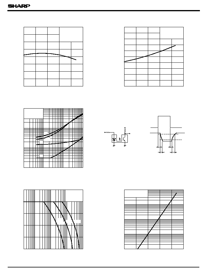
Shield distance L ( mm )
- 1.0 - 0.5
2.5
50
100
(Detector center )
Detector
Shield
L
0
+
-
-
+
0
L
Shield
Detector
(Detector center
)
Shield distance L ( mm )
Relative collector current
(
%
)
2.0
1.5
1.0
100
50
- 1
- 2
0
1
0
- 3
2
3
4
5
Fig.13 Relative Collector Current vs.
Shield Distance ( 2 )
Fig.12 Relative Collector Current vs.
Shield Distance ( 1 )
I
F
= 20mA, V
CE
= 5V
T
a
= 25∞C
I
F
= 20mA, V
CE
= 5V
T
a
= 25∞C
s
Precautions for Use
GP1S50/GP1S51V/GP1S52V/GP1S54
( 1) In case of cleaning, use only the following type of cleaning solvent.
Ethyl alcohol, methyl alcohol, Isopropyl alcohol
( 2) Please refer to the chapter " Precautions for Use " .