GP1S562
s Applications
s
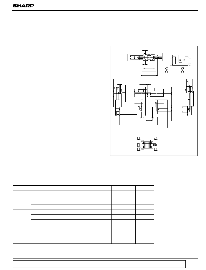
Outline Dimentions
s
Absolute Maximum Ratings
( Unit : mm)
*1 Pulse width<=100
µ
s, Duty ratio : 0.01
( Ta = 25∞C)
GP1S562
1. Compact package
2. With a spacer
3. With a hook for temporary
installation to PWB
1. Floppy disk drivers
*2 For 5 seconds
2
3
4
1
6.2
4
-
3.8
(2.54)
1.5
2.2
3
5.2
1
10
12
1
2
-
1
MIN.4.5
(4.75)
0.5
2
-
0.8
4.2
1
( Top of Hook )
( Slit width )
0.3
3
7
±
0.3
2
-
5
2.1
2
-
1.4
2
-
3.4
9.6
2.4
( 3.4
)
(
Center of
sensor
)
1
2
3
4
Internal connection diagram
1 Anode
2 Cathode
4 Collector
3 Emitter
1.5
1
0.1
0.6
Parameter
Symbol
Rating
Unit
Input
Forward current
I
F
50
mA
*1
Peak forward current
I
FM
1
A
Reverse voltage
V
R
6
V
Power dissipation
P
75
mW
Output
Collecotr-emitter voltage
V
CEO
35
V
Emitter-collector voltage
V
ECO
6
V
Collector current
I
C
20
mA
Collector power dissipation
P
C
75
mW
T
opr
∞C
Storage temperature
T
stg
∞C
*2
Soldering temperature
T
sol
260
∞C
Operating temperature
Compact Photointerrupter with
Holders
s Features
*
Unspecified tolerance
:±
0.2mm
*
( )
:
Reference dimensions
*
Please be careful not to receive
external disturbing light because
the top and back face of emitter
and detector elements are not
covered by case.
2. VCRs
- 25 to + 85
- 40 to + 100
data books, etc. Contact SHARP in order to obtain the latest version of the device specification sheets before using any SHARP's device.
"
"
In the absence of confirmation by device specification sheets, SHARP takes no responsibility for any defects that occur in equipment using any of SHARP's devices, shown in catalogs,
2
-
0.8
±
0.1
8.4
+
0.1
-
0.2
4.7
+
0.2
-
0.3
0.5
+
0.4
-
0.2
4
-
0.45
+
0.3
-
0.2
12
+
0.3
-
0.4
4
-
0.25
+
0.3
-
0.2
GP1S562
(Ta = 25∞C)
s
Electro-optical Characteristics
Parameter
Symbol
Condition
MIN.
TYP.
MAX.
Unit
Input
Forward voltage
V
F
I
F
= 20mA
-
1.25
1.4
V
Peak forward voltage
V
FM
-
3
4
V
Reverse current
I
R
V
R
= 3V
-
-
10
µ
A
Output
I
CEO
V
CE
= 20V
-
1
100
nA
Transfer
Collector current
I
C
V
CE
= 5V, I
F
= 20mA
1.4
-
8.5
mA
Collector-emitter saturation voltage
V
CE( sat )
I
F
= 40mA, I
C
= 1.4mA
-
-
0.4
V
Rise time
t
r
V
CE
= 2V, I
C
= 2mA
R
L
= 100
-
3
15
Fall time
t
f
-
4
20
Response time
I
FM
= 0.5A
µ
s
µ
s
- 25
0
25
50
75
85
100
0
10
20
30
40
50
60
- 25
0
25
50
75
85
100
0
20
15
40
60
80
100
120
75
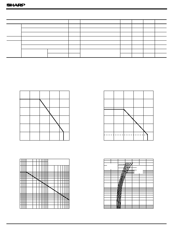
Fig. 1 Forward Current vs.
Ambient Temperature
Fig. 2 Collector Power Dissipation vs.
Ambient Temperature
Forward current I
F
(
mA
)
Ambient temperature T
a
(∞C)
Collector power dissipation P
C
(
mW
)
Ambient temperature T
a
(∞C)
Collector dark current
charac-
teristics
1000
2000
500
200
100
50
20
5
2
5
2
5
Duty ratio
Pulse width <=100
µ
s
Peak forward current I
FM
(
mA
)
T
a
= 25∞C
Duty Ratio
Fig. 3 Peak Forward Current vs.
10
- 2
10
- 1
0
1
0.5
1.0
1.5
2.0
2.5
3.0
3.5
2
5
10
20
50
100
200
500
Forward current I
F
(
mA
)
Forward voltage V
F
(V)
Fig. 4 Forward Current vs. Forward Voltage
25∞C
0∞C
50∞C
T
a
= 75∞C
- 20∞C
1
GP1S562
0
0
20
16
12
8
4
10
8
6
4
2
V
CE
= 5V
T
a
= 25∞C
Forward current I
F
( mA )
Collector current I
C
(
mA
)
0
0
2
4
6
8
10
2
4
6
8
10
T
a
= 25∞C
I
F
= 50mA
CE
(V)
Collector current I
C
(
mA
)
0
25
50
0
2
1
75 85
3
4
- 25
Ambient temperature T
a
(∞C)
Collector current I
C
0
25
50
0
Collector-emitter
0.15
0.1
75 85
0.2
Ambient Temperature
- 25
saturation voltage V
CE
( sat
)
(
V
)
Ambient temperature T
a
Voltage
Temperature
1
100
10
10
0.1
1
L
Response time
(
µ
s
)
Fig. 5 Collector Current vs. Forward Current
40mA
30mA
20mA
10mA
Fig. 6 Collector Current vs. Collector-emitter
Collector-emitter voltage V
Fig. 8 Collector-emitter Saturation Voltage vs.
( ∞C)
Fig. 7 Collector Current vs. Ambient
(
mA
)
( k
)
10
%
Test Circuit for Response Time
Output
Input
90
%
Input
Output
R
D
V
CC
R
L
t
d
t
r
t
s
t
f
V
CE
= 5V
I
C
= 2mA
T
a
= 25∞C
t
f
t
r
t
s
t
d
t
s
t
f
t
r
t
d
Fig. 9 Response Time vs. Load Resistance
Load resistance R
V
CE
=5V
I
F
=20mA
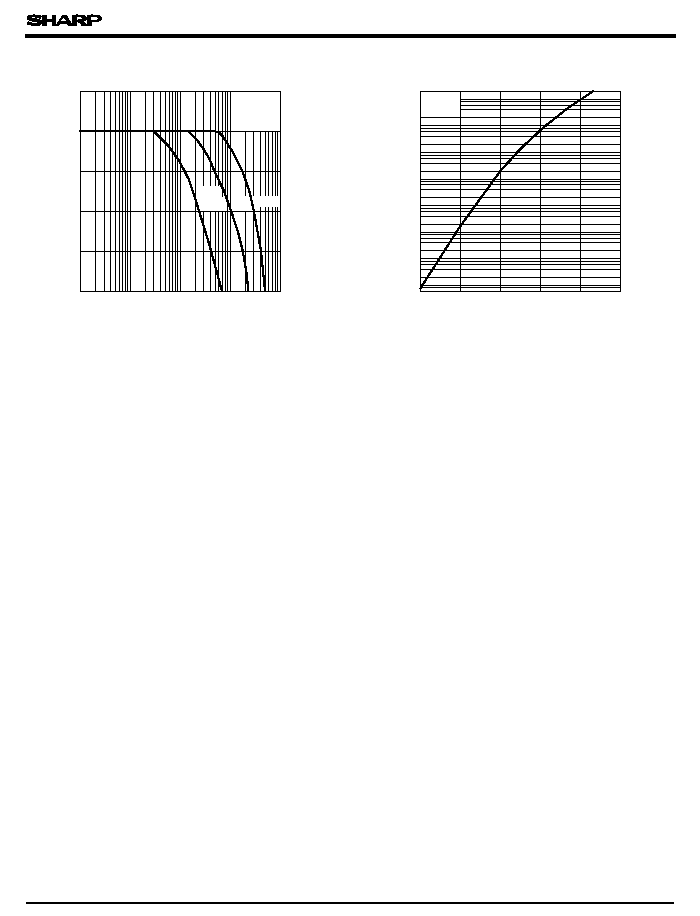
GP1S562
- 25
0
25
100
50
75
5
5
5
5
5
5
5
= 10V
5
Ambient Temperature
V
CE
Collector dark current I
CEO
(
A
)
Ambient temperature T
a
(∞C)
Fig.11 Collector Dark Current vs.
10
- 4
10
- 5
10
- 6
10
- 7
10
- 8
10
- 9
10
- 10
10
- 11
2
5
- 20
- 15
- 10
- 5
0
5
5
5
Fig.10 Frequency Response
2
2
2
10k
1k
100
V
CE
= 2V
I
C
= 10mA
R
L
=
T
a
= 25∞C
10
3
10
4
10
5
10
6
Voltage gain Av
(
dB
)
Frequency f ( Hz )
q
Please refer to the chapter "Precautions for Use ".