 | –≠–ª–µ–∫—Ç—Ä–æ–Ω–Ω—ã–π –∫–æ–º–ø–æ–Ω–µ–Ω—Ç: GP1S73P | –°–∫–∞—á–∞—Ç—å:  PDF PDF  ZIP ZIP |

(Ta=25∞C)
I
F
50
mA
I
FM
1
A
V
R
6
V
P
75
mW
V
CEO
35
V
V
ECO
6
V
I
C
20
mA
P
C
75
mW
T
opr
∞C
T
stg
∞C
±
0.15
±
0.2
±
0.3
Outline Dimensions
Features
Applications
Absolute Maximum Ratings
(Unit : mm)
1. Compact type
2. Snap-in mounting type
1. Copiers
2. Laser beam printers
3. Facsimiles
Rating
Unit
Parameter
Symbol
Input
Output
Forward current
Reverse voltage
Power dissipation
Collector-emitter voltage
Emitter-collector voltage
Collector current
Collector power dissipation
Peak forward current
*1
*
Unspecified tolerances shall be
as follows.
*
( ) : Connector dimensions for reference
Tolerance
Dimension(d)
Storage temperature
Operating temperature
- 40 to + 85
GP1S73P/GP1S74P
GP1S73P/GP1S74P
Compact Photointerrupter
with Connector
3. 3 kinds of mounting plate thickness
- 25 to + 85
*1 Pulse width 100
µ
s, Duty ratio=0.01
*2 The connector should be plugged in/out at normal temperature.
d < 5.0
5.0
<=
d < 15.0
15.0
<=
d
±
0.15
±
0.2
±
0.3
1 Collector
3 Anode
2 GND
Internal Connection Diagram (Both GP1S73P/GP1S74P)
(Applicable plate thickness : 1.0, 1.2 and 1.6 mm)
GP1S73P
GP1S74P
( 6.8 )
JAPAN AMP made
connector 175487-3
(Case surface)
13.6
(Sensor center)
(
2.3
)
7.2
5.6
1.1
0.6
0.2
2.3
4.3
4.3
6.8
±
1
5.0
2.4
(
5.8
)
3.2
1.1
2.3
5.4
6.9
9.9
11.4
14.0
16.8
0.7
17.0
1.6
4.7
2-0.9
2-0.5
4.0
2-0.5
±
0.1
(Slit)
(
7.8
)
SHARP
74
JAPAN
8.0
1 Collector
2 GND
3 Anode
( 6.8 )
JAPAN AMP made
connector 175487-3
(Case surface)
13.6
(Sensor center)
(
2.3
)
7.2
5.6
1.1
0.6
0.2
2.3
4.3
4.3
6.8
±
1
5.0
2.4
(
5.8
)
3.2
1.1
2.3
5.4
6.9
9.9
11.4
14.0
16.8
1.2
0.75
17.0
1.6
4.7
2-0.9
2-0.5
4.0
2-0.5
±
0.1
(Slit)
(
7.8
)
SHARP
73
JAPAN
8.0
1 Collector
2 GND
3 Anode
*
Unspecified tolerances shall be
as follows.
*
( ) : Connector dimensions for reference
Tolerance
Dimension(d)
d < 5.0
5.0
<=
d < 15.0
15.0
<=
d
s
s
s
s
s

V
F
-
1.2
1.4
V
V
FM
-
V
I
R
-
-
10
µ
A
I
CEO
-
1
100
nA
I
C
0.5
-
15
mA
V
CE(sat)
-
-
V
t
r
-
3
15
µ
s
t
f
-
4
20
µ
s
(Ta=25∞C)
I
F
= 20mA
I
FM
=0.5A
V
R
= 3V
V
CE
= 20V
V
CE
= 5V, I
F
= 20mA
I
F
= 40mA, I
C
= 0.5mA
V
CE
= 2V, I
C
= 2mA
R
L
= 100
- 25
0
25
50
100
0
10
20
30
40
50
60
- 25
0
25
50
75
100
0
20
40
60
80
75
20
5
5
2
5
2
50
100
200
500
1000
2000
10
-2
10
-1
75
85
1
T
a
= 25∞C
Electro-optical Characteristics
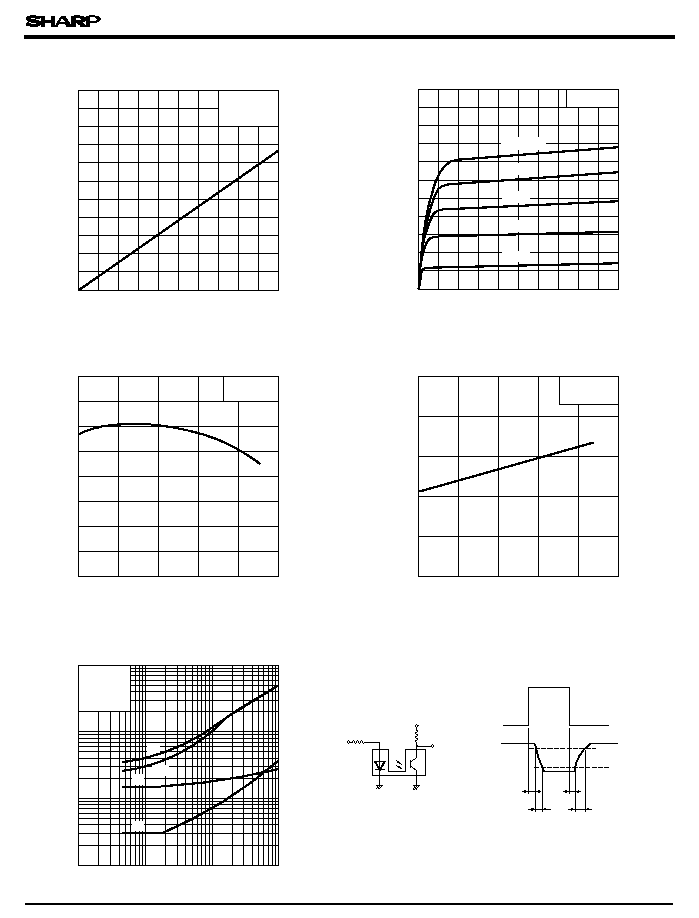
Fig. 1 Forward Current vs. Ambient
Temperature
Fig. 2 Collector Power Dissipation vs.
Ambient Temperature
Parameter
Symbol
MIN.
TYP.
MAX.
Unit
Conditions
Input
Output
Transfer
characteristics
Peak forward voltage
Reverse current
Dark current
Collector-emitter saturation voltage
Response time
Rise time
Fall time
Forward current I
F
(
mA
)
Collector power dissipation P
C
(
mW
)
Ambient temperature Ta (∞C)
Ambient temperature Ta (∞C)
Peak forward current I
FM
(mA)
Duty ratio
Pulse width <=100
µ
s
0.4
GP1S73P/GP1S74P
3.0
4.0
100
Fig. 3 Peak Forward Current vs. Duty Ratio
Fig. 4 Forward Current vs. Forward Voltage
Forward current I
F
(
mA
)
Forward voltage V
F
(V)
15
Forward voltage
Collector current
85
0
0.5
1.0
1.5
2.0
2.5
3.0
3.5
1
2
5
10
20
50
0∞C
100
200
500
1000
Ta= 85∞C
50∞C
25∞C
- 25∞C
s
Collector current Ic (mA)
Collector current Ic (mA)
Collector-emitter saturation voltage V
CE
( sat
)
(
V
)
Ambient temperature Ta (∞C)
Fig. 5 Collector Current vs. Forward Current
Collector current Ic (mA)
Forward current I
F
(mA)
Collector-emitter voltage V
CE
(V)
Fig. 7 Collector Current vs. Ambient
temperature
Ambient temperature Ta (∞C)
Fig. 8 Collector-emitter Saturation Voltage
vs. Ambient Temperature
Fig. 6 Collector Current vs. Collector-emitter
Voltage
Fig. 9 Response Time vs. Load Resistance
10
%
90
%
R
D
V
CC
R
L
t
d
t
r
t
s
t
f
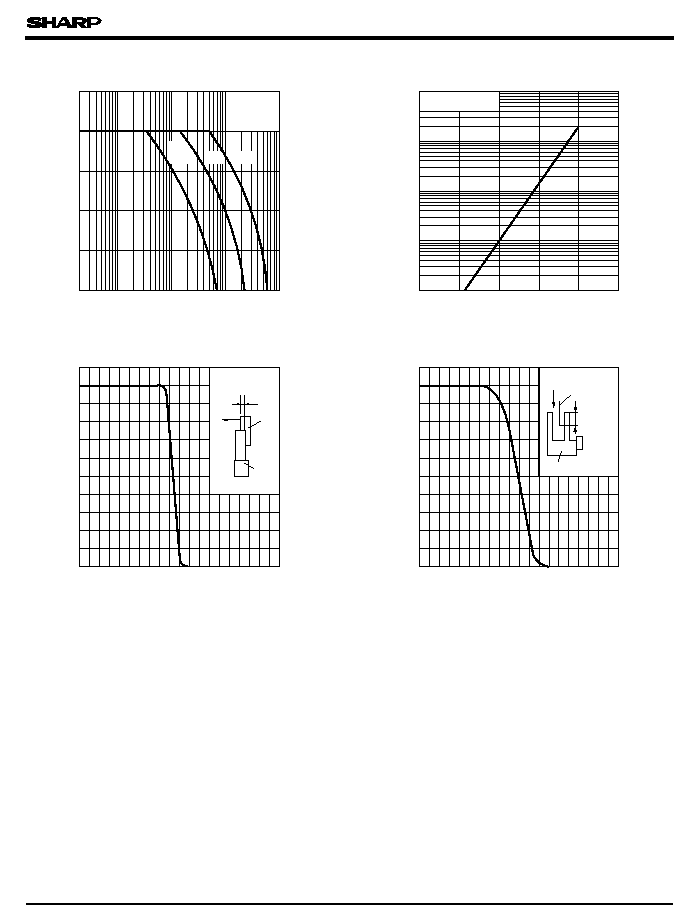
Test Circuit for Response Time
Input
Input
Output
Output
Response time (
µ
s)
Road resistance R
L
(k
)
GP1S73P/GP1S74P
0.01 0.02
0.05 0.1 0.2
0.5
1
2
5
10
0.1
0.2
0.5
1
2
5
10
20
50
100
t
s
t
d
t
r
t
f
V
CE
= 2V
I
C
= 2mA
T
a
= 25∞C
- 25
0
25
50
75
100
0
0.05
0.10
0.15
0.20
0.25
I
F
= 40mA
I
C
= 0.5mA
- 25
0
25
50
75
100
0
0.5
1.0
1.5
2.0
2.5
3.0
3.5
4.0
I
F
= 20mA
V
CE
= 5V
0
1
2
3
4
5
6
7
8
9
10
0
3
4
6
8
10
Ta= 25∞C
10mA
20mA
30mA
I
F
= 50mA
40mA
0
10
20
30
40
50
0
2
4
6
8
10
V
CE
= 5V
Ta= 25∞C
10
- 6
10
- 7
10
- 8
10
- 9
10
- 10
0
25
50
75
100
2
5
2
5
2
5
2
5
- 25
V
CE
= 20V
Dark current I
CEO
(
A
)
Ambient temperature Ta (∞C)
Fig. 10 Frequency Characteristics
Frequency f (Hz)
Voltage gain A
V
(
dB
)
Fig. 11 Dark Current vs. Ambient Temperature
Relative collector current (%)
Relative collector current (%)
Shield distance L (mm)
Shield distance L (mm)
GP1S73P/GP1S74P
2
0
5
5
2
5
2
5
2
10k
1k
100
10
3
10
4
10
5
10
6
R
L
=
- 20
- 15
- 10
- 5
V
CE
= 2V
I
C
= 2mA
T
a
= 25∞C
Fig. 12 Detecting Position Characteristics (1)
Fig. 13 Detecting Position Characteristics (2)
1
2
3
4
5
10
20
30
40
50
60
70
80
90
100
Ta = 25∞C
V
CC
= 5V
Shield plate
L
Sensor
1
2
3
4
5
10
20
30
40
50
60
70
80
90
100
Ta = 25∞C
V
CC
= 5V
L
Shield plate
Sensor
GP1S73P/GP1S74P
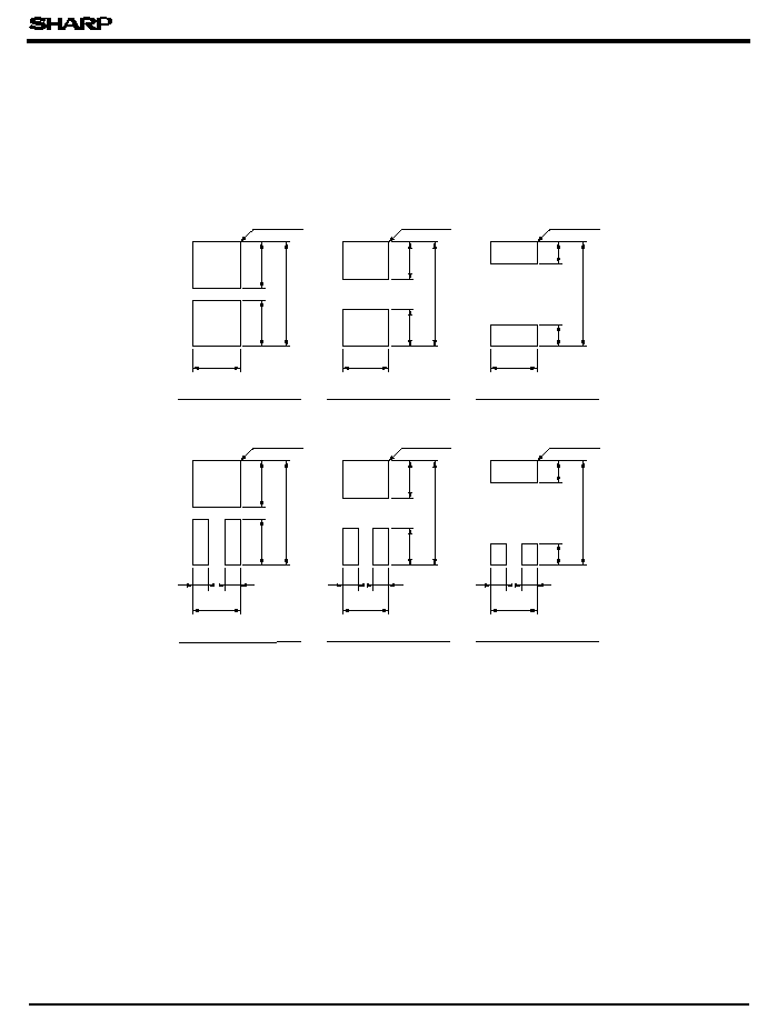
Recommended Mounting Hole Drawing
(Dimensions shown are recommended values.
Use the photointerrupters after checking the mounting strength and others on an actual machine.)
(Precautions for Operation)
1) In this product, the PWB is fixed with a hook, and cleaning solvent may remain inside the case;
therefore, dip cleaning or ultrasonic cleaning are prohibited.
2) Remove dust or stains, using an air blower or a soft cloth moistened in cleaning solvent.
However, do not perform the above cleaning using a soft cloth with solvent in the marking portion.
In this case, use only the following type of cleaning solvent for wiping off;
Ethyl alcohol, Methyl alcohol, Isopropyl alcohol
When the cleaning solvents except for specified materials are used, please contact us.
As for other general precautions, please refer to the chapter "Precautions for Use".
7.7
7.5
7.5
7.5
(Unit : mm)
17
8
-
R0.1
±
0.1
8
-
R0.1
±
0.1
Plate thickness : 1.6 mm
17
17
6
6
3.5
3.5
7.5
Plate thickness : 1.0 mm
Plate thickness : 1.2 mm
8
-
R0.1
±
0.1
General mounting type
7.7
7.5
7.5
7.5
17
Plate thickness : 1.6 mm
17
17
6
6
3.5
3.5
7.5
Plate thickness : 1.0 mm
Plate thickness : 1.2 mm
Reverse insertion
preventive type
12
-
R0.1
±
0.1
12
-
R0.1
±
0.1
12
-
R0.1
±
0.1
2.4
2.4
2.4
2.4
2.4
2.4
1. It is recommended to mount the photointerrupters on the shear droop surface (punch side) of the mounting plate (metal plate).
2. Mounting workability, shaking after mounting and mounting strength depend on the corner radius of the mounting plate and state of punching.
Determine the mounting hole dimensions after check on an actual machine.
3. General dimensional tolerances shall be ± 0.1 mm.
s
q