 | –≠–ª–µ–∫—Ç—Ä–æ–Ω–Ω—ã–π –∫–æ–º–ø–æ–Ω–µ–Ω—Ç: GP1UE28QK | –°–∫–∞—á–∞—Ç—å:  PDF PDF  ZIP ZIP |

GP1UE26RK/GP1UE27RK Series
GP1UE28RK/GP1UE28QK Series
GP1UE26RK/27RK/28RK/28QK Series
s
Outline Dimensions
5.6
2.2
2.9
4.3
4.7
7.6
8.6
±
0.5
*1
3.6
±
0.5
*3
2.9
*3
5.8
*3
2.9
5
3.6
0.4
1.7
1.7
5.85
7.55
1.4
1.4
2.2
0.5
1.4
1.4
2.54
2.54
Example of mounting drawing
from solder side (Reference)
*1
9.6
V
OUT
V
CC
GND
1
2
3
*1
2.54
*1
2.54
0.5
0.7
0.7
3
-
0.8
6.7
Center
of PD
1
2
3
1
2
3
1.*1 : Indicates root dimensions of connector.
2.Unspecified tolerance :
±
0.3
3.Case thickness : 0.3TYP
4.*2 : Exclude sagged solder
5.*3 : If there are difficulties to insert the GP1UE26RK series on PCB,
we recommend to expand
+
0.1mm from original 2.9mm.
5.6
2.2
1.25
1.25
2.9
4.3
4.7
7.6
13.8
±
0.5
*2
3.6
±
0.5
*3
2.9
*3
5.8
*3
2.9
10.2
3.6
0.4
1.7
1.7
5.85
7.55
1.4
1.4
2.2
0.5
1.4
1.4
2.54
2.54
Example of mounting drawing
from solder side (Reference)
*1
9.6
V
OUT
V
CC
GND
1
2
3
*1
2.54
*1
2.54
0.5
0.8
0.8
3
-
0.8
6.7
Center
of PD
1
2
3
3
2
1
1.*1 : Indicates root dimensions of connector.
2.Unspecified tolerance :
±
0.3
3.Case thickness : 0.3TYP
4.*2 : Exclude sagged solder
5.*3 : If there are difficulties to insert the GP1UE27RK series on PCB,
we recommend to expand
+
0.1mm from original 2.9mm.
GP1UE26RK Series
GP1UE27RK Series
Low Voltage Operation, Anti Electromagnetic
Induction Noise Type, Compact IR Detecting
Unit for Remote Control
1. AV equipments
2. Home appliances
s
Features
s
Applications
1. Low dissipation current:MAX.0.6mA (at V
CC
=
3V)
2. Low operating voltage:2.4 to 3.6V
3. Anti electromagnetic induction noise type.
4. Compact (case volume).
5. Various B.P.F. (Band Pass Frequency) frequency to meet different
user needs.
Notice
In the absence of confirmation by device specification sheets, SHARP takes no responsibility for any defects that may occur in equipment using any SHARP
devices shown in catalogs, data books, etc. Contact SHARP in order to obtain the latest device specification sheets before using any SHARP device.
Internet
Internet address for Electronic Components Group http://sharp-world.com/ecg/
(Unit : mm)
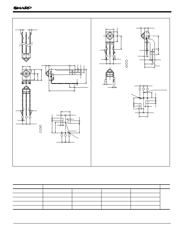
GP1UE26RK/27RK/28RK/28QK Series
GP1UE26RK
GP1UE260RK
GP1UE261RK
GP1UE262RK
GP1UE267RK
GP1UE27RK
GP1UE270RK
GP1UE271RK
GP1UE272RK
GP1UE277RK
GP1UE28RK
GP1UE280RK
GP1UE281RK
GP1UE282RK
GP1UE287RK
GP1UE28QK
GP1UE280QK
GP1UE281QK
GP1UE282QK
GP1UE287QK
Model No.
40
36
38
36.7
B.P.F. center frequency
56.8
Unit
kHz
s
Model Line-up
Diversified models with a different B.P.F. frequency are also available.
s
Outline Dimensions
5.6
2.2
1.25
1.25
2.9
4.3
4.7
7.6
17.8
±
0.5
*2
3.6
±
0.5
*3
2.9
*3
5.8
*3
2.9
14.2
3.6
0.4
1.7
1.7
5.85
7.55
6.7
1.4
1.4
2.2
0.5
1.4
1.4
2.54
2.54
Example of mounting drawing
from solder side (Reference)
*1
9.6
V
OUT
V
CC
GND
1
2
3
*1
2.54
*1
2.54
0.5
0.8
0.8
3
-
0.8
Center
of PD
1.*1 : Indicates root dimensions of connector.
2.Unspecified tolerance :
±
0.3
3.Case thickness : 0.3TYP
4.*2 : Exclude sagged solder
5.*3 : If there are difficulties to insert the GP1UE28RK series on PCB,
we recommend to expand
+
0.1mm from original 2.9mm.
1
2
3
1
2
3
2.54
Top of lenz
2.54
1.4
1.4
3.55
1.85
3.9
1.7
1.7
3
-
0.8
Example of mounting drawing
from solder side (Reference)
0.4
*1
1.7
*2
9.6
*3
2.9
*3
5.8
*3
2.9
3.7
1.4
1.4
5.4
6.8
2.2
2.75
5.6
2.9
4.3
3.6
9
.6
V
OUT
V
CC
GND
1
2
3
*1
2.54
*1
2.54
0.5
0.8
0.8
1.25
1.25
1
2
3
1
2
3
1.*1 : Indicates root dimensions of connector.
2.Unspecified tolerance :
±
0.3
3.Case thickness : 0.3TYP
4.*2 : Exclude sagged solder
5.*3 : If there are difficulties to insert the GP1UE28QK series on PCB,
we recommend to expand
+
0.1mm from original 2.9mm.
GP1UE28RK Series
GP1UE28QK Series
(Unit : mm)
GP1UE26RK/27RK/28RK/28QK Series
Parameter
Conditions
No input light
*3
I
OL
=
1.6mA
MIN.
-
V
CC
-
0.5
-
400
600
TYP.
0.4
-
-
-
-
MAX.
-
0.6
0.45
1 000
1 200
Unit
mA
V
V
µ
s
µ
s
Dissipation current
High level output voltage
Low level output voltage
High level pulse width
Symbol
I
CC
V
OH
T
1
V
OL
T
2
Low level pulse width
-
-
*4
-
kHz
f
0
B.P.F. center frequency
-
70
100
130
k
R
L
Output pull-up resistance
*3 The burst wave as shown in the following figure shall be transmitted by the transmitter shown in Fig. 1
The carrier frequency of the transmitter, however, shall be same as *4, and measurement shall be from just after starting the transmission until 50 pulse
*4 The B.P.F. center frequency f
0
varies with model, as shown in s
Model Line-up
(T
a
=
25∞C, V
CC
=+
3V)
s
Electro Characteristics
1 000
µ
s
600
µ
s
f
0
=(
*4
)
Duty 50%
Burst wave
s
Absolute Maximum Ratings
*1 No dew condensation is allowed
*2 For 5s (At mounting on PCB with thickness of 1.6mm)
Parameter
Symbol
Rating
Unit
Supply voltage
V
CC
V
Operating temperature
T
opr
-
10 to
+
70
∞
C
0 to
+
6.0
*1
*2
Storage temperature
T
stg
-
20 to
+
70
∞
C
Soldering temperature
T
sol
260
∞
C
(T
a
=
25
∞
C)
s
Recommended Operating Conditions
Parameter
Symbol Operating conditions
Unit
V
CC
2.4 to 3.6
V
Supply voltage
s
Internal Block Diagram
V
OUT
R
L
V
CC
GND
B.P.F.
Limiter
Demodulator Integrator Comparator

GP1UE26RK/27RK/28RK/28QK Series
Fig.2 Standard Optical System
Transmitter
Reception distance:L
Light detector face illuminance:E
V
(
indicates horizontal and vertical directions.)
V
OUT
Fig.1 Transmitter
20cm
10k
+
5V
10
µ
F
PD49PI
10k
V
OUT
Oscilloscope
Transmitter (GL521 used)
f
0
=
(
*
4)
Duty 50
%
In the above figure, the transmitter should be set so that the output V
OUT (P-P)
can be 40mV.
However, the
PD49PI
to be used here should be of the short-circuit current I
SC
=2.6
µ
A at E
V
=100 lx.
(E
V
is an illuminance by CIE standard light source A (tungsten lamp).)
s
Performance
Using the transmitter shown in Fig. 1, the output signal of the light detecting unit is good enough to meet the following items in the
standard optical system in Fig. 2.
1. Linear reception distance characteristics
When L=0.2 to 8.0(6.5)
*7
m,
*5
E
V
<
10 lx and
=
0∞ in Fig.2, the output signal shall meet the electrical characteristics in the attached
list.
2. Sensitivity angle reception distance characteristics
When L=0.2 to 6.0(4.5)
*7
m,
*5
E
V
<
10 lx and
30∞ in Fig.2, the output signal shall meet the electrical characteristics in the attached
list.
3. Anti outer peripheral light reception distance characteristics
When L=0.2 to 4.0(3.0)
*7
m,
*6
E
V
300 lx and
=
0∞ in Fig.2, the output signal shall meet the electrical characteristics in the attached
list.
*5 It refers to detector face illuminance
*6 Outer peripheral light source: CIE standard light source A shall be used and placed at 45∞ from perpendicular axis at the detector face center
*7 In case of B.P.F. center frequency: 56.8kHz model

GP1UE26RK/27RK/28RK/28QK Series
GND
(Circuit parameters)
R
1
=
47
±
5%
C
1
=
47
µ
F
C
O
+
V
e
V
O
GND
V
CC
V
OUT
R
1
In setting R
1
and C
1
, use suitable values after considering under the real condition
The circuit constant is a example. It is difference from mounting equipment. Please select it by your mounting equipment. This
device has a transistor as protection element between V
CC
and GND to improve anti-static electricity proof.
Please be carefully not to apply exceeding the absolute maximum ratings of applying voltage and continuous high voltage spike
noise because there is cases that transistor will be short by secondary breakdown generally.
In order to do difficultly, Please add CR filter (47
(1/10W), 10
µ
F or more) such as external circuit example above near V
CC
.
1. When this infrared remote control detecting unit shall be adopted for wireless remote control, please use it with the signal format of
transmitter, which total duty ratio D
t
(Emitting time
n
t
N
/ Transmitting time for 1 block T) is 40% or less. ON signal time T
ON
(Pulse width of the presence of modulated IR) should be 250(200:In case of B.P.F center frequency:56.8kHz model)
µ
s or more. In
case that the signal format of total duty and ON signal time is out of above conditions, there is a case that reception distance is
much reduced or output is not appeared.
2. Use the light emitting unit (remote control transmitter), in consideration of performance, characteristics, operating conditions of
light emitting device and the characteristics of the light detecting unit.
3. Pay attention to a malfunction of the light detecting unit when the surface is stained with dust and refuse.
Care must be taken not to touch the light detector surface.
If it should be dirty, wipe off such dust and refuse with soft cloth so as to prevent scratch. In case some solvents are required, use
methyl alcohol, ethyl alcohol or isopropyl alcohol only.
Also, protect the light detecting unit against flux and others, since their deposition on the unit inside causes reduction of the
function, fading of markings such as the part number.
4. The shield case should be grounded on PCB pattern.
(The area across the shield case and the GND terminal is internally conductive in some cases and non-conductive in some other
cases.)
5. Do not apply unnecessary force to the terminal and the case.
6. Do not push the light detector surface (photodiode) from outside.
7. To avoid the electrostatic breakdown of IC, handle the unit under the condition of grounding with human body, soldering iron, etc.
8. Do not use hole and groove set in the case of the light detecting unit for other purposes, since they are required to maintain the
specified performance.
9. External Circuit Examples (Mount the outer parts as near the unit as possible).
s
Precautions for Operation
N
=
1
t
1
t
2
t
3
t
n
T
ON
Transmitting time for 1 block:T
D
t
=(
t
N
/ T)
◊
100 (%)
n
N
=
1

GP1UE26RK/27RK/28RK/28QK Series
10. There is a possibility that noise on output may be caused by environmental condition (Disturbing light noise, Electromagnetic
noise, Power supply line noise, etc.) even if there is no input transmission signal.
11. Please shall confirm operation or your actual machine. Because the output pulse width of this product is fluctuated by
environmental conditions such as signal format, temperature, distance from transmitter, and so on.
12. In case that this product is kept in high humidity condition, it may be hard to solder, please be careful enough about storage
method.
Depend on the flux you select, there are different solderabilities, so please select a suitable flux and use it.
13. Please use this device away from the dew drop.
Be aware that the dew drop rusts shield case and others, may affect the electric characteristics.

NOTICE
G
The circuit application examples in this publication are provided to explain representative applications of SHARP
devices and are not intended to guarantee any circuit design or license any intellectual property rights. SHARP takes
no responsibility for any problems related to any intellectual property right of a third party resulting from the use of
SHARP's devices.
G
Contact SHARP in order to obtain the latest device specification sheets before using any SHARP device. SHARP
reserves the right to make changes in the specifications, characteristics, data, materials, structure, and other contents
described herein at any time without notice in order to improve design or reliability. Manufacturing locations are
also subject to change without notice.
G
Observe the following points when using any devices in this publication. SHARP takes no responsibility for damage
caused by improper use of the devices which does not meet the conditions and absolute maximum ratings to be used
specified in the relevant specification sheet nor meet the following conditions:
(i) The devices in this publication are designed for use in general electronic equipment designs such as:
- - - Personal computers
- - - Office automation equipment
- - - Telecommunication equipment [terminal]
- - - Test and measurement equipment
- - - Industrial control
- - - Audio visual equipment
- - - Consumer electronics
(ii) Measures such as fail-safe function and redundant design should be taken to ensure reliability and safety when
SHARP devices are used for or in connection with equipment that requires higher reliability such as:
- - - Transportation control and safety equipment (i.e., aircraft, trains, automobiles, etc.)
- - - Traffic signals
- - - Gas leakage sensor breakers
- - - Alarm equipment
- - - Various safety devices, etc.
(iii)SHARP devices shall not be used for or in connection with equipment that requires an extremely high level of
reliability and safety such as:
- - - Space applications
- - - Telecommunication equipment [trunk lines]
- - - Nuclear power control equipment
- - - Medical and other life support equipment (e.g., scuba).
G
If the SHARP devices listed in this publication fall within the scope of strategic products described in the Foreign
Exchange and Foreign Trade Law of Japan, it is necessary to obtain approval to export such SHARP devices.
G
This publication is the proprietary product of SHARP and is copyrighted, with all rights reserved. Under the copyright
laws, no part of this publication may be reproduced or transmitted in any form or by any means, electronic or
mechanical, for any purpose, in whole or in part, without the express written permission of SHARP. Express written
permission is also required before any use of this publication may be made by a third party.
G
Contact and consult with a SHARP representative if there are any questions about the contents of this publication.