 | –≠–ª–µ–∫—Ç—Ä–æ–Ω–Ω—ã–π –∫–æ–º–ø–æ–Ω–µ–Ω—Ç: GP2L26 | –°–∫–∞—á–∞—Ç—å:  PDF PDF  ZIP ZIP |

GP2L09/GP2L24/GP2L26
Subminiature, High Sensitivity
Photointerrupter
s
Outline Dimensions
(Unit : mm )
s
Features
s
Applications
1. Compact and thin
GP2L09
: Compact DIP, long lead type
2. Optimum detection distance: 0.6 to 0.8mm
3. High sensitivity
( I
C
: MIN. 0.5mA at I
F
= 4mA )
4. Visible light cut-off type
GP2L24
: Compact DIP type
GP2L26
: Flat lead type
1. Cassette tape recorders, VCRs
2. Floppy disk drives
3. Various microcomputerized control equip-
ment
C0.7
GP2L09
±
0.2
±
15
∞
1
1.75
2
0.8
4
3
±
15
∞
0.75
C0.7
1
1.7
1.75
2
4
GP2L24
3
±
0.2
0.75
C0.7
GP2L26
1.7
±
30
∞
±
20
∞
1
2
4
3
1
4
2
3
±
1.0
±
0.15
( 0.2
) Emitter center
(4.0)
( )
:
Reference dimensions
The dimensions indicated by
g
refer
to those measured from the lead base.
( )
:
Reference dimensions
The dimensions indicated by
g
refer
to those measured from the lead base.
( 0.2
) Emitter center
(4.0)
1 Anode
2 Emitter
3 Collector
4 Cathode
Internal connection diagram
(Common to 3 models )
( 0.2
) Emitter center
( )
:
Reference dimensions
1.75
4
-
(0.6)
GP2L09/GP2L24
GP2L26
( 0.4
) Detector center
Tolerance
:±
0.15mm
( 0.4
) Detector center
Tolerance
:±
0.15mm
( 0.4
) Detector center
Tolerance
:±
0.15mm
data books, etc. Contact SHARP in order to obtain the latest version of the device specification sheets before using any SHARP's device.
"
"
In the absence of confirmation by device specification sheets, SHARP takes no responsibility for any defects that occur in equipment using any of SHARP's devices, shown in catalogs,
:
0 to 20
∞
:
0 to 20
∞
g
4.0
0.2
1.7
0.15
12.5
1.0
g
4.0
0.2
4
-
0.5
+
0.2
-
0.1
4.0
+
0.2
-
0.1
3.0
+
0.2
-
0.1
4
-
0.2
+
0.3
-
0
4
-
0.4
+
0.2
-
0.1
4
-
0.15
+
0.2
-
0.1
4.0
+
0.2
-
0.1
3.0
+
0.2
-
0.1
3.5
+
1.0
-
0
4.0
+
0.2
-
0.1
0.4
+
0.2
-
0.1
0.15
+
0.2
-
0.1
3.0
+
0.2
-
0.1
13.0
±
1.0

GP2L09/GP2L24/GP2L26
s
Absolute Maximum Ratings
(Ta = 25∞C)
(Ta = 25∞C )
Parameter
Symbol
Rating
Unit
Input
Forward current
I
F
50
mA
Reverse voltage
V
R
6
V
P
75
Output
Collector-emitter voltage
V
CEO
35
V
Emitter-collector voltage
V
ECO
6
V
Collector current
I
C
50
mA
75
mW
Total power dissipation
P
tot
100
mW
Operating temperature
opr
- 25 to + 85
∞C
Storage temperature
T
stg
- 40 to + 100
∞C
T
sol
260
∞C
1
Soldering temperature
3 The condition and arrangement of the reflective object are shown in the right drawing.
4 Without reflective object
The ranking of collector current shall be
Power dissipation
P
C
mW
s
Electro-optical Characteristics
Parameter
Symbol
Conditions
MIN.
TYP.
MAX.
Unit
Input
Forward voltage
I
F
I
F
= 20mA
-
1.2
1.4
V
Reverse current
I
R
V
R
= 6V
-
-
10
µ
A
Output
Collector dark current
I
CEO
-
-
1x 10
- 6
A
Transfer-
charac-
teristics
3
Collector current
I
C
V
CE
= 2V, I
F
= 4mA
0.5
3.0
15.0
mA
Response time
Rise time
t
r
-
80
400
Fall time
t
f
-
70
400
4
Leak current
I
LEAK
I
F
= 4mA, V
CE
= 5V
-
-
5.0
V
CE
= 2V, I
C
= 10mA
R
L
µ
s
µ
s
µ
A
GP2L09, GP2L24
2.0mm
2.0mm
Soldering area
The hatched area more than 1mm
2
away from the lower edge of
package as shown in the drawing
below.
classified into the following 6 ranks.
1mm
2
1mm-thick glass
2 GP2L09
:
4mm
GP2L26
Soldering area
The hatched area more
than 2.0mm away from
the both edge of package
as shown in the drawing
below.
5
GP2L24
and
GP2L26
don't
(
GP2L09
,
GP2L24
,
GP2L26
)
Rank
Collector current I
C
( mA )
5
A
0.5 to 1.9
B
1.45 to 5.4
C
4.0 to 15.0
A or B
0.5 to 5.4
B or C
1.45 to 15.0
A, B or C
0.5 to 15.0
1 Within 5 seconds ( Soldering areas for each model are shown below. )
V
CE
T
Collector power dissipation
= 10V, I
F
= 0
= 100
, d = 1mm
Test Condition for Collector Current
Al evaporation
have A rank.

GP2L09/GP2L24/GP2L26
- 25
0
25
50
75 85
100
0
10
20
30
40
50
60
5
2
5
2
5
Duty ratio
Pulse width <=100
µ
s
2
0
0.5
1.0
1.5
2.0
2.5
3.0
1
2
5
10
20
50
100
200
500
25∞C
0∞C
- 25∞C
50∞C
0
25
- 25
0
20
40
60
120
Power dissipation P
(
mW
)
50
100
75
80
100
85
75
2.5
5.0
7.5
10.0
12.5
0
0
5
10
15
20
25
15.0
2
4
6
8
10
0
0
2
4
6
8
10
12
14
16
12
4mA
2mA
7mA
10mA
Fig. 6 Collector Current vs.
Collector-emitter Voltage
Fig. 1 Forward Current vs.
Ambient Temperature
Forward current I
F
(
mA
)
Ambient temperature T
a
(∞C)
Ambient temperature T
a
(∞C)
Peak forward current I
FM
(
mA
)
Forward voltage V
F
(V)
Forward current I
F
(
mA
)
T
a
= 25∞C
P
tot
P, P
C
T
a
= 75∞C
V
CE
= 2V
T
a
= 25∞C
Collector current I
C
(
mA
)
Forward current I
F
( mA )
Collector-emitter voltage V
CE
(V)
Collector current I
C
(
mA
)
I
F
= 15mA
P
c
( MAX. )
T
a
= 25∞C
Fig. 2 Power Dissipation vs.
Ambient Temperature
Fig. 3 Peak Forward Current vs.
Duty Ratio
Fig. 4 Forward Current vs.
Forward Voltage
Fig. 5 Collector Current vs.
Forward Current
10
- 3
10
- 2
10
- 1
2000
1000
500
200
100
50
20
1

GP2L09/GP2L24/GP2L26
0
25
- 25
0
25
50
75
150
50
100
75
100
125
- 25
0
10
- 11
25
100
50
75
5
10
- 10
5
10
- 9
5
10
- 8
5
10
- 7
5
10
- 6
5
10
- 5
5
10
- 4
10
20
50
100
200
500
1000
1
10
100
1000
1000
Output
Output
Input
0
1
2
4
5
40
60
20
0
3
Relative collector current
(
%
)
Ambient temperature T
a
(∞C)
Fig. 8 Collector Dark Current vs.
Ambient Temperature
V
CE
= 10V
Collector dark current I
CEO
(
A
)
Ambient temperature T
a
(∞C)
I
F
= 4mA
V
CE
= 5V
V
CE
= 2V
T
a
= 25∞C
t
d
t
s
V
CE
= 2V
I
C
= 10mA
T
a
= 25∞C
t
r
t
f
t
d
t
s
Response time
(
µ
s
)
Relative collector current
(
%
)
d ( mm)
V
CC
Input R
D
R
L
t
d
t
r
t
s
t
f
90
%
10
%
Response time
(
µ
s
)
Distance between Sensor and
Al Evaporation Glass
I
F
= 4mA
V
CE
= 2V
T
a
= 25∞C
I
C
= 10mA
1000
500
200
100
50
20
10
5
2
1
1000
500
200
100
50
20
10
5
2
1
0.5
0.2
0.1
Fig. 7 Relative Collector Current vs.
Ambient Temperature
t
r
t
f
Fig. 9-a Response Time vs.
Test Circuit for Response Time
Fig.10 Relative Collector Current vs.
80
100
Distance between sensor and Al evaporation glass
Fig. 9-b Response Time vs.
(GP2L09)
(GP2L24/GP2L26)
Load Resistance
Load resistance R
L
(
)
Load resistance R
L
(
)
Load Resistance
GP2L09/GP2L24/GP2L26
0
2
4
40
60
20
0
6
d= 1mm
- 1
1
3
5
10
Frequency f ( Hz )
0
- 5
- 10
- 15
- 20
2
5
2
5
2
5
600
700
800
900
1000
1200
80
100
40
60
20
0
1100
Correspond to Fig.10
Al evaporation
d
Correspond to Fig.11
OMS card
L
=
0
d
+
White
Lmm
Test condition
d
=
1mm
-
-
d
=
1mm
Test condition
Lmm
White
+
d
L
=
0
OMS card
Correspond to Fig.12
Black
Black
- 20
- 15
- 10
- 5
0
Frequency f ( kHz )
100
7
5
3
1
- 1
d= 1mm
6
0
20
60
40
100
80
4
2
0
- 2
GP2L24
2
100
5
10
I
F
= 4mA
V
CE
= 2V
T
a
= 25∞C
Relative collector current
(
%
)
Card moving distance L ( mm )
Card Moving Distance (1)
Card Moving Distance (2)
I
F
= 4mA
V
CE
= 2V
T
a
= 25∞C
Relative collector current
(
%
)
Card moving distance L ( mm )
(EX.: GP2L24)
I
F
V
CE
=
2V
I
F
=
4mA
V
CE
=
2V
GP2L09)
R
L
= 1k
/
)
I
F
= 10mA
V
CE
= 2V
T
a
= 25∞C
R
L
= 1k
Relative sensitivity
(
%
)
Wavelength
( nm )
Position Characteristics
10
2
10
3
10
4
10
5
V
CE
= 2V
I
C
= 10mA
T
a
= 25∞C
T
a
= 25∞C
80
100
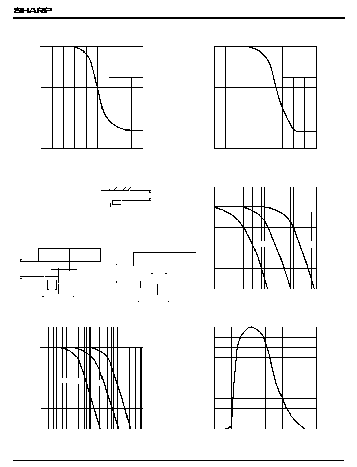
Fig.12 Relative Collector Current vs.
Fig.13 Frequency Response (
=
4mA
Test Condition for Distance & Detecting
Fig.14 Frequency Response (GP2L24 GP2L26
Fig.15 Spectral Sensitivity (Detecting Side)
Fig.11 Relative Collector Current vs.
10
2
10
3
10
4
10
5
10
6
Voltage gain Av
(
dB
)
Voltage gain Av
(
dB
)

GP2L09/GP2L24/GP2L26
s
Precautions for Use
Ethyl alcohol, Methyl alcohol, Isopropyl alcohol, Freon TE, Freon TF, Diflon solvent S3-E
When the cleaning solvents except for specified materials are used, please consult us.
( 3) Remove dust or stains, using an air blower or a soft cloth moistened in cleaning solvent.
However, do not perform the above cleaning using a soft cloth with cleaning solvent in the
marking portion.
In this case, use only the following type of cleaning solvent used for wiping off:
( 1) In order to stabilize power supply line, connect a by-pass capacitor of more than 0.01
µ
F bet-
ween Vcc and GND near the device.
( 2) In this product, the PWB is fixed with a resin cover, and cleaning solvent may remain inside
the case; therefore, dip cleaning or ultrasonic cleaning are prohibited.
( 4) As for other general cautions, refer to the chapter " Precautions for Use " .