GP2TC2
GP2TC2
s
Absolute Maximum Ratings
s
Recommend Operating Conditions
s
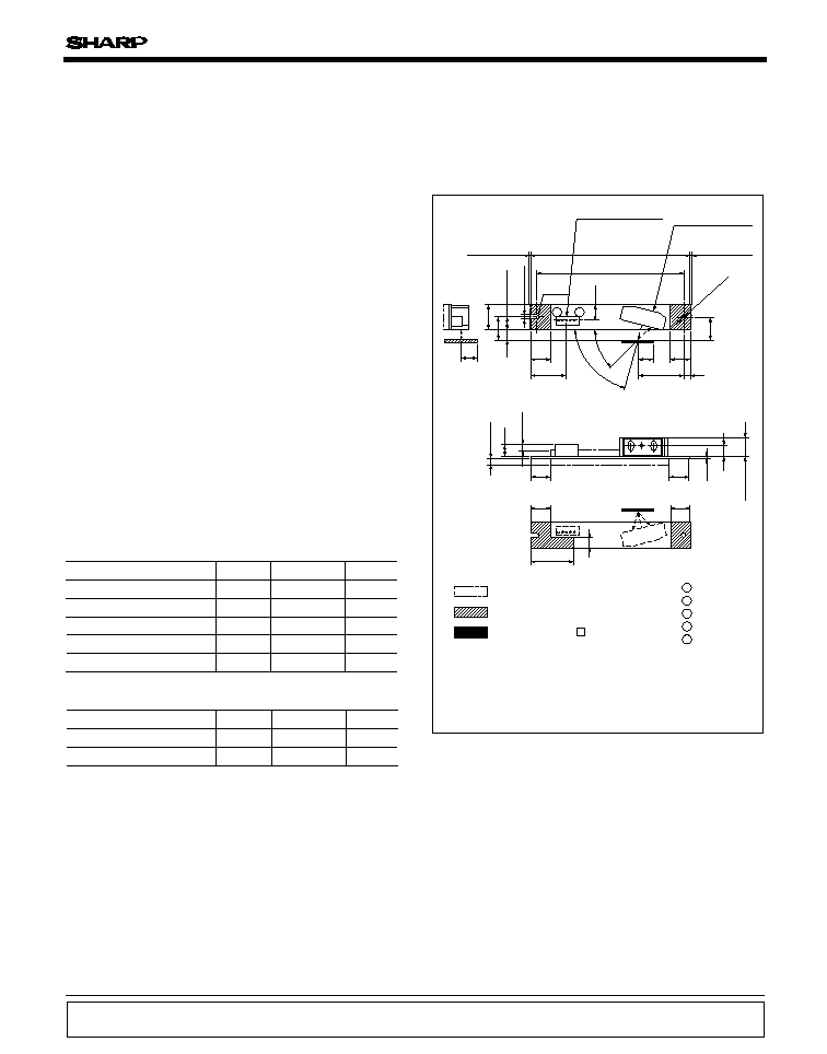
Outline Dimensions
(Unit : mm)
Color Toner Density (Adhesive
Volume) Sensor by Diffusive/
Mirror Reflection Method
1. Full-color copiers
2. Color LBPs
s
Features
s
Applications
1. Adopted diffusive reflection and mirror reflection method
Color toner detection : diffusive reflection method
Black toner detection : mirror reflection method
2. Analog output according to amount of reflective light
(adhesive volume of toner)
3. 2 system output : adhesive volume of black toner
adhesive volume of color toner
4. Detection range of toner density
(Y, M, C : 0 to 1.0mg/cm
2
)
(K : 0 to 0.6mg/cm
2
)
5. High resolution (0.1mg/cm
2
)
6. Output can be adjusted by control of LED current
Parameter
Symbol
Rating
Unit
V
CC
-
0.3 to 7
V
I
F
50
mA
�
C
V
O
-
0.3 to Vcc
+
0.3
-
20 to
+
70
V
T
stg
Operating voltage
LED current
Output terminal voltage
T
opr
0 to
+
60
�
C
Operating termperature
Storage temperature
(Ta
=
25
�
C, Vcc
=
5V)
Reflective object( 16mm)
Burr 0.6
MAX.
Burr 0.6
MAX.
8
80
10
23
3
10
10
10
22
L
7.5
Center of reflective object
(45
�
)
(75
�
)
2-6.25
L
(5)
12.5
10
18
8
5
10
3.0
+
0.1
-
0
9.5
MAX.
3
MAX.
3.5
MAX.
(6)
0.8
5
73
�
0.5
0.3
+
0.1
-
0
5
1
R1.5
Optical sensor
Device mount area
PCB pattern prohibited area
1
2
3
4
5
V
CC
GND
V
O
2
V
O
1
LED
g
( ) : Reference dimensions
g
Unspecified tolerance :
�
0.3mm
g
Size L in the diagram is referred to recommended service
conditions.
g
Sensor optical portion clearance : 0.3mm MAX.
Connector
Made by MOLEX
53324-0510
Notice
In the absence of confirmation by device specification sheets, SHARP takes no responsibility for any defects that may occur in equipment using any SHARP
devices shown in catalogs, data books, etc. Contact SHARP in order to obtain the latest device specification sheets before using any SHARP device.
Internet
Internet address for Electronic Components Group http://www.sharp.co.jp/ecg/
Parameter
Symbol
Rating
Unit
V
CC
4.5 to 5.5
V
L
11.0 to 11.5
mm
Supply voltage
Detection distance range
GP2TC2
s
Electro-optical Characteristics
Parameter
Symbol
Conditions
MIN.
TYP.
MAX.
Unit
Output voltage
Displacement of output voltage
Displacement of output voltage
V
O
1
A
0.73
1.17
V
V
V
V
V
V
V
V
-
-
�
s
�
s
mA
Rise time
V
O
1
BA
V
O
2
A
V
O
2
C0
V
O
1
0
V
O
1
A0
V
O
2
0
V
O
2
A0
V
O
1
2
V
O
2
2
tf
tr
I
CC
1.61
2.12
2.81
3.50
0.2
0.6
1.0
0.1
0.7
1.3
1.56
1.74
1.92
0.39
0.45
0.51
0.53
0.57
0.61
2.02
2.11
2.20
3.75
4.05
4.35
0.19
0.21
0.23
-
70
300
-
70
300
-
4
12
Consumption current
Fall time
(Ta
=
25
�
C, V
CC
=
5V)
Reflective object A
(V
O
1
A
:I
FM
=
15mA, V
O
2
A
:I
FM
=
20mA)
LED current I
FM
=
0mA
V
O
1
A
-
V
O
1
0
V
O
2
A
-
V
O
2
0
Consumption current at LED current I
FM
=0mA
Displacement of output voltage V
O
1 when
reflective object is changed from A to B (I
FM
=
15mA)
V
O
2
C0
=
V
O
2
C
-
V
O
2
0
(V
O
2
C
:Reflective object C, I
FM
=
20mA)
V
O
1
2
=
(
V
O
1
BA
+
V
O
1
A0
) /
V
O
1
A0
,
V
O
2
2
=
V
O
2
C0
/
V
O
2
A0
Reflective object C (Munsell N2 no gloss(Reflectivity 3.1%))
(V
O
1
A
: I
FM
=15mA, V
O
2
A
: I
FM
=20mA)
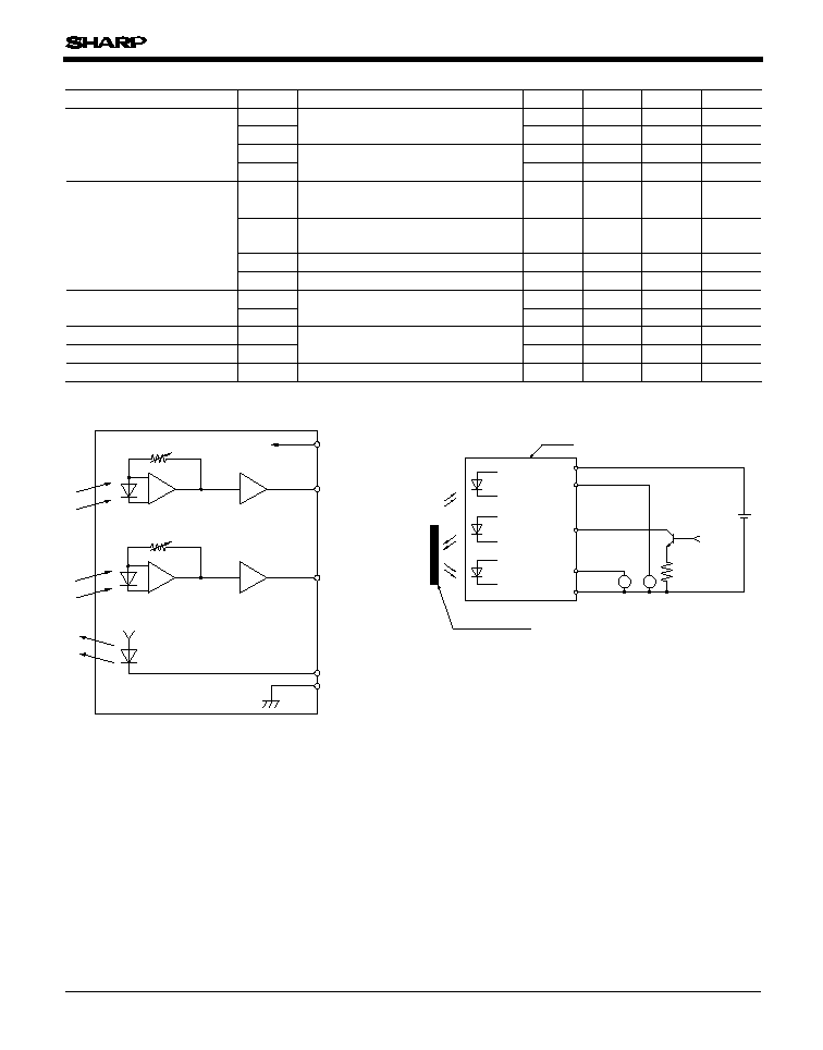
Fig.1 Internal Block Diagram
Fig.2 Schematic measurement block
diagram
I/V converter1
AMP1
V
CC
(5V)
V
O
1(Y,M,C)
V
O
2(K)
GND
LED
AMP2
V
CC
Infrared emitting diode
PD1
VR1
I/V converter2
PD2
VR2
V
V
5V
V
CC
V
O1
LED
V
O2
GND
PD1
LED
PD2
Reflective object
Sensor

GP2TC2
Fig.5 Measurement Condition
8
1
1
.
2
5
23
5
1
Reflective object A, B, C
Reflective object A : Munsell N4.5
no gloss (reflectivity 15.6%)
Reflective object B : Munsell N7.75 no gloss (reflectivity 54.8%)
Reflective object C : Munsell N2
no gloss (reflectivity 3.1%)
Fig.3 LED lighting condition
ON
OFF
t
=
2ms
I
FM
t
=
10ms
Fig.4 Response Time
Input
(LED current)
90%
10%
Output
(V
O
1,V
O
2)
t
r
t
f
s
Example of application
1. Apply V
CC
=
5V and measure V
O
1
0
at V
O
1, V
O
2
0
at V
O
2.
2. In order to stabilize output voltage measure 3. to 5. on the LED lighting condition shown in Fig.3 for example.
3. Measure the output voltage V
O
1 and V
O
2 and adjust I
FM
in order to fix
V
O
1 and
V
O
2
1
(determine value by your actual
application). After the adjustment, memorize the values, V
O
1, V
O
2 and I
FM
, (Adjust I
FM
for V
O
1 and V
O
2 each, and memorize them.)
(If there are the initial memorized values, V
O
1, V
O
2 and I
FM
, measure V
O
1 and V
O
2 at memorized I
FM
. If there are difference
between the measured values and memorized values adjust I
FM
to let V
O
1 and V
O
2 be initial values.)
4. Attach the color toner and measure the output voltage at V
O
1 (I
FM
at the value memorized at 3.). Determine the ouput voltage
difference
V
O
1 between the measured value and memorized value V
O
1 at 3, and adjust the attached color toner amount.
5. Attach the black toner and measure the output voltage at V
O
2 (I
FM
at the value memorized at 3.). Determine the ouput voltage
difference
V
O
2 between the measured value and memorized value V
O
2 at 3, and adjust the attached black toner amount.
6. After the measurement, set I
FM
=
0mA and turn off the LED.
7. To measure them again, start from 1.
Note V
O
1
0
: Output voltage at I
FM
=
0mA
V
O
2
0
: Output voltage at I
FM
=
0mA
V
O
1 : V
O
1 terminal ouput voltage at no toner
V
O
2 : V
O
2 terminal ouput voltage at no toner
V
O
1
1
: V
O
1
-
V
O
1
0
V
O
2
1
: V
O
2
-
V
O
2
0
V
O
1
: Output voltage when black toner is attached
-
V
O
1
V
O
2
: Output voltage when black toner is attached
-
V
O
2
I
FM
: LED current
GP2TC2
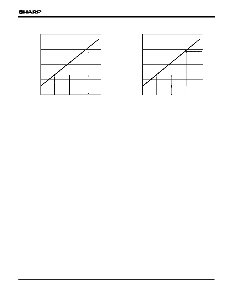
Fig.6 Output Voltage vs. Reflectivity of
Reflective Objects
Fig.7 Output Voltage vs. Reflectivity of
Reflective Objects
O
u
t
p
u
t
v
o
l
t
a
g
e
V
O
1
(
V
)
0
4.0
3.0
2.0
1.0
A
B
Reflectivity of reflective object (%)
V
O
1
0
V
O
1
A0
V
O
1
BA
V
O
1
A
V
O
1
O
u
t
p
u
t
v
o
l
t
a
g
e
V
O
2
(
V
)
0
4.0
3.0
2.0
1.0
C
A
Reflectivity of reflective object (%)
V
O
2
0
V
O
2
C0
V
O
2
AO
V
O
2
V
O
2
A

115
Application Circuits
NOTICE
qThe circuit application examples in this publication are provided to explain representative applications of
SHARP devices and are not intended to guarantee any circuit design or license any intellectual property
rights. SHARP takes no responsibility for any problems related to any intellectual property right of a
third party resulting from the use of SHARP's devices.
qContact SHARP in order to obtain the latest device specification sheets before using any SHARP device.
SHARP reserves the right to make changes in the specifications, characteristics, data, materials,
structure, and other contents described herein at any time without notice in order to improve design or
reliability. Manufacturing locations are also subject to change without notice.
qObserve the following points when using any devices in this publication. SHARP takes no responsibility
for damage caused by improper use of the devices which does not meet the conditions and absolute
maximum ratings to be used specified in the relevant specification sheet nor meet the following
conditions:
(i) The devices in this publication are designed for use in general electronic equipment designs such as:
--- Personal computers
--- Office automation equipment
--- Telecommunication equipment [terminal]
--- Test and measurement equipment
--- Industrial control
--- Audio visual equipment
--- Consumer electronics
(ii)Measures such as fail-safe function and redundant design should be taken to ensure reliability and
safety when SHARP devices are used for or in connection with equipment that requires higher
reliability such as:
--- Transportation control and safety equipment (i.e., aircraft, trains, automobiles, etc.)
--- Traffic signals
--- Gas leakage sensor breakers
--- Alarm equipment
--- Various safety devices, etc.
(iii)SHARP devices shall not be used for or in connection with equipment that requires an extremely
high level of reliability and safety such as:
--- Space applications
--- Telecommunication equipment [trunk lines]
--- Nuclear power control equipment
--- Medical and other life support equipment (e.g., scuba).
qContact a SHARP representative in advance when intending to use SHARP devices for any "specific"
applications other than those recommended by SHARP or when it is unclear which category mentioned
above controls the intended use.
qIf the SHARP devices listed in this publication fall within the scope of strategic products described in the
Foreign Exchange and Foreign Trade Control Law of Japan, it is necessary to obtain approval to export
such SHARP devices.
qThis publication is the proprietary product of SHARP and is copyrighted, with all rights reserved. Under
the copyright laws, no part of this publication may be reproduced or transmitted in any form or by any
means, electronic or mechanical, for any purpose, in whole or in part, without the express written
permission of SHARP. Express written permission is also required before any use of this publication
may be made by a third party.
qContact and consult with a SHARP representative if there are any questions about the contents of this
publication.