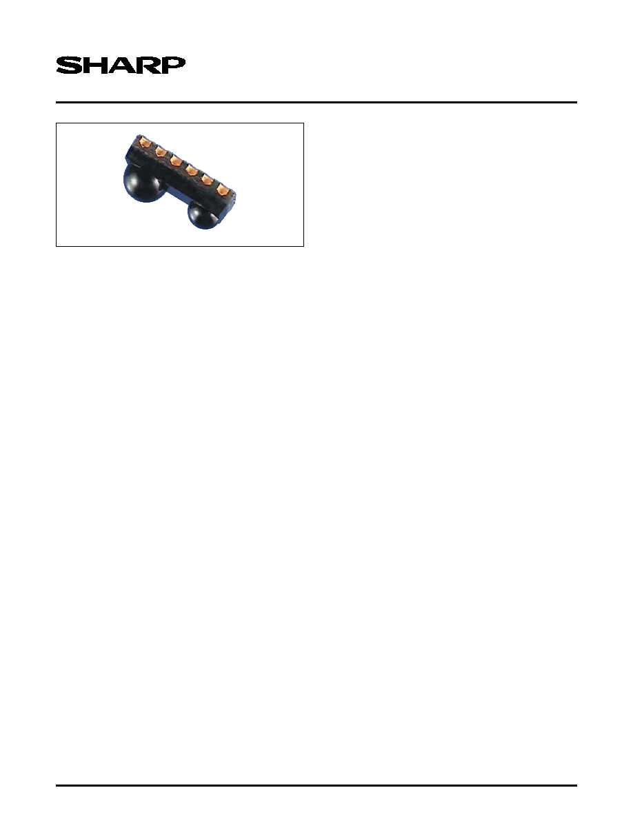
Technical Information
1
GP2W0001YP/GP2W0002YP
IrDA Technical Information
Low Power Infrared Transceiver
FEATURES
∑ IrDA 115 kbit/s Low Power Option Compatible:
≠ I
F
= 27 mA (TYP.) for an operating distance of
20 cm
∑ Small Package Design for IrDA 115 kbit/s 1 meter
Compliant Infrared Transceiver 8.7 (W) ◊ 4.2 (D) ◊
3.15 (H) mm
∑ Fits within Mobile Phone Connector Dimensions
∑ Low Power Consumption and Built-in Shut-Down
Mode (1
µA MAX.)
∑ Wide Range of Operating Voltages provides power
supply design flexibility (V
CC
= 2.7 V to 5.5 V)
∑ Solder Reflow Compatibility for automated produc-
tion processes
∑ SMD Package allows both Vertical and Horizontal
mounting on PCBs Description
DESCRIPTION
The SHARP GP2W0001YP is a standard trans-
ceiver module. Even at low operating voltages, it pro-
vides a reliable interface between logic and IR signals
for through-air, serial, half-duplex IR wireless data
links and is designed to satisfy IrDA physical layer
specifications.
The GP2W0002YP is the same module, and adds an
integral Electro-Magnetic Interference (EMI) shield.
While IR energy is inherently immune to EMI, the receiv-
ing devices themselves are not. This shield provides an
additional level of protection in electromagnetically noisy
environments such as PCs and other digital products.
The SHARP GP2W0001YP/GP2W0002YP infrared
transceiver modules contain a high speed, high effi-
ciency, low power consumption AlGaAs LED, silicon PIN
photodiode, and a low power bipolar integrated circuit.
The IC contains an LED driver circuit and a receiver, pro-
viding the Rx output. IrDA data rates of 2.4 kbit/s to
115.2 kbit/s are supported at both 20 cm and one-meter
distances. At the one-meter range, emitter current is
approximately I
F
= 300 mA and in the IrDA Low Power
Option communication mode I
F
= 27 mA. This dual
mode communication capability provides wider product
applications, such as a wireless data link with PCs,
PDAs, or any other IrDA compliant application already
on the market.
The GP2W0001YP/GP2W0002YP transceiver
modules may be operated over a power supply range
of 2.7 V to 5.5 V without any performance degradation.
This provides a single part with a wide variety of
design applications.
For power-conscious applications, the transceiver
module has a built-in Shutdown mode. This reduces
the receiver's current consumption to 1
µA (MAX.) dur-
ing Shutdown. The transmitter and receiver circuits are
separate, allowing the transmitter LED to be driven
when in Shutdown mode.
OUTLINE DIMENSIONS
The dimensions shown in Figure 1 and Figure 2 are
only for design reference, and are subject to change
without notice. The metal shield case version
GP2W0002YP, (for excellent noise immunity) is shown
in Figure 2. Contact your local SHARP office for the lat-
est device specifications.
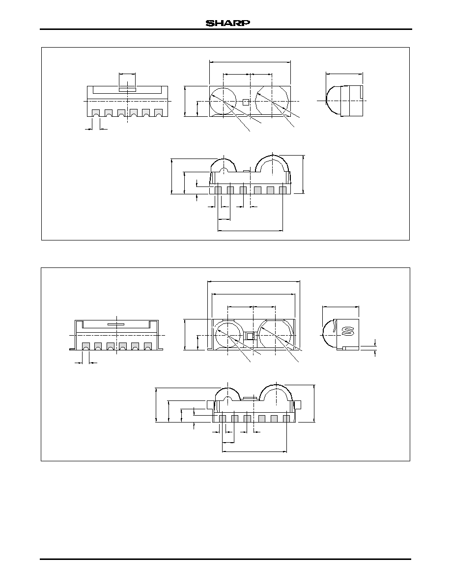
GP2W0001YP/GP2W0002YP
Low Power Infrared Transceiver
2
Technical Information
Figure 1. GP2W0001YP Outline Dimensions
Figure 2. GP2W0002YP (with Shielding Case) Outline Dimensions
1.1
TRANSMITTER
CENTER
RECEIVER
CENTER
2.8
3.6
2.0
1.7
4.2
2.2
3.5
0.8
0.8
0.7
1.4
7.0
2.95
4.2
8.7
2.325
3.15
NOTES:
1. Dimensions are in mm.
2. Unspecified tolerances are ±0.3 mm.
3. Resin burrs are not included in this
outline dimension drawing.
4. Package material: Visible light
cut-off resin (Color: black)
5. Weight: Approximately 0.12 g
6. Pin assignment: See Figure 5 and Table 1.
GP2W0001YP-20
1.1
10.2
4.2
1.7
3.4
3.5
4.2
2.2
1.55
0.8
0.7
9.2
2.95
0.8
1.4
0.7
7.0
2.325
RECEIVER
CENTER
3.6
TRANSMITTER
CENTER
2.8
GP2W0001YP-21
NOTES:
1. Dimensions are in mm.
2. Unspecified tolerances are ±0.3 mm.
3. Resin burrs are not included in this
outline dimension drawing.
4. Package material: Visible light
cut-off resin (Color: black)
5. Weight: Approximately 0.12 g
6. Pin assignment: See Figure 5 and Table 1.

Low Power Infrared Transceiver
GP2W0001YP/GP2W0002YP
Technical Information
3
Solder Paste Footprints
Figure 3 and Figure 4 are the Solder Paste footprint
drawings for both parts. Note that the GP2W0002YP
footprint in Figure 4 is compatible with both parts.
Figure 3. GP2W0001YP Soldering Footprint
Figure 4. GP2W0002YP Soldering Footprint
0.9
1.7
0.7
P 1.4 ◊ 5 = 7
NOTE: Viewed from the parts side of PCB.
LENS (PD/LED) SIDE
GP2W0001YP-22
1
2
3
4
5
6
0.9
0.8
0.8
LENS (PD/LED) SIDE
1.7
1.05
2.025
0.7
P 1.4 ◊ 5 = 7
10
GP2W0001YP-23
1
2
3
4
5
6
NOTE: Viewed from the parts side of PCB.
Table 1. Pinouts
PIN NO.
DESCRIPTION
SYMBOL
1
LED Anode
LEDA
2
Transmitter Data Input
TxD
3
Shut Down Circuit Input
SD
4
Receiver Data Output
RxD
5
Ground
GND
6
Supply Voltage
V
CC
Figure 5. Pin Locations
GP2W0001YP-28
PIN 1
PIN 6
PIN 1
PIN 6

GP2W0001YP/GP2W0002YP
Low Power Infrared Transceiver
4
Technical Information
ABSOLUTE MAXIMUM RATINGS
NOTES:
1. An in-band optical signal is a pulse/sequence where the peak
wavelength,
p, is defined as 850 nm < p < 900 nm, and the
pulse characteristics are compliant with the IrDA Physical Layer
2. See `IrDA Physical Layer Link Specification, Appendix A' for
ambient light conditions.
3. See Figure 6.
RECOMMENDED OPERATING CONDITIONS
NOTES:
1. Measured at the input circuit, not the device pin. Tx input should
not exceed 0.8 V
CC.
2. 0.4 or Open
PARAMETER
SYMBOL
MIN.
MAX.
UNIT
CONDITIONS
NOTES
Supply Voltage
V
CC
0
6.0
V
Peak Forward LED Current
I
FM
500
mA
Pulse 78.1 ms, 3/16-duty cycle
1, 2, 3
Operating Temperature
T
OPR
-10
+70
∞C
3
Soldering Temperature
T
SOL
230
∞C
Solder reflow time: 5 seconds
Storage Temperature
T
STG
-20
+85
∞C
PARAMETER
SYMBOL
MIN.
MAX.
UNIT
NOTES
Supply Voltage
V
CC
2.7
5.5
V
Logic High Transmitter Input Voltage (TxIN)
V
IHTXD
2.4
V
CC
V
1
Logic Low Transmitter Input Voltage (TxIN)
V
ILTXD
0.4
V
Shutdown Circuit High Level Input Voltage
V
IHSD
V
CC
≠ 0.6
V
CC
V
Shutdown Circuit Low Level Input Voltage
V
ILSD
0.0
0.4
V
2
Data Rate
BR
2.4
115.2
kbit/s
Operating Temperature
T
OPR
-10
70
∞C
Figure 6. Peak Forward Current vs. Temperature
GP2W0001YP-27
PEAK
FORWARD
CURRENT
I
FM
(mA)
300
400
200
100
-10
60 70
100
75
50
25
AMBIENT TEMPERATURE T
A
(
∞C)
0
0

Low Power Infrared Transceiver
GP2W0001YP/GP2W0002YP
Technical Information
5
ELECTRICAL AND OPTICAL SPECIFICATIONS
NOTES:
1. These specifications reflect the Recommended Operating Condi-
tions, unless otherwise noted.
2. All typical values are at 25∞C and 3.3 V, ambient light on the
receiver surface under 10 Lux, unless otherwise noted.
3. See Figure 7, Figure 8, and Figure 9
PARAMETER
SYMBOL
MIN.
TYP. MAX.
UNIT
CONDITIONS
NOTES
Supply Voltage
V
CC
2.7
5.5
V
Maximum Reception
Distance
L1
0.2
m
2
1/2
15∞, I
E
= 3.6 mW/sr
L2
1.0
m
2
1/2
15∞, I
E
= 40 mW/sr
Data Rate
BR
2.4
115.2
kbit/s
Operating Temperature
T
OPR
-10
70
∞C
RECEIVER
High Level Output Voltage
V
OH
4.5
V
V
CC
= 5 V
V
OH
2.5
V
V
CC
= 3 V
Low Level Output Voltage
V
OL1
0.6
V
V
CC
= 5 V, I
OL
= 400 mA RxD = ON
3
V
OL2
0.6
V
V
CC
= 3 V, I
OL
= 400 mA RxD = ON
3
Viewing Angle
2
30
degrees
Low Level Pulse Width
t
W1
0.8
16
µs
BR = 2.4
kbit/s
(pulse width 78.12
µs)
t
W2
0.8
8
µs
BR = 115.2
kbit/s
(pulse width 1.63
µs)
I
CC1
1.0
1.4
mA
No input signal, V
CC
= 5.0 V, output open,
V
IHSD
= V
CC
- 0.6 V
Current Consumption
0.7
1.0
mA
No input signal, V
CC
= 3.0 V, output open,
V
IHSD
= V
CC
- 0.6 V
I
CC2
1.0
µA
Shut-down Mode
Rise Time
t
R
1.2
µs
3
Fall Time
t
F
0.2
µs
3
TRANSMITTER
Radiant Intensity
I
E1
3.6
28.8
mW/sr
I
F
= 27 mA, 2
1/2
15∞
I
E2
40
350
mW/sr
I
F
= 300 mA, 2
1/2
15∞
Peak Emission Wavelength
p
850
870
900
nm
I
F
= 20 mA
Peak LED Current
I
LEDA
500
mA
All modes, PW = 78.1
µs or less,
3/16 duty cycle
High Level Input Voltage
V
IH
2.4
V
CC
V
Measured at input circuit. Device pin will
usually not exceed 0.8 V
Low Level Input Voltage
V
IL
0.0
0.4
V
Figure 7. Detector Input Signal Waveform
NOTE: At BR = 2.4 kbit/s: t
1
= 416.7 µs, t
2
= 78.1 µs
At BR = 115.2 kbit/s: t
1
= 8.68 µs, t
2
= 1.63 µs
t
1
t
2
RADIATION
INTENSITY OF
TRANSMITTER
3.6 mW/sr MIN.
GP2W0001YP-24