IrDA Technical Information
1
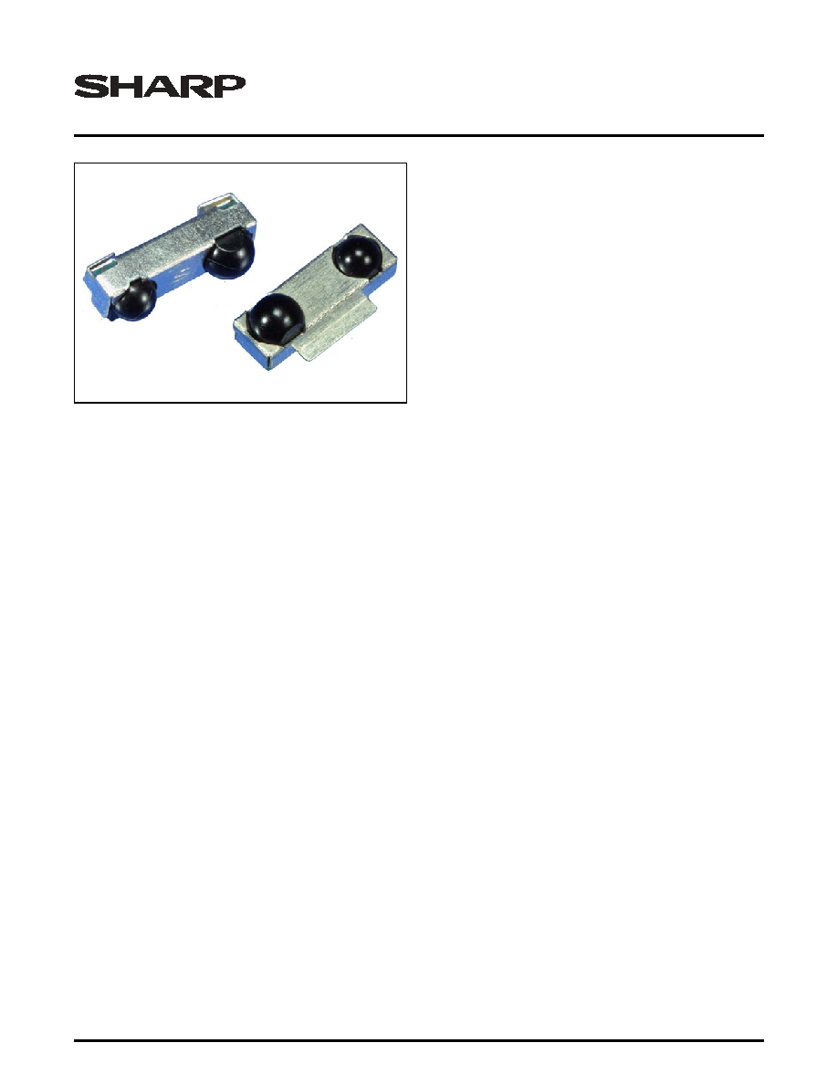
GP2W0004YP/XP
IrDA Technical Information
Infrared Transceiver
FEATURES
∑ IrDA 115 kbit/s, 1 meter Transceiver
∑ Small Package Design
≠ W 9.21 ◊ D 3.86 ◊ H 2.71 mm
∑ Receiver Output Provides a Gated Output Pulse for
the Received Input Signal
∑ Fits Within Mobile Phone Connector Dimensions
∑ Low Power Consumption and Built-in Shut-Down
Mode (1
µ
A MAX.)
∑ Wide Range Operating Voltage
≠ VCC = 2.4 V - 5.5 V
∑ Wide Operating Temperature Range
≠ -20∞C to +85∞C
∑ Split Voltage Design
≠ LED Voltage Separate from Operating Voltage
∑ Internal Echo-Cancel Function
≠ RX Data Output Disabled when the Transmit LED
is Active
∑ LED Disabled During Shutdown Mode
∑ Solder Reflow Capability for Automated Production
Process
∑ GP2W0004YP is Electrically and Mechanically
Compatible with IRMS5000, HSDL-3000, CHX1010,
MiniSIR2-1
∑ Top View Version: GP2W0004XP
DESCRIPTION
The SHARP GP2W0004YP has a wide operating
voltage range and is one of the smallest IrDA one-
meter transceiver modules. It provides the interface
between logic and IR signals for through-air, serial,
half-duplex IR wireless data links and is designed to
satisfy the IrDA physical layer specifications.
This part features an integral Electro-Magnetic Inter-
ference (EMI) shield. IR energy is inherently immune to
EMI; however, the receiving devices are sensitive to
EMI. The shield provides additional protection in noisy
environments such as PCs and other digital products.
The SHARP GP2W0004YP infrared transceiver
module contains a high speed, high efficiency, low
power consumption AlGaAs LED, silicon PIN photo-
diode, and low power bipolar integrated circuit. The IC
contains an LED driver circuit and a receiver, which
provides the RX output. IrDA data rates of 2.4 kbit/s to
115.2 kbit/s are supported at both the 20 cm and one
meter distances. Emitter current is approximately IF =
100 mA at the one meter range, and the IrDA low
power option communication mode is IF = 27 mA. This
dual mode communication capability provides wider
application use in a final product, such as a wireless
data link with PCs, PDAs, or any other IrDA compliant
application already introduced to the marketplace.
The GP2W0004YP transceiver module operates
over a power supply range of 2.4 V to 5.5 V without any
performance degradation. This provides a single part
with a wide variety of design applications. The LED
voltage is separate and may be provided from a second
source, allowing the main power supply voltage to
directly interface to the IC controller. The LED may be
connected to the device battery or some other higher
level source.
The GP2W0004YP also includes an integral echo-
cancel function that disables the RX Data Output when
the Transmit LED is driven by TX data.
The transceiver module has a built-in shutdown
mode for those applications that are very conscious
about current consumption. This reduces the current
consumption of the receiver circuit to 1
µ
A (MAX.) dur-
ing shutdown mode. During shutdown, the transmitter
output is disabled so that data on the input will not drive
the LED when the IrDA transceiver is one of several
devices on an I/O line.

GP2W0004YP/XP
Infrared Transceiver
2
IrDA Technical Information
PACKAGE
The dimensional drawing is available in the specifi-
cation, which is available from your Sharp Components
representative. The specification will have the most up-
to-date information.
ABSOLUTE MAXIMUM RATINGS
NOTE: *Solder reflow time is 5 seconds.
RECOMMENDED OPERATING CONDITIONS
NOTES:
1. An in-band optical signal is a pulse/sequence where the peak wavelength,
P
,
is defined as 850 nm
P
900 nm, and the pulse characteristics are compliant
with the IrDA Serial Infrared Physical Layer Link Specifications.
2. See IrDA Serial Infrared Physical Layer Link Specification Appendix A for ambient light.
Table 1. Pin Names
PIN NO.
DESCRIPTION
SYMBOL
1
LED Anode
LEDA
2
Transmitter Data Input
TxD
3
Receiver Data Output
RxD
4
Shut Down Circuit Input
SD
5
Supply Voltage
V
CC
6
Ground
GND
Figure 1. Package Orientation
GP2W0004YP-6
PIN 1
FRONT
REAR
PIN 6
PIN 6
PIN 1
PARAMETER
SYMBOL
MIN.
MAX.
UNIT
Supply Voltage
V
DD
0
6.0
V
LED Supply Voltage
V
LEDA
0
7.0
V
Operating Temperature
T
OPR
-10
+70
∞C
Storage Temperature
T
STG
-20
+85
∞C
Soldering Temperature*
T
SOL
240
∞C
PARAMETER
SYMBOL
OPERATING CONDITIONS
UNIT
CONDITIONS
Supply Voltage
V
DD
2.4 to 5.5
V
LED Supply Voltage
V
LEDA
V
CC
+ 4.0 (MAX.)
V
V
CC
+ 2.4 V to 5.5 V
Logic HIGH Transmitter Input Voltage (TX
IN
)
V
IHTXD
2/3 ◊ V
CC
V
Logic LOW Transmitter Input Voltage (TX
IN
)
V
ILTXD
1/3 ◊ V
CC
V
Data Rate
BR
9.6 to 115.2
kbit/s
Shutdown circuit HIGH level input voltage
V
IHSD
V
CC
≠ 0.5
V
Shutdown circuit LOW level input voltage
V
ILSD
0
V
Operating Temperature
T
OPR
-25 to +85
∞C

Infrared Transceiver
GP2W0004YP/XP
IrDA Technical Information
3
ELECTRICAL AND
OPTICAL SPECIFICATIONS
Specifications hold over the Recommended Operat-
ing Conditions, unless otherwise noted. All typical val-
ues are at 25∞C. Figure 2 through Figure 5 show typical
signals and test conditions.
Figure 2. Input Signal Waveform, Detector Side
NOTES: At BR = 2.4 kbit/s: T
1
= 416.7 µs, T
2
= 78.1 µs
At BR = 115.2 kbit/s: T
1
= 8.68 µs, T
2
= 1.63 µs
T
1
T
2
RADIATION
INTENSITY OF
TRANSMITTER
3.6 mW/sr (MIN.)
GP2W0004YP-2
Figure 3. Output Waveform
Figure 4. Recommended Circuit, Emitter Side
t
W
V
OL
t
R
t
F
V
OH
90%
50%
10%
GP2W0004YP-3
1.63 µs
V
IN
TX = 5.0 V
GP2W0004YP
TX
R
LEDA
= 5.1
V
CC
= 5 V
GP2W0004YP-5
Figure 5. Standard Optical System, Detector Side
L
GP2W0004YP-4
TRANSMITTER
(NOTE 1)
OSCILLOSCOPE
GP2W0004YP
NOTE:
1. Transmitter uses GP2W0004YP (
p = 870 nm TYP.)
with the radiation intensity attenuated to 3.6 mW/sr.
2.
Indicates horizontal and vertical directions.
3. Ee: Detector face illuminance < 10 x

GP2W0004YP/XP
Infrared Transceiver
4
IrDA Technical Information
ELECTRICAL DESIGN APPLICATION TIPS
Figure 6 shows the recommended application circuit
and passive values for GP2W0004YP. The table in
Figure 6 provides some approximate external passive
values for design reference. See the specification for
complete optical/electrical characteristic data.
Application Circuit and External Passives
The application circuit and external passives shown
in Figure 6 enable GP2W0004YP to operate at both
one meter and in 20 cm low power option communica-
tion mode at V
CC
= 3.0 V.
Shutdown Mode
The `Shutdown' pin (Pin 4) is an active HIGH termi-
nal and controls the power saving mode as shown in
Table 2 and Figure 7.
Shutdown mode affects the power consumption of
the Receiver circuits and inhibits the transmitter LED.
The two circuits are internally connected. The transmit-
ter circuit does not conduct current during the shut-
down mode.
After shutdown, the Receiver circuits require 40 ms
to wakeup.
Figure 6. Application Circuit
6
5
4
3
2
1
CX
1
R
LED
V
LEDA
SD
TxD
RxD
GP2W0004YP-7
V
CC
CX
2
COMPONENTS
NOTE: All recommended values are for V
CC
= 3.0 V
RECOMMENDED VALUES
CX
1
CX
2
47
µ
F, 6.3 V or as appropriate
R
LED
1,500 pF, 25 V, or as needed
2.2
±5%, 1/2 W,1 meter at V
CC
= 3.0 V
33
±1%, 1/8 W,
20 cm low power option at V
CC
= 3.0 V
Table 2. Shutdown Pin Functions
INPUT
PERFORMANCE
LOW
Normal Mode
HIGH
Shutdown Mode
Open
Shutdown Mode
Figure 7. Shutdown-Receiver Wakeup Time
GP2W0004YP-8
SD
RxD
NORMAL
V
IH
V
IL
HIGH
(or OPEN)
LOW
40 ms

Infrared Transceiver
GP2W0004YP/XP
IrDA Technical Information
5
Signal Waveform Example
Figure 9 provides examples of each waveform when
correctly operating the GP2W0004YP in a manner con-
forming to IrDA standards. Refer to the Basic System
Block Diagram in Figure 8 for the positions that corre-
spond to each waveform. Note that the IrDA bit stream
is inverted in the encoder and decoder circuits, and the
output pulse is sent during a `0' bit time. The waveform
examples are applicable as a design and evaluation
reference only, for understanding the GP2W0004YP
hardware implementation, as well as for performing
measurements.
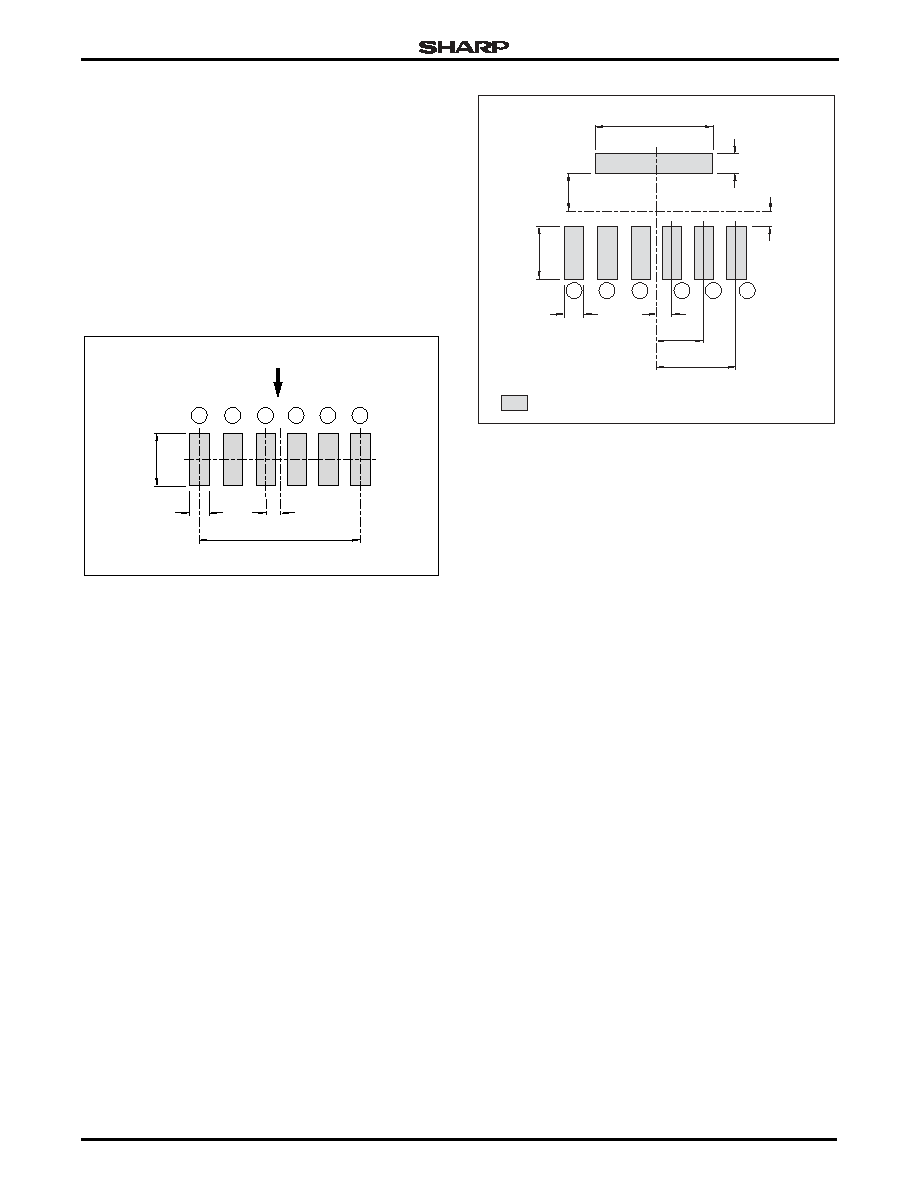
MECHANICAL DESIGN TIPS
Recommended Footprint
Figure 10 shows the recommended footprint for
PCB design when using the SHARP GP2W0004YP
infrared transceiver module. All values in the figure are
applicable as a design reference and are in mm.
Figure 8. Basic System Block Diagram
GP2W0004YP-9
ENCODER
CIRCUIT
2
3
4
1
5
DECODER
CIRCUIT
Figure 9. Basic System Waveforms
NOTES:
1 Transmit data waveform
2 Encoder circuit output waveform
3 Transmitter output optical signal waveform
4 GP2W0004YP receiver output waveform
5 Receive data waveform
1
Data Rate
T =
Data rate: 2.4 kbit/s, 9.6 kbit/s, 19.2 kbit/s, 38.4 kbit/s,
57.6 kbit/s, 115.2 kbit/s
0
0
T
3/16T
1
0
1
T
3
1
2
4
5
1
0
1
GP2W0004YP-10
Figure 10. Recommended Footprint
NOTE: Dimensions are in mm.
GP2W0004YP-11
1.1
6 - 0.9
P 1.55
P 1.55 ◊ 5 = 7.75
6 - 2.6
1.1
GP2W0004YP/XP
Infrared Transceiver
6
IrDA Technical Information
Solder Paste Footprint
T h e s o l d e r p a s t e f o o t p r i n t d r a w i n g f o r
GP2W0004YP is shown in Figure 11. Note that the
shield contact for GP2W0004YP is applied through the
Ground pin in position 6. The shield is soldered to the
back of the transceiver at the ground pin, and a sepa-
rate contact for a ground tab is not required.
T h e s o l d e r p a s t e f o o t p r i n t d r a w i n g f o r
GP2W0004XP is shown in Figure 12.
For complete mechanical dimensions, refer to the
full specification.
Figure 11. GP2W0004YP Solder Paste Footprint
0.85
2.3
0.775
P 1.55 ◊ 5 = 75
NOTE: Viewed from the parts side of PCB.
LENS (PD/LED) SIDE
GP2W0004YP-1
1
2
3
4
5
6
Figure 12. GP2W0004XP Solder Paste Footprint
0.85
1. Dimensions are in mm.
2. Soldering paste area.
NOTES:
2.3
1.825
0.775
0.80
0.775
2.325
5.60
3.875
6
5
4
3
2
1
GP2W0004YP-15

Infrared Transceiver
GP2W0004YP/XP
IrDA Technical Information
7
Designing the IR Cosmetic Window
Figure 13 provides example calculations and design
hints for IR cosmetic windows with viewing angles of
±18∞ in both the vertical and horizontal axes. All values
given here for the transceiver dimensions are only for
design reference and are in mm.
The optical window size should be the minimum size
of W ◊ H, rectangular or elliptical, in order to not reduce
IrDA data transfer performance. The dimensions for W
can be calculated by the formula:
W = 2 ◊ L ◊ tan 18 + w
and the dimensions for H can be calculated by the
formula:
H = 2 ◊ L ◊ tan 18 + h
in the case where the viewing angle is +18∞, which
conforms to or exceeds the IrDA Serial Infrared Physi-
cal Layer Link Specification. Any values to be calcu-
lated with these formula must be given in mm.
Figure 13. IR Window Cosmetic Design
w
(8.475)
18
∞
18
∞
L
W
NOTE: Dimensions are in mm.
GP2W0004YP-12
h
(3.15)
H
L
18
∞
18
∞
GP2W0004YP/XP
Infrared Transceiver
8
IrDA Technical Information
Product Packaging
Many products that use infrared communication
locate their reception component behind dark plastic.
This often fits in with the overall design and coloring of
the product and has an intentional design purpose as
well.
The photodiode that is used in optical receivers is
sensitive to a range of light wavelengths, not only the
wavelength intended for reception. Visible light has
many component factors and sources in a room. The
dark plastic used in product faceplates can be formu-
lated to act as a highpass filter, reducing the amount of
visible light and other wavelengths landing on the pho-
todiode and raising the internal noise currents.
The reduction of unwanted wavelengths provides for
a quieter and more sensitive receiver. The wavelength
used for IrDA data communication is 880 nm.
The characteristic of any plastic used in a final product
should be kept in mind and not attenuated at this wave-
length.
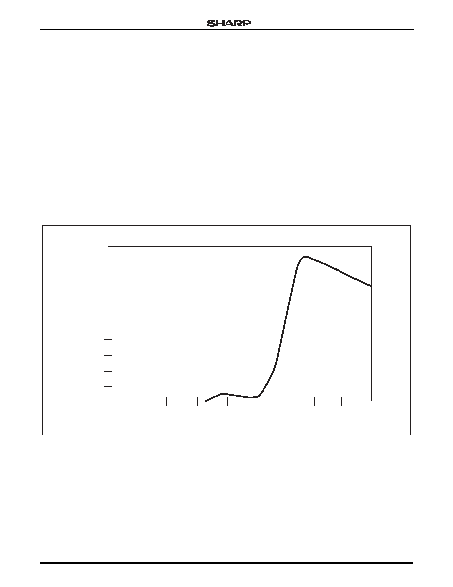
Figure 14 shows the basic characteristic of a high-
pass filter. The exact position of the slope and increas-
ing response will depend on the material selected. The
intent is to surprise visible light and neighboring wave-
lengths, and pass the desired 880 nm.
Plastic filters are available on the market, and ven-
dors carry plastic materials that may be cut, bent, or
molded. The key to selecting a plastics vendor is to ask
about the wavelength characteristics of the materials.
The more the vendor knows, the more likely the vendor
will be able to help you in a knowledgeable manner
when working on both the industrial design and wave-
length pass characteristics of your IR window. If the
vendor does not know what you are talking about, you
need to find a knowledgeable source for filter materials.
Figure 14. Highpass Filter Characteristics
GP2W0004YP-13
100
90
80
70
60
RESPONSE % TRANSMISSION
ULTRAVIOLET
VIOLET
BLUE-GREEN
GREEN
YELLOW
ORANGE
RED
50
40
30
20
10
0
300
400
500
600
700
800
900
1,000
1,100
WAVELENGTH, nm

Infrared Transceiver
GP2W0004YP/XP
IrDA Technical Information
9
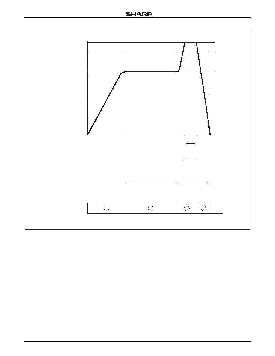
Soldering Reflow Profile
Figure 15 is a straight-line representation of the rec-
ommended temperature profile for the IR solder reflow
process. The temperature profile is divided into four
process sections with three temperature/time change
rates. The temperature/time details are described in
Table 3.
I n p r o c e s s s e c t i o n 1 , t h e P C B a n d S M D
GP2W0004YP molded pinout joints are heated to a
temperature of 165∞C to activate the flux in the solder
paste. The temperature ramp-up rate R1 should be
within the range of 1∞C to 5∞C per second. Package
temperature must be kept within the temperature range
specified in order to avoid localized temperature rise in
the resin.
In process section 2, sufficient time to dry the solder
paste should be provided, a maximum of 120 seconds
is recommended for optimum results. A stable temper-
ature is recommended with little temperature increase,
preferably staying at the level of 165∞C.
Process section 3 is solder reflow. The temperature
should be raised to 240∞C for 10 seconds, at the rate of
1∞C to 4∞C per second (R2) for the desired result. The
dwell time above 200∞C must not exceed 60 seconds.
Beyond 60 seconds, weak and unreliable connections
will result.
Process section 4 is cooling. After solder reflow, the
temperature should then be reduced at the rate of -1∞C
to -4∞C per second (R3). Please note that deformation
of the PCB can also affect the pins of the package,
which may break the gold wire used in the transceiver
module. Full confirmation of the soldering reflow
machine condition is highly recommended for optimal
results.
Hand soldering should be conducted with a soldering
iron of less than 25 W, at less than 300∞C. Soldering
time is less than 5 seconds per contact, with a second
or two between soldering each contact. The device
being soldered by hand should be at room temperature.
Use 60/40 or 63/37 solder, or Ag solder if it is available.
Table 3. Process Section Information
PROCESS SECTION
TEMPERATURE
SYMBOL
TERMPERATURE/TIME MAX.
1. Heat Up
~165∞C
R1
1∞C - 5∞C/sec. MAX.
2. Solder Paste Dry
165∞C
3. Solder Reflow
165∞C - 240∞C
R2
1∞C - 5∞C/sec. MAX.
4. Cooling
~200∞C
R3
-1∞C - 4∞C/sec. MAX.
GP2W0004YP/XP
Infrared Transceiver
10
IrDA Technical Information
Figure 15. IR Solder Reflow Temperature Profile
200
∞
C
240
∞
C MAX.
165
∞
C MAX.
25
∞
C
50
∞
C
100
∞
C
150
∞
C
120 sec. MAX.
NOTE:
1. Heat Up
2. Solder Paste Dry
3. Solder Reflow
4. Cooling
90 sec. MAX.
10 sec.
MAX.
60 sec.
MAX.
R3
R1
TEMPERA
TURE
∞
C
PROCESS SECTIONS
TIME
R2
1
2
3
4
GP2W0004YP-16

Infrared Transceiver
GP2W0004YP/XP
IrDA Technical Information
11
Evaluation Board
The circuit diagram in Figure 16 is the recom-
mended evaluation circuit for the GP2W0004YP. This
circuit is provided on an evaluation board for test and
evaluation purposes. Samples are available through
your Sharp support office, Sales Representative, or
Distributor.
The resistor value for R
L
is selected based on the
supply voltage. The 5.1
value is selected for V
LEDA
between 3.6 V and 4.5 V, and has been loaded on the
test boards as a nominal value. Adjust it for your oper-
ating conditions per Table 4.
The forward current through the LED is adjusted by
the resistor value and directly controls the operating
range of the LED.
The capacitor values shown on the board are nomi-
nal for this test application. The final values are depen-
dent on the amount and frequency of noise in the final
system. Capacitor values need to be properly tailored
for the end application.
This test and evaluation board is not intended for
production applications and should be used for test and
evaluation purposes only.
Table 4. R
L
Value
RESISTOR VALUE
LED SUPPLY VOLTAGE (V
LEDA
)
RANGE
1.0
at 0.5 Watt
2.4
V
LEDA
3.3 V
3.0
at 0.5 Watt
3.0
V
LEDA
3.6 V
5.1
at 0.5 Watt
3.6
V
LEDA
4.5 V
7.5
at 0.5 Watt
4.5
V
LEDA
5.5 V
Figure 16. GP2W0004YP Recommended Evaluation Circuit
GP2W0004YP-14
LEDA
TXD
RXD
SD
V
CC
GND
+
+
+
+
+
+
+
+
+
+
1
2
3
4
5
6
3
5
7
9
1
2
4
6
8
10
V
CC
TXD
RXD
GP2W0004YP
CX
1
22 µF
CX
2
0.1 µF
R
L
5.1
, 1/2 W
J1
GND
SD
2 ◊ 5

GP2W0004YP/XP
Infrared Transceiver
12
IrDA Technical Information
PACKING INFORMATION
This section describes the GP2W0004YP moisture-
proof packing and is only for reference. The same sec-
tion of the official specifications should be consulted for
detailed packing information.
Packing Specifications
PACKING MATERIAL
The GP2W0004YP reel is moisture-proof packed for
shipment. Table 5 describes the materials used for
each item of the moisture-proof packing.
TAPE AND REEL
Figures 17 through 19 show the reel dimensions and
product orientation in the reel.
G P 2 W 0 00 4 Y P i s th e s i d e v i ew de v i c e , a n d
GP2W0004XP is the top view device. Note that the
device orientation in the reel is not the same for both
devices.
Table 5. Packing Materials
ITEM
MATERIAL
Aluminum Laminate Bag
Aluminum Polyethylene
Label
Paper
Desiccant
Outer Case
Paper
Pads
Paper
Figure 17. Reel Structure and Dimensions
330
±2
13
±0.2
2
±0.5
22.5 MAX.
21
±0.8
17.5
±0.5
100
±0.1
GP2W0004YP-17
NOTE:
Dimensions are in mm.

Infrared Transceiver
GP2W0004YP/XP
IrDA Technical Information
13
ORDERING INFORMATION
Table 6 shows the correct ordering information for the
device in both the top view and side view orientation.
Figure 18. Direction of Product Insertion (GP2W0004YP)
Figure 19. Direction of Product Insertion (GP2W0004XP)
GP2W0004YP-18
LENS
SIDE
PULL-OUT DIRECTION
LABEL
GP2W0004YP-19
PULL-OUT DIRECTION
LABEL
Table 6. Ordering Information
MODEL NUMBER
ORIENTATION
PACKAGING
GP2W0004YP
Side View
Tape and Reel
GP2W0004XP
Top View
Tape and Reel
GP2W0004YP/XP
Infrared Transceiver
14
IrDA Technical Information
Packing Method
Table 7 provides information on how each tape reel
is packaged. Each aluminum laminate bag contains
one reel (2,000 devices per reel) and desiccant. Four
reels in their bags are packed per carton (4 reels/car-
ton; 8,000 transceivers per carton).
The outer carton will then be sealed with craft tape,
with indication of model name, quantity, and outgoing
inspection date on the case.
Storage Conditions
The product should be stored with these conditions:
∑ Storage temperature: 10∞C to 30∞C
∑ Humidity: below 60% RH
Treatment After Opening
After unsealing, devices should be mounted within
the temperature condition of 10∞C to 30∞C, at the
humidity condition below 60% RH, within 3 days
(72 hours).
If long-term storage is needed, devices should either
be stored in a dry box or re-sealed in a moisture-proof
bag with desiccant and stored in an environment where
the temperature is 10∞C to 30∞C at the humidity condi-
tion of below 60% RH. Devices must be mounted within
two weeks.
Baking Before Mounting
In the event that the devices are not maintained in
the storage conditions described, or the enclosed des-
iccant indicator has turned pink in color, baking must be
done before devices are to be mounted. Also note that
devices should only be baked once.
These devices are hydroscopic, in that the plastic resin will ab-
sorb moisture. If the resin absorbs too much moisture, it will
undergo rapid mechanical expansion when passed through
the IR reflow process. This can cause device failures. The res-
in material from all device vendors has this characteristic.
CAUTION
Baking should be done with the devices removed from the
reel, as the reel will melt. To complete the baking properly, de-
vices should either be temporarily mounted to a PCB with ad-
hesive or placed in a metal tray. Any device that has been out
of dry pack for more than 72 hours should be dried in some
manner prior to any surface mount reflow process. Otherwise
these devices should be mounted and soldered by hand.
Recommended temperature: 100∞C, 12 to 24 hours.
CAUTION
Table 7. Packing Methods
PACKING
SHAPE
PRODUCT
QUANTITY
PER REEL
QUANTITY
PER BAG
QUANTITY
PER CARTON
Tape reel
(
300 mm)
1 model
2,000 pieces
per reel
1 reel per
laminated bag
4 reels
per carton

GP2W0004YP/XP
Infrared Transceiver
©2002 by SHARP Corporation
Reference Code SMA02025
SPECIFICATIONS ARE SUBJECT TO CHANGE WITHOUT NOTICE.
Suggested applications (if any) are for standard use; See Important Restrictions for limitations on special applications. See Limited
Warranty for SHARP's product warranty. The Limited Warranty is in lieu, and exclusive of, all other warranties, express or implied.
ALL EXPRESS AND IMPLIED WARRANTIES, INCLUDING THE WARRANTIES OF MERCHANTABILITY, FITNESS FOR USE AND
FITNESS FOR A PARTICULAR PURPOSE, ARE SPECIFICALLY EXCLUDED. In no event will SHARP be liable, or in any way responsible,
for any incidental or consequential economic or property damage.
NORTH AMERICA
EUROPE
JAPAN
SHARP Microelectronics of the Americas
5700 NW Pacific Rim Blvd.
Camas, WA 98607, U.S.A.
Phone: (1) 360-834-2500
Fax: (1) 360-834-8903
www.sharpsma.com
SHARP Microelectronics Europe
Division of Sharp Electronics (Europe) GmbH
Sonninstrasse 3
20097 Hamburg, Germany
Phone: (49) 40-2376-2286
Fax: (49) 40-2376-2232
www.sharpsme.com
SHARP Corporation
Electronic Components & Devices
22-22 Nagaike-cho, Abeno-Ku
Osaka 545-8522, Japan
Phone: (81) 6-6621-1221
Fax: (81) 6117-725300/6117-725301
www.sharp-world.com
TAIWAN
SINGAPORE
KOREA
SHARP Electronic Components
(Taiwan) Corporation
8F-A, No. 16, Sec. 4, Nanking E. Rd.
Taipei, Taiwan, Republic of China
Phone: (886) 2-2577-7341
Fax: (886) 2-2577-7326/2-2577-7328
SHARP Electronics (Singapore) PTE., Ltd.
438A, Alexandra Road, #05-01/02
Alexandra Technopark,
Singapore 119967
Phone: (65) 271-3566
Fax: (65) 271-3855
SHARP Electronic Components
(Korea) Corporation
RM 501 Geosung B/D, 541
Dohwa-dong, Mapo-ku
Seoul 121-701, Korea
Phone: (82) 2-711-5813 ~ 8
Fax: (82) 2-711-5819
CHINA
HONG KONG
SHARP Microelectronics of China
(Shanghai) Co., Ltd.
28 Xin Jin Qiao Road King Tower 16F
Pudong Shanghai, 201206 P.R. China
Phone: (86) 21-5854-7710/21-5834-6056
Fax: (86) 21-5854-4340/21-5834-6057
Head Office:
No. 360, Bashen Road,
Xin Development Bldg. 22
Waigaoqiao Free Trade Zone Shanghai
200131 P.R. China
Email: smc@china.global.sharp.co.jp
SHARP-ROXY (Hong Kong) Ltd.
3rd Business Division,
17/F, Admiralty Centre, Tower 1
18 Harcourt Road, Hong Kong
Phone: (852) 28229311
Fax: (852) 28660779
www.sharp.com.hk
Shenzhen Representative Office:
Room 13B1, Tower C,
Electronics Science & Technology Building
Shen Nan Zhong Road
Shenzhen, P.R. China
Phone: (86) 755-3273731
Fax: (86) 755-3273735