
IrDA Technical Information
1
GP2W0116YPS/118YPS
IrDA Technical Information
Compact Transceiver
FEATURES
∑ IrDA Low Power Option Compatibility for Telecom-
munication and Mobile Terminals
∑ Low Volume Package Design
≠ 7.2 (W) ◊ 2.75 (D) ◊ 1.85 (H) mm, 36.6 mm
3
∑ Low Current Receive Mode, 90
µ
A TYP.
∑ Built-in Shut-Down Mode (0.001
µ
A TYP.)
∑ Internal LED Current Regulator.
≠ V
DD
= 2.0 V - 3.6 V, V
LEDA
= 2.0 - 6.0 V
≠ External LED Current Limiting Resistor not Required
∑ Soldering Reflow Capable
∑ SMD Lead-less Packages For Either Vertical Mount
or Horizontal Mount to PCBs
∑ Added Features include Tri-state Output and Split-
Voltage Supply Capability
∑ Top View Version: GP2W0118YPS
APPLICATIONS
∑ Telecommunication Products
≠ Cellular Phones
≠ Pagers
≠ Smart Phones
∑ Mobile Products
≠ PDAs
≠ Electronic Wallets
∑ Imaging Products
≠ Portable Printers
≠ Portable Text Scanners
DESCRIPTION
The SHARP GP2W0116YPS is a low-power, short-
range infrared transceiver module. It meets the Mobile
Communication low power option within the IrDA Spec-
ifications for the 20 cm communication range. This unit
provides the interface between logic and IR signals for
through-air, serial, half-duplex IR wireless data links at
rates up to 115 kbit/s and is designed to satisfy the IrDA
physical layer (PHY) specifications.
The SHARP GP2W0116YPS infrared transceiver
module contains a high speed, high efficiency, low power
consumption AlGaAs LED, silicon PIN photodiode, and
low power bipolar integrated circuit. The IC contains a
LED driver circuit and a receiver that provides the RX
output supporting 2.4 kbit/s to 115.2 kbit/s IrDA signals,
meeting the IrDA low power option communication stan-
dard (0.2 m link distance with low powered devices and
0.3 m link distance with standard devices.)
The GP2W0116YPS includes a constant current
source in the LED driver circuit that eliminates the need
for an external current limiting resistor in the LED circuit.
The low power option specification is an excellent
choice for telecommunication products and mobile ter-
minals, such as mobile phones, paging devices, and
PDA-cellular combined multimedia devices. The trans-
ceiver module provides wireless data link capability for
mobile phones and pagers, PDAs, or any other IrDA
application already introduced to the marketplace.
The transceiver module receiver electronics operate
at 2.0 V through 3.6 V without any performance degra-
dation. The split-voltage supply allows the LED voltage
to come from a separate supply. For example, in a cell
phone the LED may operate from the battery, while the
receiver and logic section is supplied from a lower volt-
age regulated supply.
This enables an energy-saving design in any appli-
cation field, with alternatives for supply voltage and
flexibility for other components. The GP2W0116YPS
transceiver module has a built-in 0.001
µ
A shutdown
mode for those applications that are very conscious
about current consumption. The GP2W0116YPS also
has a tri-state output, which allows its use in applica-
tions where one I/O port connection may be connected
to more than one I/O device.
The shield is appropriate in applications where Elec-
tro-Magnetic Interference (EMI) is a concern. Infrared
energy is immune to EMI; however, the receiving PIN
photodiode is somewhat sensitive to EMI. This is the
case in all IR communication devices.

GP2W0116YPS/118YPS
Compact Transceiver
2
IrDA Technical Information
PACKAGE
The dimensional drawing and all packaging informa-
tion is available in the specification, which is available
from your Sharp Components representative. The
specification will have the most up-to-date information.
ABSOLUTE MAXIMUM RATINGS
NOTE: *See the Soldering Reflow Profile section.
RECOMMENDED OPERATING CONDITIONS
NOTE: *Bit rate = 115 kbit/s (in-band signals). An in-band optical signal is a pulse/sequence
where the peak wavelength,
P, is defined as 850 nm
P
900 nm, and the pulse
characteristics comply with IrDA Serial Infrared Physical Layer Link Specifications.
Table 1. Pin Names
PIN NO.
DESCRIPTION
SYMBOL
1
Supply Voltage
V
DD
2
Ground
GND
3
Shutdown
SD
4
Receiver Data Output
RXD
5
Transmitter Data Input
TXD
6
LED Anode
LEDA
Figure 1. Package Orientation
PIN 1
FRONT VIEW
REAR VIEW
PIN 6
PIN 6
PIN 1
GP2W0116YPS-3
PARAMETER
SYMBOL MIN. MAX. UNIT
Supply Voltage
V
DD
0
6.0
V
LED Supply Voltage
V
LEDA
0
7.0
V
Peak Forward LED Current
I
FM
60
mA
Operating Temperature
T
OPR
-40
+85
∞C
Storage Temperature
T
STG
-40
+85
∞C
Soldering Temperature*
T
SOL
260
∞C
PARAMETER
SYMBOL
MIN.
MAX.
UNIT
CONDITIONS
Supply Voltage
V
DD
2.0
3.6
V
LED Supply Voltage
V
LEDA
2.0
6.0
V
Logic HIGH Shut-down Terminal Input Voltage
V
IHSD
V
DD
◊ 0.67
V
DD
V
Shutdown Mode
Logic LOW Shut-down Terminal Input Voltage
V
ILSD
0.0
V
DD
◊ 0.1
V
Normal Mode
Logic HIGH Transmitter Input Voltage (TXD)
V
IHTXD
V
DD
◊ 0.80
V
DD
V
LED ON
Logic LOW Transmitter Input Voltage (TXD)
V
ILTXD
0.0
V
DD
◊ 0.2
V
LED OFF
Logic HIGH Receiver Input Irradiance*
E
IH
0.081
mW/cm
2
Receiver Signal Rate
BR
2.4
4,000
kbit/s
Operating Temperature
T
OPR
0
70
∞C
25∞C TYP.

Compact Transceiver
GP2W0116YPS/118YPS
IrDA Technical Information
3
ELECTRICAL AND OPTICAL
SPECIFICATIONS
Specifications in Table 2 hold over the Recom-
mended Operating Conditions, unless otherwise noted.
All typical values are at 25∞C, and V
DD
= 2.0 V to 3.6 V,
unless otherwise noted. Refer to the specifications for
complete details and conditions.
NOTE: *I
OL
current goes into IC while RXD is ON state.
Table 2. Electrical and Optical Specifications
PARAMETER
SYMBOL
MIN.
TYP. MAX.
UNIT
CONDITIONS
Maximum Reception Distance
L
0.2
m
2
1/2
15∞, I
E
3.3 mW/sr
High Level Output Voltage
V
OHRXD
V
DD
≠ 0.4
V
I
OH
= 20
µ
A
Low Level Output Voltage*
V
OLRXD
0.45
V
I
OL
= 20
µ
A
Viewing Angle
2
30
degrees
Low Level Pulse Width
tw
1.28
6.0
µ
s
BR = 115.2 kbit/s, 2
1/2
15∞
Current Consumption
I
DD
90
120
µ
A
With no input signal, SD = 0 V,
Output Terminal Open
I
DD-S
0.001
0.1
µ
A
Shutdown Mode, no input signal,
V
IHSD
= V
DD
≠ 0.5 V,
Output Terminal Open,
T
OPR
= 25∞C, V
DD
= 3.3 V
Rise Time
tr
0.06
µ
s
See Figure 2
Fall Time
tf
0.06
µ
s
See Figure 2
Latency
t
TAT
25
300
µ
s
Receiver Wakeup Time
tsdw
200
µ
s
No input signal
Radiant Intensity
I
E
4.0
25
mW/sr
2
1/2
15∞, BR = 115.2 kbit/s,
V
LEDA
= 3.3 V, V
IHTXD
= 2.8 V
Peak Emission Wavelength
p
850
870
900
nm
Peak LED Current
I
LED
25
32
40
mA
Shutdown Input Current
lisd
-0.02
0
+0.02
mA
T
OPR
= 25∞C, V
DD
= 3.3 V
Figure 2. Infrared Transceiver Module Output
90%
V
OH
50%
10%
CRITERIA FOR
PULSE POSITION
V
OL
t
F
t
R
t
W
GP2W0116YPS-1

GP2W0116YPS/118YPS
Compact Transceiver
4
IrDA Technical Information
ELECTRICAL DESIGN APPLICATION TIPS
The only external component needed for the
GP2W0116YPS is a capacitor for filtering power supply
noise. See the Mechanical Design Hints section for
technical reference data in optical/electrical character-
istics. An optional resistor can be added in series with
the V
DD
line if the system power supply is noisy and
additional filtering is required. A resistor value of 1
-
15
is suggested, depending on the amount of filtering
required.
Application Circuit and External
Components
Figure 3 shows the recommended application circuit.
V
LEDA
may be connected to V
DD
or driven sepa-
rately from a different voltage source that is within the
allowed range. The recommended operating voltage
range for V
DD
is 2.0 V to 3.6 V, and the operating range
for V
LEDA
is 2.0 to 6.0 V.
An example of the split voltage source design is
shown in Figure 4. In the figure, the V
DD
pin is used to
provide power to the receiver electronics. This inter-
face can be at a lower potential than the voltage used
to source the LED.
The V
LEDA
voltage may be directly driven from the
battery in the above design example. The V
DD
associ-
ated with the receiver interface electronics may be sup-
ported by a power regulator or other device providing
an efficient regulated lower voltage source. This volt-
age may be as low as 2.0 V to 3.6 V, and the V
LEDA
potential may range from 2.0 V to 6.0 V.
An alternative is to connect the V
LEDA
and V
DD
pins
together as shown in Figure 5. This arrangement allows
the GP2W0116YPS to be used in previous applications
where both of these voltage sources are connected.
Figure 3. Application Circuit
GP2W0116YPS-4
CX
GND
SD
SD
GND
V
DD
V
DD
TXD
TXD
RXD
RXD
LEDA
LEDA
+
COMPONENT
NOTE: CX value should be adjusted in accordance
with the noise level and the power supply frequency.
RECOMMENDED VALUE
CX
10
µ
F/6.3 V (NOTE)
1
2
3
4
5
6
Figure 4. Split Voltage Source
Figure 5. Combined Voltage Source
RECEIVER
INTERFACE
ELECTRONICS
RXD
V
LEDA
V
DD
TXD
SD
GP2W0116YPS-5
RECEIVER
INTERFACE
ELECTRONICS
RXD
V
LEDA
V
DD
TXD
SD
GP2W0116YPS-6

Compact Transceiver
GP2W0116YPS/118YPS
IrDA Technical Information
5
Shutdown Mode
The `Shutdown' pin is an active HIGH terminal and
performs the power saving function in accordance with
Figure 6 and Table 3.
Signal Waveform Example
Figure 9 shows the waveform at each point in the
block diagram while operating the GP2W0116YPS in a
manner conforming to IrDA standards. The waveform
example is only applicable as a design and evaluation
reference to understand the GP2W0116YPS hardware
implementation and system measurement.
Table 3. Shutdown Modes
INPUT
PERFORMANCE
HIGH
Shutdown Mode
LOW
Normal Operation Mode
OPEN
Normal Operation Mode
Figure 6. Shutdown-Receiver Wake Up Time
Table 4. Shutdown Truth Table
SD
TXD
LED
RECEIVER
TR1
TR
2
RXD
LOW
HIGH
On
Don't Care
Pull-up
LOW
Off
IrDA Signal
Off
On
LOW
No Signal
On
Off
HIGH
HIGH
Don't
Care
Off
Don't Care
Off
Off
Pull-up
Figure 7. RXD Output Configuration
SD
RXD
OPERABLE
SHUTDOWN
ENABLED
V
IH
V
IL
HIGH
(or OPEN)
LOW
0.2 ms
GP2W0116YPS-7
TR1
TR2
260 k
TYPICAL
RXD
GP2W0116YPS-2
Figure 8. Basic System Diagram
Figure 9. Basic IrDA Waveforms
ENCODER
CIRCUIT
DECODER
CIRCUIT
GP2W0116YPS-8
3
1
2
4
5
NOTES:
1 Transmit data waveform
2 Encoder circuit output waveform
3 Transmitter output optical signal waveform
4 GP2W0116YP receiver output waveform
5 Receiver data waveform
1
Data Rate
t
=
Data rate: 2.4 kbit/s, 9.6 kbit/s, 19.2 kbit/s, 38.4 kbit/s,
57.6 kbit/s, 115.2 kbit/s
0
0
t
3/16t
1
0
1
t
3
1
2
4
5
1
0
1
GP2W0116YPS-9

GP2W0116YPS/118YPS
Compact Transceiver
6
IrDA Technical Information
MECHANICAL DESIGN HINTS
Recommended Footprint
Figure 10 shows the recommended footprint dimen-
sions that may also be used for the solder mask stencil.
Note that the footprint spacing for the electrical con-
tacts is the same. The position of the ground tab con-
nection between the side view (GP2W0116YPS) and
the top view (GP2W0118YPS) orientation are different.
For ground tab connections, pin 7 should be connected
to the ground plane associated with the power connec-
tion for the IrDA device. The center of the device
mounting position is also slightly shifted between the
two drawings. Figure 11 shows a composite footprint
that may be used when both devices are mounted on
the same footprint for multiple applications.
Figure 10. Footprint Dimensions
Figure 11. Composite Footprint
3.0
7
0.6
0.6
0.8
3.95
0.475
VIEW FROM COMPONENT SIDE
Pin shown for position reference,
Pin is Shield Ground
GP2W0116YPS
LENS (PD/LED) SIDE
GP2W0118YPS
LENS (PD/LED) SIDE
1.425
1.425
0.475
2.375
2.375
1.1
1.55
0.85
1.40
0.25
0.1
1.55
2.0
7
7
1
1
7
VIEW FROM COMPONENT SIDE
Pin shown for position reference,
Pin is Shield Ground
1
7
1
GP2W0116YPS-11
NOTE: Dimensions are in mm.
GP2W0116YPS-13
NOTES:
1. Solder paste not needed when using GP2W0118YPS.
2. Solder paste not needed when using GP2W0116YPS.
3. Dimensions are in mm.
4. Pin shown for position reference.
5. Pin is Shield Ground
0.85
1.40
0.6
1.55
1.425
3.0
0.475
2.375
3.95
1.1
2.0
0.25
0.10
0.8
See
Note 1
BODY CENTER
for GP2W0118YPS
BODY CENTER
for GP2W0116YPS
See
Note 2
See
Note 2
7
7
7
1
1
7

Compact Transceiver
GP2W0116YPS/118YPS
IrDA Technical Information
7
Designing the IR Cosmetic Window
Figure 12 provides example calculations and design
hints for IR cosmetic windows with viewing angles of
±18∞ in both the vertical and horizontal axes. All values
given here for transceiver dimensions are only for refer-
ence. Consult the current data sheet for specifications.
The IrDA specifications require a ±15∞ viewing angle at
the transceiver. The ±18∞ angle shown here provides a
little extra clearance to allow for slight manufacturing
variations and that the required angle is always met.
The optical window size should be the minimum size
of W ◊ H, rectangular or elliptical, to have the best IrDA
data transfer performance. The dimensions for W can
be calculated by the formula:
W = 2 ◊ L ◊ tan18 + w
and the dimensions for H can be calculated by the
formula:
H = 2 ◊ L ◊ tan18 + h
in the case of having a viewing angle of 18∞, which con-
forms to or exceeds the IrDA Serial Infrared Physical
Layer Link Specifications. Values calculated with the for-
mula are in mm. The dimension `7.9' in Figure 12 is the
physical length of the transceiver. This distance includes
the side angles of the optical lenses to simplify the over-
all calculation. The height of the transceiver is 2.0 mm
with the shield.
Product Packaging
Many products that use infrared communication locate
their reception component behind dark plastic. This often
fits in with the overall design and coloring of the product
and has an intentional design purpose as well.
The photodiode that is used in optical receivers is
sensitive to a range of light wavelengths, not only the
wavelength intended for reception. Visible light has
many component factors and sources in a room. The
dark plastic used in product faceplates can be formu-
lated to act as a highpass filter, reducing the amount of
visible light and other wavelengths landing on the pho-
todiode and raising the internal noise currents.
The reduction of unwanted wavelengths provides for
a quieter and more sensitive receiver. The wavelength
used for IrDA data communication is 880 nm. The char-
acteristic of any plastic used in a final product should be
kept in mind and not attenuated at this wavelength.
Glass and plastic filters are available on the market,
and vendors carry plastic materials that may be cut,
bent, or molded. The key to selecting a plastics vendor
is to ask about the wavelength characteristics of the
materials. The more the vendor knows, the more likely
the vendor will be able to help you in a knowledgeable
manner when working on both the industrial design and
wavelength characteristics of your IR window. If the
vendor does not know what you are talking about, you
need to find a more knowledgeable source for filter
materials.
Figure 12. IR Window Cosmetic Design
w
(7.9)
18
∞
18
∞
18
∞
18
∞
L
W
NOTE: Dimensions are in mm.
h
(2.0)
H
L
GP2W0116YPS-12

GP2W0116YPS/118YPS
Compact Transceiver
8
IrDA Technical Information
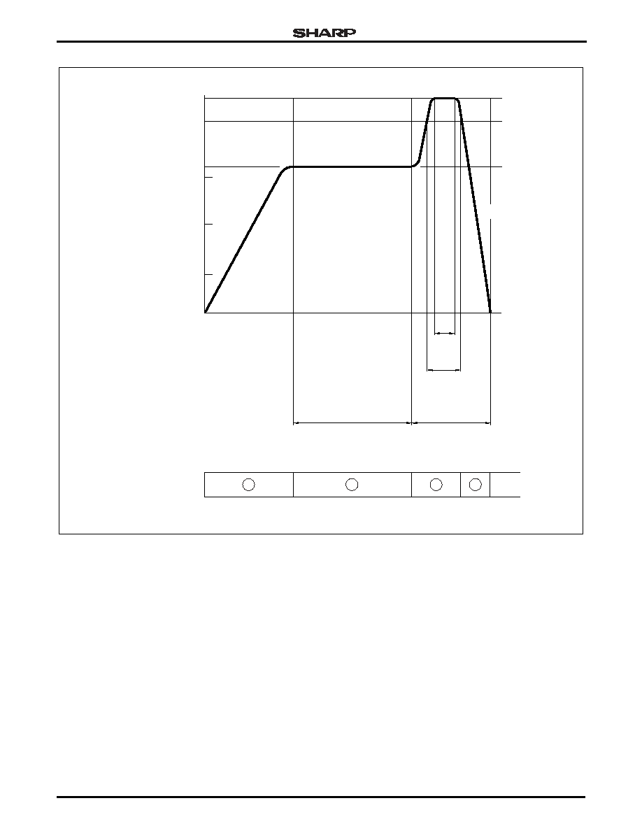
SOLDERING REFLOW PROFILE
Figure 13 is a straight-line representation of the rec-
ommended temperature profile for the IR solder reflow
process. The temperature profile is divided into four
process sections with three temperature/time change
rates. The temperature/time details are described in
Table 5.
I n p r o c e s s s e c t i o n 1 , t h e P C B a n d S M D
GP2W0116YPS molded pinout joints are heated to a
temperature of 165∞C to activate the flux in the solder
paste. The temperature ramp-up rate R1 should be
within the range of 1∞C to 5∞C per second. Package
temperature must be kept within the temperature range
specified in order to avoid localized temperature rise in
the resin by the infrared lamp.
In process section 2, sufficient time to dry the solder
paste should be provided, a maximum of 120 seconds
is recommended for optimum results. A stable temper-
ature is recommended with little temperature increase,
preferably staying at the level of 165∞C.
Process section 3 is solder reflow. The temperature
should be raised to 260∞C for 5 seconds, at the rate of
1∞C to 4∞C per second (R2) for the desired result. The
dwell time above 200∞C must not exceed 60 seconds.
Beyond 60 seconds, weak and unreliable connections
will result. The temperature should then be reduced at
the rate of -1∞C to -4∞C per second (R3). Please note
that deformation of the PCB can also affect the pins of
the package, which may break the gold wire used in the
transceiver module. Full confirmation of the soldering
reflow machine condition is highly recommended for
optimal results.
Hand soldering should be conducted with a soldering
iron of less than 25 W, at less than 300∞C. Soldering
time is less than 5 seconds per contact, with a second
or two between soldering each contact. The device
being soldered by hand should be at room temperature.
Use 60/40 or 63/37 solder, or Ag solder if it is available.
Table 5. Process Step Information
SECTION
TEMPERATURE SYMBOL TERMPERATURE/TIME MAX.
Heat Up
~165∞C
R1
1∞C - 5∞C/sec. MAX.
Solder Paste Dry
165∞C
Solder Reflow
165∞C - 230∞C
R2
1∞C - 5∞C/sec. MAX.
Cooling
~200∞C
R3
-1∞C - 4∞C/sec. MAX.
Compact Transceiver
GP2W0116YPS/118YPS
IrDA Technical Information
9
Figure 13. Solder Reflow Profile
200
∞
C
260
∞
C MAX.
165
∞
C MAX.
25
∞
C
50
∞
C
100
∞
C
150
∞
C
120 sec. MAX.
NOTE:
1. Heat Up
2. Solder Paste Dry
3. Solder Reflow
4. Cooling
90 sec. MAX.
5 sec.
MAX.
60 sec.
MAX.
R3
R1
TEMPERA
TURE
∞
C
PROCESSES
TIME
R2
1
2
3
4
GP2W0116YPS-10

GP2W0116YPS/118YPS
Compact Transceiver
©2002 by SHARP Corporation
Reference Code SMA02050
SPECIFICATIONS ARE SUBJECT TO CHANGE WITHOUT NOTICE.
Suggested applications (if any) are for standard use; See Important Restrictions for limitations on special applications. See Limited
Warranty for SHARP's product warranty. The Limited Warranty is in lieu, and exclusive of, all other warranties, express or implied.
ALL EXPRESS AND IMPLIED WARRANTIES, INCLUDING THE WARRANTIES OF MERCHANTABILITY, FITNESS FOR USE AND
FITNESS FOR A PARTICULAR PURPOSE, ARE SPECIFICALLY EXCLUDED. In no event will SHARP be liable, or in any way responsible,
for any incidental or consequential economic or property damage.
NORTH AMERICA
EUROPE
JAPAN
SHARP Microelectronics of the Americas
5700 NW Pacific Rim Blvd.
Camas, WA 98607, U.S.A.
Phone: (1) 360-834-2500
Fax: (1) 360-834-8903
www.sharpsma.com
SHARP Microelectronics Europe
Division of Sharp Electronics (Europe) GmbH
Sonninstrasse 3
20097 Hamburg, Germany
Phone: (49) 40-2376-2286
Fax: (49) 40-2376-2232
www.sharpsme.com
SHARP Corporation
Electronic Components & Devices
22-22 Nagaike-cho, Abeno-Ku
Osaka 545-8522, Japan
Phone: (81) 6-6621-1221
Fax: (81) 6117-725300/6117-725301
www.sharp-world.com
TAIWAN
SINGAPORE
KOREA
SHARP Electronic Components
(Taiwan) Corporation
8F-A, No. 16, Sec. 4, Nanking E. Rd.
Taipei, Taiwan, Republic of China
Phone: (886) 2-2577-7341
Fax: (886) 2-2577-7326/2-2577-7328
SHARP Electronics (Singapore) PTE., Ltd.
438A, Alexandra Road, #05-01/02
Alexandra Technopark,
Singapore 119967
Phone: (65) 271-3566
Fax: (65) 271-3855
SHARP Electronic Components
(Korea) Corporation
RM 501 Geosung B/D, 541
Dohwa-dong, Mapo-ku
Seoul 121-701, Korea
Phone: (82) 2-711-5813 ~ 8
Fax: (82) 2-711-5819
CHINA
HONG KONG
SHARP Microelectronics of China
(Shanghai) Co., Ltd.
28 Xin Jin Qiao Road King Tower 16F
Pudong Shanghai, 201206 P.R. China
Phone: (86) 21-5854-7710/21-5834-6056
Fax: (86) 21-5854-4340/21-5834-6057
Head Office:
No. 360, Bashen Road,
Xin Development Bldg. 22
Waigaoqiao Free Trade Zone Shanghai
200131 P.R. China
Email: smc@china.global.sharp.co.jp
SHARP-ROXY (Hong Kong) Ltd.
3rd Business Division,
17/F, Admiralty Centre, Tower 1
18 Harcourt Road, Hong Kong
Phone: (852) 28229311
Fax: (852) 28660779
www.sharp.com.hk
Shenzhen Representative Office:
Room 13B1, Tower C,
Electronics Science & Technology Building
Shen Nan Zhong Road
Shenzhen, P.R. China
Phone: (86) 755-3273731
Fax: (86) 755-3273735