
GP2W2003YK/
GP2W2004YK
GP2W2003YK/GP2W2004YK
s
Absolute Maximum Ratings
s
Outline Dimensions
(Unit : mm)
IrDA Transceiver Module
Compliant with IrDA Control
1. Personal Computers
2. Input devices for PC (mouse, keyboard, joy stick)
3. Amusement equipment
4. AV equipment
5. Universal controllers
s
Features
s
Applications
1. Compliant with IrDA control
GP2W2003YK
: for peripheral Type 1
GP2W2004YK
: for peripheral Type 2
2. Low dissipation current
(Dissipation current at shut-down:MAX.1
µ
A)
3. 4 Range of LED power control
4. Long distance (approx. 8m (Min. 5m)) wireless
communication at 75kbps data rate (Radiant
intensity
=
100mW/sr) (
GP2W2003YK
)
5. Wide viewing angle (Min. 1.5m,
±
40∞) wireless
communication at 75kbps data rate (
GP2W2004YK
)
6. Low power operation : 3.3V
7. Built-in envelope detector
8. By using assistance LED (SHARP
GL710
), able to use for
Host Type. (
GP2W2003YK
)
9. RESET function to recover the receiver sensitivity
10. Optimized interface to sharp peripheral engine, an
embedded communication controller for IrDA Control
Parameter
Symbol
Rating
Unit
Supply voltage
V
CC
V
CC
0 to 6.0
V
V
∞
C
Operating temperature
T
op
-
10 to 70
∞
C
Storage temperature
T
stg
-
20 to 85
Peak forward LED current
Receiver data output current
I
FM
V
O
600
mA
Soldering temperature
T
SOL
260
∞
C
(Ta
=
25
∞
C)
*1 Refer to Fig.11
*2 For MAX. 5s at the position of 1.3mm from the resin edge.
*2
*1
AV
CC
SD
RESET
GND
V
CC
V
O
TXD
T
X
CNT1
T
X
CNT2
T
Xbias
LEDA
Unspecified tolerance :
±
0.3mm
( ) : Reference dimensions
6.05 (GP2W2003YK)
5.35 (GP2W2004YK)
3.35
2.0
2.5
(1.25)
17.5
14.0
7.0
0.45
0.89
0.9
0.25
P1.27
(2.08)
(8.2)
(3.7)
4.5
1.3
3.1
(3.0)
6.55
(
5.0)
1
1
2
3
4
5
7
8
9
10
11
6
2 3 4 5 6 7 8 9 10
11
Notice
In the absence of confirmation by device specification sheets, SHARP takes no responsibility for any defects that may occur in equipment using any SHARP
devices shown in catalogs, data books, etc. Contact SHARP in order to obtain the latest device specification sheets before using any SHARP device.
Internet
Internet address for Electronic Components Group http://www.sharp.co.jp/ecg/
GP2W2003YK/GP2W2004YK
s
Recommended Operating Conditions
*3 IrDA Control system uses 16PSM coding scheme over 1.5MHz sub-carrier. See [Infrared IrDA control Specification] Version 1.0 for the details of coding scheme and pulse
characteristics.
*4 An in-band optical signal is a pulse/sequence where the peak wavelength
p, is defined as 850nm
p
900nm, and the pulse characteristics (Refer to fig.5) are compliant
with [Infrared IrDA control Specification] Version 1.0 .
*5 Refer to Fig.9
*6 Refer to Fig.10
Parameter
Symbol
Conditions
MIN.
TYP.
MAX.
Unit
Operating temperature
Supply voltage
-
2.4
2.8
-
10
0.0
0.4
0.4
1 250
1.3
µ
W/cm
2
V
CC
Logic high transmitter input voltage (TXD)
T
OP
V
CC1
f
SC
V
CC2
V
IH (TXD)
V
IL (TXD)
EI
IL
EI
IL
Supply voltage of emitter side
Supply voltage of detector side
*5
r
±
40
∞
,
r
±
25
∞
*4
For in-band signals
75.83kbps
*3
Frequency accuracy within the range of
±
1.1%
-
-
1.3
V
CC
-
-
∞
C
V
Logic low receiver
input irradiance
GP2W2003YK
GP2W2004YK
-
-
+
70
3.6
-
Transmitter input subcarrier frequency
1.484
1.517
3.6
-
MHz
1.3
-
Supply voltage
V
Logic low transmitter input voltage (TXD)
V
V
1.111
1 250
*5
r
±
50
∞
,
r
±
15
∞
*4
For in-band signals
75.83kbps
-
µ
W/cm
2
3.0
1 250
*5
r
±
40
∞
,
r
±
25
∞
*4
For in-band signals
75.83kbps
-
µ
W/cm
2
300
-
I
LEDA
I
E
=
100mW/sr,
*5
t
±
15
∞
,
t
±
15
∞
-
LED (logic high) current
mA
74.175
75.825
D
RATE
-
Receiver signal rate
kbps
2.1
Vcc
V
IHRE
*6
Refer to "RESET Function"
-
High lebel input valtage (RESET terminal)
V
0
0.6
V
ILRE
*6
Refer to "RESET Function"
*6
Refer to "RESET Function"
-
Low lebel input valtage (RESET terminal)
V
-
40
t
ret
-
Recovery time
µ
s
-
1
t
SD
-
SD recovery time
ms
1.3
V
CC
V
IHSD
*7
-
High level input voltage (SD terminal)
Txbias High level input voltage
Txcnt1, 2 High level input voltage
Txcnt1, 2 Low level input voltage
Txbias Low level input voltage
V
0
0.4
V
ILSD
V
IH (TXbias)
V
IL (TXbias)
V
IH (TXCN)
V
IL (TXCN)
*7
-
0
0.4
-
0
0.4
-
Low level input voltage (SD terminal)
V
V
V
V
V
(Ta
=
25
∞
C)

GP2W2003YK/GP2W2004YK
1
2
3
4
5
6
7
8
9
10
11
R
1
IRT
X
bias
FEPWR
1
FEPWR
0
IRT
X
Schmitt
Inverter
IRR
X
3.3V
CX
2
CX
1
FERESET
3.3V
CX1 : 0.1
µ
F,
±
10%, Ceramic
CX2 : 0.1
µ
F,
±
10%, Ceramic
R1 : 100
±
5%, 0.125W
Note)
Please choose the most suitable CX1
and R1 according to the noise level
and noise frequncy of power supply.
AV
CC
SD
RESET
GND
V
CC
V
O
TXD
TxCNT1
TxCNT2
Txbias
LEDA
1
2
3
4
5
7
8
9
10
11
6
Fig.1
Recommended External Parts
s
Electro-optical Characteristics
t
wm
=
53.00
µ
s (6.67
µ
sx8
-
0.36)
*7 "S/D mode" : low level (V
ILSD
0.5V), "H" or OPEN : normal operating mode.
*8 The time difference or time gap from the pulse judgement criteria point of the output waveform at the 50% point between V
OH
and V
OL
.
*9 Refer to Fig.6
*10 Refer to Fig.7
*11 Refer to Fig.8
Parameter
Symbol
Conditions
MIN.
TYP.
MAX.
Unit
Dissipation current
S/D dissipation current
-
-
Vcc
-
0.5
-
10.33
-
1.8
50.36
16.34
+
1.8
56.36
-
µ
s
80
Pules width
I
cc
I
ccsd
V
OL
t
j
t
f (LED)
V
OH
t
ws
t
wd
t
wm
No input light, High level
No input light, V
CC
=
3.3V
At S/D mode
*7
*10, *11
*8, *9
Input pules width 53.0
µ
s
*9, *10
Input pules width 13.0
µ
s
*9, *10
Input pules width 6.33
µ
s
*9, *10
I
OL
=
400
µ
A
13.33
-
-
53.36
mA
µ
A
Jitter
Multi
Double
Single
-
0.4
0.5
1
-
Low level output voltage
-
0.5
-
9.67
V
Fall time
3.66
6.67
High level output voltage
V
µ
s
µ
s
µ
s
-
4.0
t
r
*9
-
Rise time
µ
s
-
4.0
t
f
*9
-
Fall time
µ
s
5.0
-
L
1
100mW/sr,
r
30
∞
,
r
15
∞
-
m
3.0
-
L
2
100mW/sr,
r
50
∞
,
r
15
∞
-
Maximum
communication
distance
m
1.5
-
L
1
68mW/sr,
r
40
∞
,
r
25
∞
-
m
100
-
I
E
t
15
∞
,
t
15
∞
, I
LEDA
=
300mA,
*10, *11
-
Radiant
intensity
mW/sr
9
-
t
40
∞
,
t
25
∞
, I
LEDA
=
300mA,
*10, *11
-
mW/sr
850
900
p
I
LEDA
=
300mA
-
Peak emission wavelength
nm
-
80
t
r (LED)
*10, *11
-
Rise time
ns
ns
(V
CC
=
3.3V, Ta
=
25
∞
C)
Receiver side
Transmitter side
GP2W2003YK
GP2W2004YK
GP2W2003YK
GP2W2004YK

GP2W2003YK/GP2W2004YK
Fig.4
LED Power Mode Truth Table
LEDA
TXD
RESET
SD
V
O
AV
CC
V
CC
=
3.3V
V
CC
=
3.3V
l
l
lI
ll
IRT
X
IRR
X
FERESET
FECNT
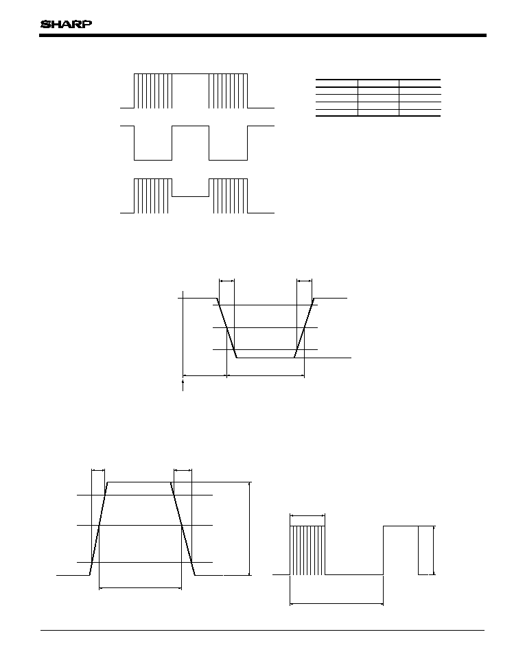
Signal Waveform
signal
16PSM code x1.5MHz
Receiver original output
Fig.3
Example of Signal Waveform
Mode
Mode1
Mode2
Mode3
Mode4
Txcnt1
0
0
1
1
0
1
0
1
1
1
1
1
1
1/2
1/4
1/8
Txcnt2
Txin
LED output power
4 range of LED power control. Refer to Fig.3
LEDA
TXD
RESET
SD
T
X
cnt1
V
O
AV
CC
V
CC
1
=
3.3V
V
CC
=
3.3V
V
CC
=
3.3V
IRT
X
FEPWR
1
T
X
cnt2
FEPWR
0
T
X
bias
IRT
X
bias
FERESET
FECNT
V
CC
SI
SCK
CMD
MSG
SO
RDY
CLK6M
GND
Control IC
6MHz CLCK
10pF
160k
Microcomputer
Fig.2
System Configuration
GP2W2003YK/GP2W2004YK
Fig.7
Output Waveform (Transmitter side)
t
f
t
ws
t
r
90%
50%
10%
t
j
V
OH
V
OL
Pulse
reference portion
Fig.6
Output Waveform (Receiver side)
t
f
Pulse width
t
r
90%
50%
10%
T
6.67
µ
s
I
E
100mW/sr
The light emitting diode
(SHARP GL710,
p
=
850 to 900nm)
is used as the transmitter,
where the following continuous signals are transmitted.
Fig.5
Txbias Output Waveform
TXD
T
X
bias
TXD
T
X
bias
DC bias
0
0
OFF
0
1
OFF
1
0
OFF
1
1
ON
V
O
T
X
bias truth table
DC bias voltage can be superimposed on V
O
output, applying signal waveform shown on
the left to T
Xbias
teminal. Refer to Fig.3