 | –≠–ª–µ–∫—Ç—Ä–æ–Ω–Ω—ã–π –∫–æ–º–ø–æ–Ω–µ–Ω—Ç: GPIS94 | –°–∫–∞—á–∞—Ç—å:  PDF PDF  ZIP ZIP |

(Ta=25∞C)
I
F
50
mA
V
R
6
V
P
75
mW
V
CEO
35
V
V
ECO
6
V
I
C
20
mA
P
C
75
mW
P
tot
T
opr
100
mW
∞C
T
stg
∞C
T
sol
260
∞C
Absolute Maximum Ratings
1. Subminiature wide-gap type
4. With positioning boss
1. FDDs
2. Laser disc players
Input
Output
Parameter
Symbol
Rating
Unit
- 25 to + 85
- 40 to + 100
Forward current
Reverse voltage
Power dissipation
Collector-emitter voltage
Emitter-collector voltage
Collector current
Collector power dissipation
Total power dissipation
Operating temperature
Storage temperature
Soldering temperature
*1
1 mm or more
Soldering area
(Unit : mm)
* Tolerance :
±
0.2
* Burrs dimensions : 0.15 MAX.
*( ) : Reference dimensions
The dimensions indicated by
g
refer
to those measured from the lead base.
3. Slit : (0.3) mm
GP1S94
GP1S94
2. Emitter-detector gap width : 3.5 mm
3. VCRs
Features
Applications
Outline Dimensions
*1 For MAX. 5 seconds
Subminiature Wide-gap Type
Photointerrupter
Top View
4 Cathode
3 Emitter
2 Collector
1 Anode
Circuit diagram
:
Top View
(0.3) Slit width
3.4
3.6
±
0.5
5.2
0.4
g
2.54
(C0.4)
4 Z
S
a-a section
3.5
(0.85)
6.0
3.5
g
5.0
0.15
(C0.3)
Optical
center
0.8
1.1
(C0.2)
+
0.2
-
0.1
1.1
+
0
-
0.1
0.9
+
0
-
0.1
4
1
2
3
aa
1.2
4
1
2
3
data books, etc. Contact SHARP in order to obtain the latest version of the device specification sheets before using any SHARP's device.
"
"
In the absence of confirmation by device specification sheets, SHARP takes no responsibility for any defects that occur in equipment using any of SHARP's devices, shown in catalogs,
s
s
s
s

V
F
I
F
= 20mA
-
1.2
1.4
V
I
R
V
R
= 3V
-
-
10
µ
A
I
CEO
V
CE
= 20V
-
-
100
nA
I
C
V
CE
= 5V, I
F
= 5mA
40
-
400
µ
A
V
CE(sat)
I
F
= 10mA, I
C
= 40
µ
A
-
-
0.4
V
V
CE
= 5V, I
C
= 100
µ
A
R
L
-
50
150
µ
s
-
50
150
µ
s
- 25
0
25
50
75
100
0
10
20
30
40
50
60
- 25
0
25
50
75
100
0
20
40
60
80
85
100
120
85
t
r
t
f
0
0.5
1
1.5
2
1
2
10
20
100
200
2.5
3
5
50
500
25∞C
0∞C
- 25∞C
50∞C
= 1 000
T
a
= 75∞C
(Ta=25∞C)
Electro-optical Characteristics
Fig. 1 Forward Current vs. Ambient
Temperature
Fig. 2 Power Dissipation vs. Ambient
Temperature
Fig. 4 Collector Current vs. Forward Current
Fig. 3 Forward Current vs. Forward Voltage
Parameter
Symbol
Conditions
MIN.
TYP.
MAX.
Unit
Input
Output
Transfer
characteristics
Forward voltage
Reverse current
Dark current
Collector current
Collector-emitter saturation voltage
Response time
Rise time
Fall time
Forward current I
F
(
mA
)
Ambient temperature Ta (∞C)
Power dissipation P (mW)
Ambient temperature Ta (∞C)
Collector current Ic (mA)
Forward current I
F
(mA)
Forward current I
F
(
mA
)
Forward voltage V
F
(V)
GP1S94
0
10
20
0
0.2
0.4
0.6
0.8
1.0
V
CE
=5V
Ta =25∞C
Total power dissipation
Input side power dissipation and
output side collector power dissipation
s

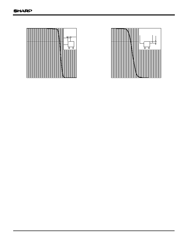
Fig. 5 Collector Current vs. Collector-emitter
Voltage
Fig. 7 Collector-emitter Saturation Voltage
vs. Ambient Temperature
Test Circuit for Response Time
Collector current Ic (mA)
Collector-emitter voltage V
CE
(V)
Ambient temperature Ta (∞C)
Relative collector current (%)
Collector-emitter saturation voltage V
CE
( sat
)
(
V
)
Ambient temperature Ta (∞C)
2
5
2
5
2
5
2
5
25
50
75
100
0
10
%
90
%
R
D
V
CC
R
L
t
d
t
r
t
s
t
f
V
CE
= 20V
10
- 10
10
- 9
10
- 8
10
- 7
10
- 6
Response time (
µ
s)
Load resistance R
L
(k
)
Ambient temperature Ta (∞C)
Fig. 8 Dark Current vs. Ambient Temperature
Input
Output
Input
Output
GP1S94
Dark current I
CEO
(
A
)
Fig. 9 Response Time vs. Load Resistance
Fig. 6 Relative Collector Current vs.
Ambient Temperature
0.1
1
5
10
50
100
1
5
10
50
100
500
1000
tr
tf
td
ts
V
CE
=5V
I
C
=100
µ
A
- 25
0
25
50
75 85
0.06
0.08
0.10
0.12
0.14
0.16
0.18
0.20
I
F
=10mA
I
C
=40
µ
A
- 25
0
25
50
75 85
120
110
100
90
80
70
60
50
40
30
20
10
0
I
F
=5mA
V
CE
=5V
0
4
2
8
6
10
5mA
10mA
I
F
=50mA
20mA
30mA
40mA
0
0.4
0.6
0.8
1.0
0.2
GP1S94
Relative collector current (%)
Relative collector current (%)
Shield distance L (mm)
Shield distance L (mm)
Please refer to the chapter "Precautions for Use".
Fig. 10 Detecting Position Characteristics (1)
Fig. 11 Detecting Position Characteristics (2)
0
0.5
1
1.5
2
2.5
0
10
20
30
40
50
60
70
80
90
100
L=0
L
I
F
=5mA
V
CE
=5V
0
0.5
1
1.5
2
0
10
20
30
40
50
60
70
80
90
100
L=0
L
I
F
=5mA
V
CE
=5V
q

115
Application Circuits
NOTICE
qThe circuit application examples in this publication are provided to explain representative applications of
SHARP devices and are not intended to guarantee any circuit design or license any intellectual property
rights. SHARP takes no responsibility for any problems related to any intellectual property right of a
third party resulting from the use of SHARP's devices.
qContact SHARP in order to obtain the latest device specification sheets before using any SHARP device.
SHARP reserves the right to make changes in the specifications, characteristics, data, materials,
structure, and other contents described herein at any time without notice in order to improve design or
reliability. Manufacturing locations are also subject to change without notice.
qObserve the following points when using any devices in this publication. SHARP takes no responsibility
for damage caused by improper use of the devices which does not meet the conditions and absolute
maximum ratings to be used specified in the relevant specification sheet nor meet the following
conditions:
(i) The devices in this publication are designed for use in general electronic equipment designs such as:
--- Personal computers
--- Office automation equipment
--- Telecommunication equipment [terminal]
--- Test and measurement equipment
--- Industrial control
--- Audio visual equipment
--- Consumer electronics
(ii)Measures such as fail-safe function and redundant design should be taken to ensure reliability and
safety when SHARP devices are used for or in connection with equipment that requires higher
reliability such as:
--- Transportation control and safety equipment (i.e., aircraft, trains, automobiles, etc.)
--- Traffic signals
--- Gas leakage sensor breakers
--- Alarm equipment
--- Various safety devices, etc.
(iii)SHARP devices shall not be used for or in connection with equipment that requires an extremely
high level of reliability and safety such as:
--- Space applications
--- Telecommunication equipment [trunk lines]
--- Nuclear power control equipment
--- Medical and other life support equipment (e.g., scuba).
qContact a SHARP representative in advance when intending to use SHARP devices for any "specific"
applications other than those recommended by SHARP or when it is unclear which category mentioned
above controls the intended use.
qIf the SHARP devices listed in this publication fall within the scope of strategic products described in the
Foreign Exchange and Foreign Trade Control Law of Japan, it is necessary to obtain approval to export
such SHARP devices.
qThis publication is the proprietary product of SHARP and is copyrighted, with all rights reserved. Under
the copyright laws, no part of this publication may be reproduced or transmitted in any form or by any
means, electronic or mechanical, for any purpose, in whole or in part, without the express written
permission of SHARP. Express written permission is also required before any use of this publication
may be made by a third party.
qContact and consult with a SHARP representative if there are any questions about the contents of this
publication.