 | –≠–ª–µ–∫—Ç—Ä–æ–Ω–Ω—ã–π –∫–æ–º–ø–æ–Ω–µ–Ω—Ç: LH155BA | –°–∫–∞—á–∞—Ç—å:  PDF PDF  ZIP ZIP |
Document Outline
- ˛ˇ
- ˛ˇ
- ˛ˇ
- ˛ˇ
- ˛ˇ
- ˛ˇ
- ˛ˇ
- ˛ˇ
- ˛ˇ
- ˛ˇ
- ˛ˇ
- ˛ˇ
- ˛ˇ
In the absence of confirmation by device specification sheets, SHARP takes no responsibility for any defects that may occur in equipment using any SHARP devices shown in
catalogs, data books, etc. Contact SHARP in order to obtain the latest device specification sheets before using any SHARP device.
1
DESCRIPTION
The LH155BA is an LCD driver with a built-in RAM
suitable for driving medium/small scale dot-matrix
LCD panels, and which is capable of being directly
connected to the bus line of a microcomputer. The
LH155BA stores in the RAM the 8-bit parallel or
serial display data transferred from the
microcomputer and generates LCD drive signals.
Since the LH155BA features a bit-map type LCD
driver that one bit of data in the display RAM
corresponds to one dot in the LCD, there is a lot of
freedom in displaying. The LH155BA has 128
segment outputs and 64 common outputs in a
single chip, making it possible to create an LCD
system with the fewest number of the chips. The
LH155BA enables an LCD system for battery-
operated, hand-carrying information equipment by
securing lower power consumption and wider
operating voltage range.
FEATURES
∑ Graphic display output pin : 64 x 128 pins
∑ Segment display output pin : 3 x 12 pins
∑ Icon display output pin : 1 x 1 pin
∑ LCD display by graphic display RAM
≠ Normal mode : RAM data "0"/not lighted,
RAM data "1"/lighted
≠ Reverse mode : RAM data "1"/not lighted,
RAM data "0"/lighted
∑ Display RAM memory capacity
≠ 128 x 64 = 8 192 bits (For graphic display)
≠ 12 x 3 = 36 bits (For segment display)
≠ 1 x 1 = 1 bit (For icon display)
∑ General 8-bit MPU interface : Possible to directly
connect 80-family and 68-family MPUs to bus line
∑ Possible to make serial interface
∑ Ratio of display duty cycle :
1/16, 1/32, 1/48 or 1/64 (selectable by command)
∑ 128-bit automatic transfer from display RAM to
display data latch
∑ Abundant command functions
≠ Display data read/write
≠ Setting up LCD alternating signal cycle
≠ Setting up display starting-line : per line
≠ Display ON/OFF
≠ Display control of normal and reverse modes
≠ Increment control of display RAM address
≠ Write control of read modifying
≠ Internal register read
≠ Power saving mode
∑ LCD drive power circuit
≠ Built-in booster circuit : Two, three or four times
voltage boost is possible
≠ Built-in voltage converter : Generates LCD
drive voltages (V
0
, V
1
, V
2
, V
3
and V
4
) based
on the boosted voltage
≠ Built-in power bias ratio : 1/7 or 1/9 bias
(selectable by command)
≠ Built-in electronic volume : Controllable in 16
steps
≠ Supply voltages
Logic system : +1.8 to +5.5 V
LCD drive system : +4.0 to +14.0 V
∑ Operating temperature : ≠30 to +85 ∞C
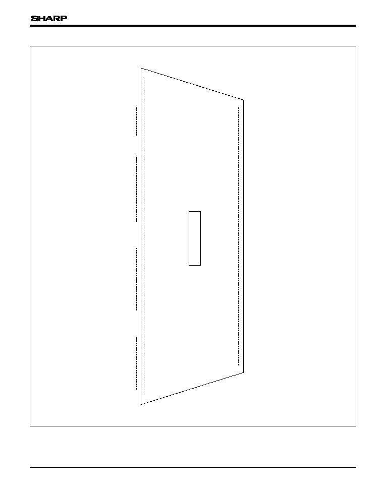
∑ Package : 260-pin TCP (Tape Carrier Package)
LH155BA
LH155BA
128-Segment and 64-Common Outputs
LCD Driver IC with A Built-in RAM
PIN CONNECTIONS
LH155BA
2
209
210
260
1
COMS
0
COMS
1
COMS
2
SEGS
0
SEGS
1
ICON
2
ICON
1
COM
31
COM
30
SEGS
11
SEGS
10
COM
63
COM
62
COM
33
COM
32
SEG
127
SEG
126
SEG
125
SEG
2
SEG
1
SEG
0
COM
0
COM
1
CHIP SURFACE
V
A
V
B
V
C
V
D
V
R2
V
R1
V
OUT
V
EE3
SVOUT
V
EE2
SVR
CAP+
CAP≠
V
EE
V
DD
PMODE
EXA
CKS
CK
V
SS
OSCI
OSCO
V
SS
M
FLM
LP
D
7
D
6
D
5
D
4
D
3
D
2
D
1
D
0
RDB
WRB
SCL
SDA
P/S
M86
M/S
RS
CSB
RESB
TEST
V
SS
V
4
V
3
V
2
V
1
V
0
260-PIN TCP
TOP VIEW
NOTE :
Doesn't prescribe TCP outline.
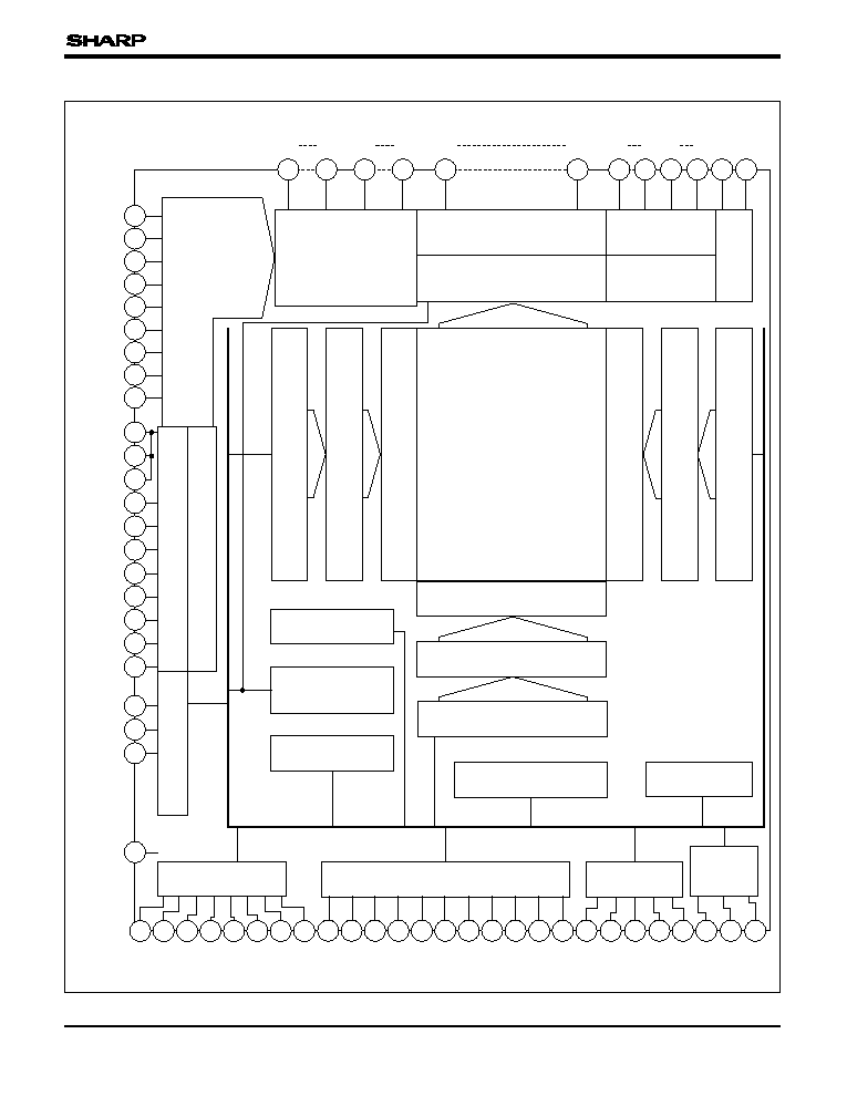
BLOCK DIAGRAM
LH155BA
3
50
49
242
CK
CKS
OSCO
240
OSCI
244
EXA
237
M
FLM
235
LP
218
CSB
219
RS
220
M/S
221
M86
226
RDB
225
WRB
217
RESB
222
P/S
223
SDA
224
SCL
216
TEST
234
D
7
233
D
6
232
D
5
231
D
4
230
D
3
229
D
2
228
D
1
227
D
0
215
V
SS
V
SS
V
SS
238
241
249
CAP+
248
CAP≠
251
V
EE2
253
V
EE3
247
V
EE
245
PMODE
252
SVOUT
254
V
OUT
255
V
R1
V
R2
250
SVR
246
V
DD
257
V
D
258
V
C
259
V
B
210
V
0
260
V
A
3
COMS
0
COMS
2
5
6
SEGS
0
17
SEGS
11
SEG
127
COM
0
SEG
0
COM
31
COM
32
209
1
COM
63
ICON
1
2
ICON
2
SEGMENT DRIVER
SEGMENT
COMMON
DRIVER
SHIFT
REGISTER
DATA LATCH
DC-DC CONVERTER
LCD POWER SUPPLY
ELECTRONIC VOLUME
Y ADDRESS REGISTER
Y ADDRESS COUNTER
ICON
I/O BUFFER
MPU INTERFACE
OSC
DISPLAY
TIMING
GENERATOR
213
V
3
212
V
2
211
V
1
214
V
4
18 178
243 239
236
177
X ADDRESS DECODER
X ADDRESS COUNTER
X ADDRESS REGISTER
Y ADDRESS DECODER
DISPLAY LINE COUNTER
LINE ADDRESS DECODER
DISPLAY LINE REGISTER
DISPLAY RAM
64 x 128 BITS
(FOR GRAPHIC)
3 x 12 BITS
(FOR SEGMENT)
AC CONVERSION
CONTROL
BUS HOLDER
I/O BUFFER
COMMAND DECODER
REGISTER READ
CONTROL
256
4
LH155BA
SYMBOL
1. PIN DESCRIPTION
1.1. Power Supply Pins
I/O
DESCRIPTION
V
DD
Power Supply Power supply pin for logic, connected to +1.8 to +5.5 V.
V
SS
Power Supply Ground pin, connected to 0 V.
V
0
V
1
V
2
V
3
V
4
V
A
V
B
V
C
V
D
Power Supply
V
0
-V
4
for
Graphic
Display
V
A
-V
D
for
Segment
Display
Bias power supply pins for LCD drive voltage.
∑ When using an external power supply, convert impedance by using resistance-
division of LCD drive power supply or operational amplifier before adding voltage to
the pins.
∑ When using the external power supply, maintain the following power supply
conditions.
V
SS
< V
4
< V
3
< V
2
< V
1
< V
0
, V
SS
V
D
< V
C
< V
B
< V
A
∑ When the power supply circuit is ON at master operation, LCD drive voltages of V
0
to V
4
are generated by the internal booster circuit and voltage converter. When
using segment display, input V
A
, V
B
, V
C
and V
D
level externally.
∑ When using the internal power supply, be sure to connect each capacitor between
V
0
to V
4
, V
A
to V
D
, and V
SS
.
1.2. LCD Power Supply Circuit Pins
SYMBOL
I/O
DESCRIPTION
CAP+
O
Connecting pin for the internal booster's capacitor + side.
The capacitor is connected between CAP≠ and CAP+.
CAP≠
O
Connecting pin for the internal booster's capacitor ≠ side.
The capacitor is connected between CAP+ and CAP≠.
V
R1
V
R2
I
Used as input pins for graphic display voltage converter.
Voltage must be input between the V
EE
and V
OUT
pins by voltage divided by resistors.
V
EE3
O
Connecting pin for the internal booster's capacitor + side.
The capacitor is connected between V
SS
and V
EE3
.
V
EE2
O
Connecting pin for the internal booster's capacitor + side.
The capacitor is connected between V
SS
and V
EE2
.
Voltage supply pin for generating boosted voltage in the internal booster circuit.
Usually the same voltage level as V
DD
.
Power supply
V
EE
V
OUT
Power supply/
O
Output pin of boosted voltage in the internal booster circuit.
The capacitor must be connected between V
SS
and V
OUT
.
Non-connected.
≠
SVOUT
Non-connected.
≠
SVR
PMODE
Pin for controlling LCD power supply.
A combination of PMODE pin and ON/OFF command of power supply (PON)
enables selection of a specific drive operation.
I
5
LH155BA
1.3. System Bus Pins
SYMBOL
I/O
DESCRIPTION
CSB
I
Chip selection input pin that decoded address bus signal is input.
RS
I
Distinguishes display RAM data/commands of D
7
to D
0
data transferred from MPU.
0 : The data of D
7
to D
0
show the display RAM data.
1 : The data of D
7
to D
0
show the command data.
RDB
(E)
I
∑ In connecting to 80-family MPU :
This RDB is a pin for connecting the RDB signal of 80-family MPU. When the
signal enters in the "L" state, the data bus of this IC turns to the "output" state.
∑ In connecting to 68-family MPU :
This RDB becomes a pin for connecting the enable clock signal of 68-family MPU.
When the signal enters in the "H" state, the data bus of this IC turns to the "active"
state.
WRB
(R/W)
I
∑ In connecting to 80-family MPU :
This WRB is a pin for connecting the WRB signal of 80-family MPU, and when
WRB signal is "L", this pin is "active".
The data bus signal is input at the rising edge of WRB signal.
∑ In connecting to 68-family MPU :
This WRB becomes a pin for connecting the R/W signal of controlling read/write of
68-family MPU.
R/W = "H" : Read
R/W = "L" : Write
I
M86
MPU interface-type shift pin.
M86 = "H" : 68-family interface
M86 = "L" : 80-family interface
Fixed to either "H" or "L".
SDA
I
Serial-data input pin at time of serial interface selection.
SCL
I
Serial clock pin at time of serial interface selection.
Used to shift the SDA data by using the rising edge of SCL.
Used to convert into 8-bit data by using the 8th clock at the rising edge of SCL in
serial-to-parallel data processing.
After data-transferring, or when making no access, be sure to set to "L".
8-bit bi-directional data bus, connected to 8-bit MPU data bus.
I/O
D
7
-D
0
Initialized by setting to "L". The reset signals of the system are normally input. Reset
operation is performed in accordance with RESB signal level.
I
RESB
Used to shift between parallel interface and serial interface.
P/S = "H" for parallel input. Fix SDA and SCL pins to either "H" or "L".
P/S = "L" for serial input. Fix D
7
to D
0
pins to High-Z, RDB and WRB pins to either
"H" or "L".
I
P/S
TEST
I
For testing. Fix to "L".
P/S Chip selection Data identification
Data
Read/Write Serial clock
H
CSB
RS
D
7
-D
0
RDB, WRB
≠
L
CSB
RS
SDA
Write only
SCL