In the absence of confirmation by device specification sheets, SHARP takes no responsibility for any defects that may occur in equipment using any SHARP devices shown in
catalogs, data books, etc. Contact SHARP in order to obtain the latest device specification sheets before using any SHARP device.
1
LH1562
DESCRIPTION
The LH1562 is a 240-output segment/common
driver IC suitable for driving large/medium scale dot
matrix LCD panels, and is used in personal
computers/work stations. Through the use of SST
(Super Slim TCP) technology, it is ideal for
substantially decreasing the size of the frame
section of the LCD module. The LH1562 is good
both as a segment driver and a common driver,
and it can create a low power consuming, high-
resolution LCD.
FEATURES
∑ Number of LCD drive outputs : 240
∑ Supply voltage for LCD drive : +15.0 to +42.0 V
∑ Supply voltage for the logic system : +2.5 to +5.5 V
∑ Low power consumption
∑ Low output impedance
∑ Package : 269-pin TCP (Tape Carrier Package)
(Segment mode)
∑ Shift clock frequency
≠ 20 MHz (MAX.) : V
DD
= +5.0±0.5 V
≠ 15 MHz (MAX.) : V
DD
= +3.0 to +4.5 V
≠ 12 MHz (MAX.) : V
DD
= +2.5 to +3.0 V
∑ Adopts a data bus system
∑ 4-bit/8-bit parallel input modes are selectable with
a mode (MD) pin
∑ Automatic transfer function of an enable signal
∑ Automatic counting function which, in the chip
selection mode, causes the internal clock to be
stopped by automatically counting 240 bits of
input data
∑ Line latch circuits are reset when
active
(Common mode)
∑ Shift clock frequency : 4 MHz (MAX.)
∑ Built-in 240-bit bi-directional shift register
(divisible into 120 bits x 2)
∑ Available in a single mode (240-bit shift register)
or in a dual mode (120-bit shift register x 2)
q Y
1
/Y
240
Single mode
w Y
240
/Y
1
Single mode
e Y
1
/Y
120
, Y
121
/Y
240
Dual mode
r Y
240
/Y
121
, Y
120
/Y
1
Dual mode
The above 4 shift directions are pin-selectable
∑ Shift register circuits are reset when
active
PIN CONNECTIONS
LH1562
240-output LCD Segment/Common
Driver IC
240
241
269
1
Y
239
Y
240
Y
238
Y
3
Y
2
Y
1
CHIP SURFACE
V
0R
V
12R
V
43R
V
5R
V
SS
TEST
2
TEST
1
MD
L/R
FR
EIO
1
LP
DISPOFF
XCK
DI
7
DI
6
DI
5
DI
4
DI
3
DI
2
DI
1
DI
0
EIO
2
S/C
V
DD
V
5L
V
43L
V
12L
V
0L
269-PIN TCP
TOP VIEW
NOTE :
Doesn't prescribe TCP outline.
Back
LH1562
3
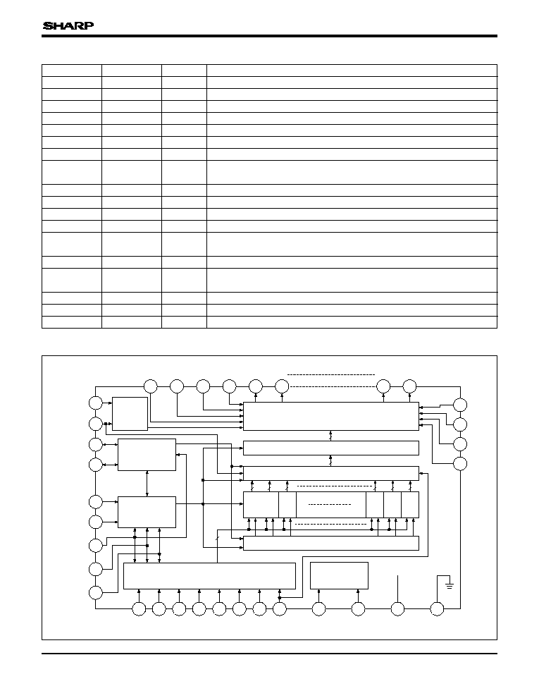
FUNCTIONAL OPERATIONS OF EACH BLOCK
4-Level Driver
Drives the LCD drive output pins from the line latch/shift register data, and selects one of
4 levels (V
0
, V
12
, V
43
, or V
5
) based on the S/C, FR and
signals.
The circuit for testing. During normal operation, it isn't activated.
Test Circuit
Controls the operation of each block. In case of segment mode, when an LP signal has
been input, all blocks are reset and the control logic waits for the selection signal output
from the active control block. Once the selection signal has been output, operation of the
data latch and data transmission is controlled, 240 bits of data are read in, and the chip
is non-selected. In case of common mode, controls the direction of data shift.
Control Logic
BLOCK
FUNCTION
Active Control
In case of segment mode, controls the selection or non-selection of the chip.
Following an LP signal input, and after the chip selection signal is input, a selection
signal is generated internally until 240 bits of data have been read in.
Once data input has been completed, a selection signal for cascade connection is
output, and the chip is non-selected.
In case of common mode, controls the input/output data of bi-directional pins.
The logic voltage signal is level-shifted to the LCD drive voltage level, and is output to
the driver block.
Level Shifter
In case of segment mode, selects the state of the data latch which reads in the data bus
signals. The shift direction is controlled by the control logic. For every 16 bits of data
read in, the selection signal shifts one bit based on the state of the control circuit.
Data Latch Control
In case of segment mode, keeps input data which are 2 clocks of XCK at 4-bit parallel
input mode in latch circuit, or keeps input data which are 1 clock of XCK at 8-bit parallel
input mode in latch circuit; after that they are put on the internal data bus 8 bits at a time.
SP Conversion
& Data Control
Data Latch
In case of segment mode, latches the data on the data bus. The latch state of each LCD
drive output pin is controlled by the control logic and the data latch control; 240 bits of
data are read in 30 sets of 8 bits.
In case of segment mode, all 240 bits which have been read into the data latch are
simultaneously latched at the falling edge of the LP signal, and are output to the level
shifter block. In case of common mode, shifts data from the data input pin at the falling
edge of the LP signal.
Line Latch/
Shift Register