In the absence of confirmation by device specification sheets, SHARP takes no responsibility for any defects that may occur in equipment using any SHARP devices shown in
catalogs, data books, etc. Contact SHARP in order to obtain the latest device specification sheets before using any SHARP device.
1
DESCRIPTION
The LH1687 is a 240-output TFT-LCD source
driver IC used in such products as TV sets. The
LH1687 samples and holds three video signals of
R, G and B by sample and hold circuits
synchronized with the CK, and simultaneously
outputs the LCD drive voltage from all output pins.
FEATURES
∑ Number of LCD drive outputs : 240
∑ Output circuit form : Push pull output
∑ Power save function : By setting the LCD drive
output in a high-impedance condition, the current
source of the LCD drive output circuit is cut off,
which makes low power operation possible
∑ Sampling timing : Normal sampling operation and
3-point simultaneous sampling operation can be
selected
∑ Video signal setting : Available for stripe pixel
array panels and delta pixel array panels using
mode setting circuit
∑ Sampling clock frequency : 25 MHz (MAX.)
∑ Cascade connection
∑ Sampling sequence :
Output shift direction can be selected
OS
1
/OS
240
or OS
240
/OS
1
∑ Output amplitude voltage :
4.8 Vp-p (at 5.0 V supply voltage)
∑ Supply voltages
≠ V
CC
L (for logic system) : +3.0 to +5.5 V
≠ V
CC
A (for LCD drive system) : +3.0 to +5.5 V
∑ Operating temperature : ≠30 to + 85 įC
∑ Package : 264-pin TCP (Tape Carrier Package)
PIN CONNECTIONS
LH1687
LH1687
240-output TFT-LCD Source Driver IC
OS
240
240
OS
1
1
CHIP SURFACE
V
CC
A
V
CC
L
GNDA
GNDL
TST
5
V
C
V
B
V
A
MODE
PS
RL
SAM
CTR
CK
SPIO
SPOI
TEST
4
TEST
3
TEST
2
TEST
1
GNDL
GNDA
V
CC
L
V
CC
A
264
263
262
261
260
259
258
257
256
255
254
253
252
251
250
249
248
247
246
245
244
243
242
241
264-PIN TCP
TOP VIEW
NOTE :
Doesn't prescribe TCP outline.
LH1687
2
PIN NO.
SYMBOL
I/O
DESCRIPTION
1 to 240
OS
1
-OS
240
O
LCD drive output pins
241, 264
V
CC
A
≠
Power supply pins for LCD drive circuit
242, 263
V
CC
L
≠
Power supply pins for logic circuit
243, 262
GNDA
≠
Ground pins for LCD drive system
244, 261
GNDL
≠
Ground pins for logic system
245 to 248
TST
1
-TST
4
I
IC test pins
249
SPOI
I/O
Start pulse input/cascade output pin
250
SPIO
I/O
Start pulse input/cascade output pin
251
CK
I
Horizontal shift clock input pin
252
CTR
I
LCD drive circuit operation selection pin
253
SAM
I
Sampling mode selection pin
254
RL
I
Sampling sequence selection pin
255
PS
I
Power save mode setting pin
256
MODE
I
Video signals form setting pin
257 to 259
V
A
, V
B
, V
C
I
Video signal input pins
IC test pin
I
TST
5
260
PIN DESCRIPTION
LH1687
4
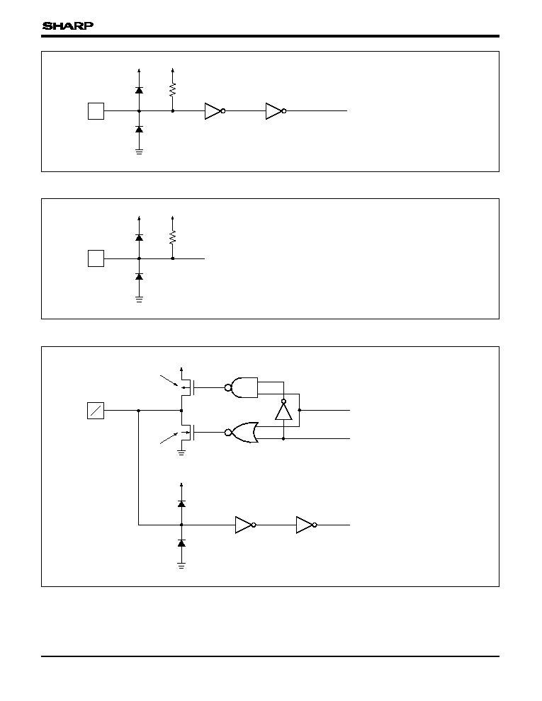
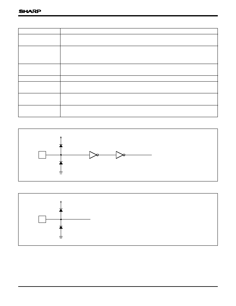
INPUT/OUTPUT CIRCUITS
I
V
CC
L
GNDL
To Internal Circuit
Fig. 1 Input Circuit (1)
ŅApplicable pins°
CK, CTR, MODE
I
V
CC
A
GNDA
To Internal Circuit
Fig. 2 Input Circuit (2)
ŅApplicable pins°
V
A
, V
B
, V
C
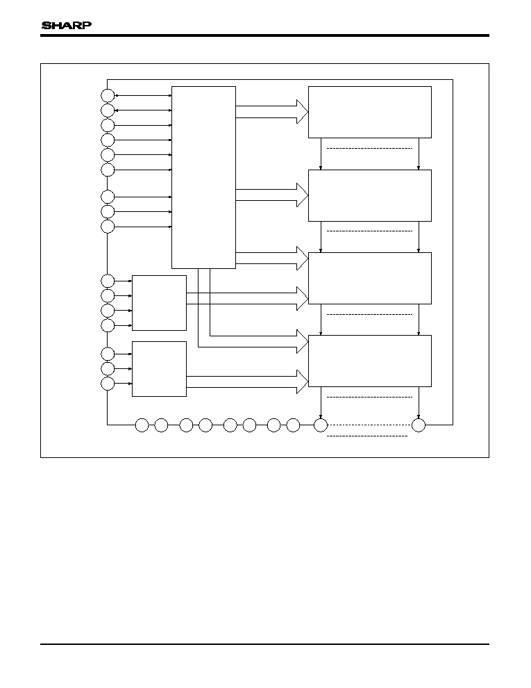
BLOCK
FUNCTION
Control Logic
Used to create signals necessary for each operation mode setting and sampling signal
creation circuits, etc.
Bi-directional Shift
Register
Used as transfer circuit of video sampling start signals.
It is possible to set the direction of sampling start signal sequence OS
1
/OS
240
or
OS
240
/OS
1
by setting the R/L pin.
Sampling Signal
Creation Circuit
Used to create the sampling signals corresponding to each output pin based on the
sampling start signals transferred by the bi-directional shift register.
Mode Setting Circuit
Used to set the form of the video signals to be sent to the sample and hold circuits.
Sample and Hold
Circuit
Used to sample the video signals input from the mode setting circuit at the timing of the
sampling signals and hold the sampling data until the next sampling operation.
Bias Generation Circuit Used to generate bias voltage necessary for output circuits.
Output Circuit
The circuit consists of a push-pull output operational amplifier and outputs the voltage
corresponding to the data held in the sample and hold circuits.
FUNCTIONAL OPERATIONS OF EACH BLOCK